F6N90 Datasheet. Specs and Replacement
Type Designator: F6N90 📄📄
Type of Transistor: MOSFET
Type of Control Channel: N-Channel
Absolute Maximum Ratings
Pd ⓘ - Maximum Power Dissipation: 33 W
|Vds|ⓘ - Maximum Drain-Source Voltage: 900 V
|Vgs|ⓘ - Maximum Gate-Source Voltage: 30 V
|Id| ⓘ - Maximum Drain Current: 6 A
Tj ⓘ - Maximum Junction Temperature: 150 °C
Electrical Characteristics
tr ⓘ - Rise Time: 17.2 nS
Cossⓘ - Output Capacitance: 100 pF
RDSonⓘ - Maximum Drain-Source On-State Resistance: 2.3 Ohm
Package: TO220F
📄📄 Copy
- MOSFET ⓘ Cross-Reference Search
F6N90 datasheet
..1. Size:1389K cn wxdh
f6n90.pdf 
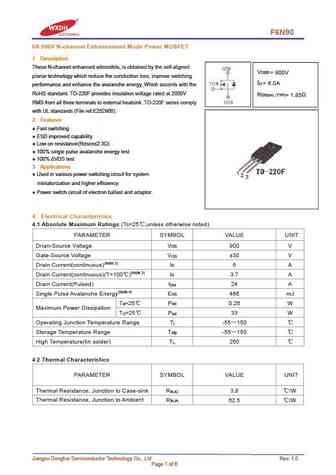
F6N90 6A 900V N-channel Enhancement Mode Power MOSFET 1 Description These N-channel enhanced vdmosfets, is obtained by the self-aligned V DSS = 900V planar technology which reduce the conduction loss, improve switching I = 6.0A D performance and enhance the avalanche energy. Which accords with the RoHS standard. TO-220F provides insulation voltage rated at 2000V R DS(on) TYP) = 1... See More ⇒
0.2. Size:710K 1
stf6n90k5.pdf
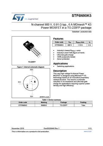
STF6N90K5 N-channel 900 V, 0.91 typ., 6 A MDmesh K5 Power MOSFET in a TO-220FP package Datasheet - production data Features Order code V R max. I DS DS(on) D STF6N90K5 900 V 1.10 6 A Industry s lowest R x area DS(on) Industry s best FoM (figure of merit) Ultra-low gate charge 100% avalanche tested Zener-protected TO-220FP Applications ... See More ⇒
0.3. Size:858K fairchild semi
fqpf6n90ct.pdf

TM QFET FQP6N90C/FQPF6N90C 900V N-Channel MOSFET General Description Features These N-Channel enhancement mode power field effect 6A, 900V, RDS(on) = 2.3 @VGS = 10 V transistors are produced using Fairchild s proprietary, Low gate charge ( typical 30 nC) planar stripe, DMOS technology. Low Crss ( typical 11 pF) This advanced technology has been especially tailored to ... See More ⇒
0.4. Size:860K fairchild semi
fqp6n90c fqpf6n90c.pdf
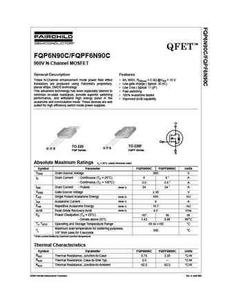
TM QFET FQP6N90C/FQPF6N90C 900V N-Channel MOSFET General Description Features These N-Channel enhancement mode power field effect 6A, 900V, RDS(on) = 2.3 @VGS = 10 V transistors are produced using Fairchild s proprietary, Low gate charge ( typical 30 nC) planar stripe, DMOS technology. Low Crss ( typical 11 pF) This advanced technology has been especially tailored to ... See More ⇒
0.5. Size:600K fairchild semi
fqpf6n90.pdf
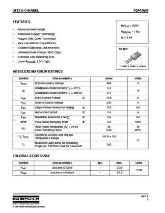
QFET N-CHANNEL FQPF6N90 FEATURES BVDSS = 900V Advanced New Design RDS(ON) = 1.9 Avalanche Rugged Technology ID = 3.4A Rugged Gate Oxide Technology Very Low Intrinsic Capacitances Excellent Switching Characteristics TO-220F Unrivalled Gate Charge 40nC (Typ.) Extended Safe Operating Area Lower RDS(ON) 1.5 (Typ.) 1 2 3 1. Gate 2. Drain 3. Sou... See More ⇒
0.6. Size:723K fairchild semi
fqaf6n90.pdf
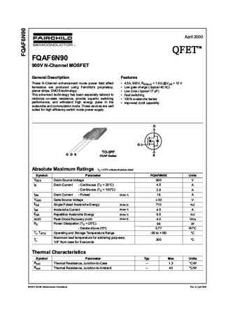
April 2000 TM QFET QFET QFET QFET 900V N-ChanneI MOSFET GeneraI Description Features These N-Channel enhancement mode power field effect 4.5A, 900V, RDS(on) = 1.9 @VGS = 10 V transistors are produced using Fairchild s proprietary, Low gate charge ( typical 40 nC) planar stripe, DMOS technology. Low Crss ( typical 17 pF) This advanced technology has been es... See More ⇒
0.7. Size:1255K onsemi
fqp6n90c fqpf6n90c.pdf

Is Now Part of To learn more about ON Semiconductor, please visit our website at www.onsemi.com Please note As part of the Fairchild Semiconductor integration, some of the Fairchild orderable part numbers will need to change in order to meet ON Semiconductor s system requirements. Since the ON Semiconductor product management systems do not have the ability to manage part nomenclatur... See More ⇒
0.8. Size:184K aosemi
aotf6n90.pdf
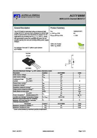
AOTF6N90 900V,6A N-Channel MOSFET General Description Product Summary VDS 1000V@150 The AOTF6N90 is fabricated using an advanced high voltage MOSFET process that is designed to deliver high ID (at VGS=10V) 6A levels of performance and robustness in popular AC-DC RDS(ON) (at VGS=10V) ... See More ⇒
0.10. Size:1096K bruckewell
msf6n90.pdf

MSF6N90 900V N-Channel MOSFET Description The MS15N50 is a N-channel enhancement-mode MOSFET, providing the designer with the best combination of fast switching, ruggedized device design, low on-resistance and cost effectiveness. The ITO-220 package is universally preferred for all commercial-industrial applications Features RDS(on) (Max 2.4 )@VGS=10V Gate Charg... See More ⇒
0.11. Size:1057K feihonltd
fhp6n90a fhf6n90a.pdf
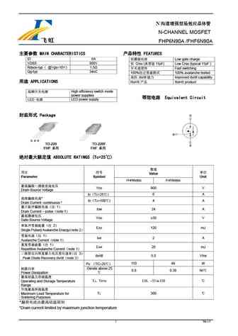
N N-CHANNEL MOSFET FHP6N90A /FHF6N90A MAIN CHARACTERISTICS FEATURES ID 6A Low gate charge VDSS 900V Crss ( 11pF) Low Crss (typical 11pF ) Rdson-typ @Vgs=10V 1.5 Fast switching Qg-typ 34nC 100% 100% avalanche tested dv/dt Improv... See More ⇒
0.12. Size:752K samwin
swf6n90d swj6n90d.pdf
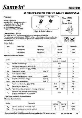
SW6N90D N-channel Enhanced mode TO-220F/TO-262N MOSFET TO-220F TO-262N Features BVDSS 900V ID 6A High ruggedness Low RDS(ON) (Typ 1.8 )@VGS=10V RDS(ON) 1.8 Low Gate Charge (Typ 42nC) Improved dv/dt Capability 2 1 1 100% Avalanche Tested 2 2 3 3 Application UPS, LED, SMPS 1 1. Gate 2. Drain 3. Source 3 General Description ... See More ⇒
0.13. Size:252K inchange semiconductor
aotf6n90.pdf
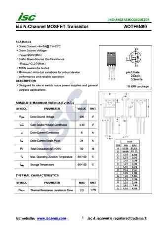
isc N-Channel MOSFET Transistor AOTF6N90 FEATURES Drain Current I =6A@ T =25 D C Drain Source Voltage- V =900V(Min) DSS Static Drain-Source On-Resistance R =2.2 (Max) DS(on) 100% avalanche tested Minimum Lot-to-Lot variations for robust device performance and reliable operation DESCRIPTION Designed for use in switch mode power supplies and general purpose a... See More ⇒
0.14. Size:279K inchange semiconductor
stf6n90k5.pdf
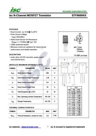
isc N-Channel MOSFET Transistor STF6N90K5 FEATURES Drain Current I = 6.0A@ T =25 D C Drain Source Voltage V = 900V(Min) DSS Static Drain-Source On-Resistance R = 1.1 (Max) @ V = 10V DS(on) GS 100% avalanche tested Minimum Lot-to-Lot variations for robust device performance and reliable operation DESCRIPTION motor drive, DC-DC converter, power switch and sole... See More ⇒
Detailed specifications: F4N65, F4N70, F50N06, F50N20, F5N65C, F5N80, F630, F640, IRF630, F740, F7N60, F7N70, F7N80, F80N06, F8N50, F8N60, F8N65
Keywords - F6N90 MOSFET specs
F6N90 cross reference
F6N90 equivalent finder
F6N90 pdf lookup
F6N90 substitution
F6N90 replacement
Can't find your MOSFET?
Learn how to find a substitute transistor by analyzing voltage, current and package compatibility