JVC105E Specs and Replacement
Type Designator: JVC105E
Type of Transistor: MOSFET
Type of Control Channel: N-Channel
Absolute Maximum Ratings
Pd ⓘ - Maximum Power Dissipation: 178 W
|Vds|ⓘ - Maximum Drain-Source Voltage: 100 V
|Vgs|ⓘ - Maximum Gate-Source Voltage: 20 V
|Id| ⓘ - Maximum Drain Current: 135 A
Tj ⓘ - Maximum Junction Temperature: 150 °C
Electrical Characteristics
tr ⓘ - Rise Time: 23 nS
Cossⓘ - Output Capacitance: 592 pF
RDSonⓘ - Maximum Drain-Source On-State Resistance: 0.0053 Ohm
Package: TO220
JVC105E substitution
- MOSFET ⓘ Cross-Reference Search
JVC105E datasheet
jvc105e.pdf
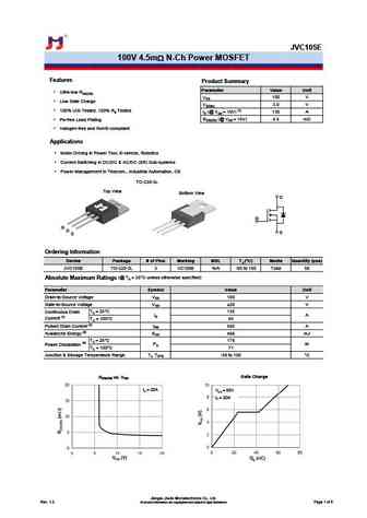
JVC105E 100V 4.5mW N-Ch Power MOSFET Features Product Summary Parameter Value Unit Ultra-low RDS(ON) VDS 100 V Low Gate Charge VGS(th) 3.0 V 100% UIS Tested, 100% Rg Tested ID (@ VGS = 10V) (1) 135 A RDS(ON) (@ VGS = 10V) 4.5 mW Pb-free Lead Plating Halogen-free and RoHS-compliant Applications Motor Driving in Power Tool, E-vehicle, Robotics Curr... See More ⇒
jvc103k.pdf
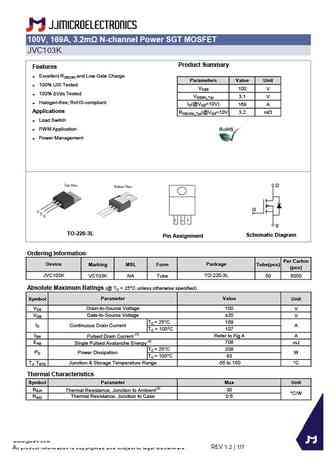
100V, 169A, 3.2m N-channel Power SGT MOSFET JVC103K Product Summary Features Excellent RDS(ON) and Low Gate Charge Parameters Value Unit 100% UIS Tested VDSS 100 V 100% Vds Tested VGS(th)_Typ 3.1 V Halogen-free; RoHS-compliant ID(@VGS=10V) 169 A Applications RDS(ON)_Typ(@VGS=10V 3.2 mW Load Switch PWM Application Power Management D G S TO-22... See More ⇒
jvc103t.pdf
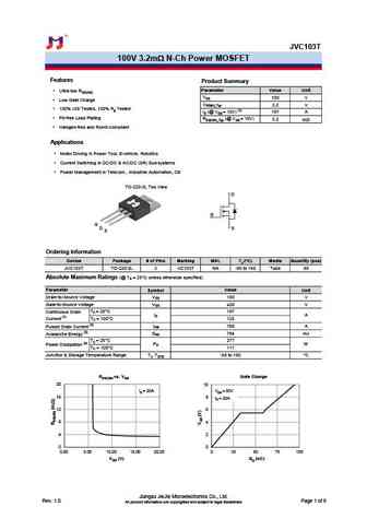
JVC103T 100V 3.2mW N-Ch Power MOSFET Features Product Summary Parameter Value Unit Ultra-low RDS(ON) Ultra-low RDS(ON) VDS 100 V Low Gate Charge Low Gate Charge VGS(th)_Typ 3.2 V 100% UIS Tested, 100% Rg Tested 100% UIS Tested, 100% RgTested ID (@ VGS = 10V) (1) 197 A Pb-free Lead Plating RDS(ON)_Typ (@ VGS = 10V) Pb-free Lead Plating 3.2 mW... See More ⇒
Detailed specifications: JVL102T, JVL102Y, JMTV3400A, JMTY11DN10A, JMTY2310A, JVC085T, JVC103K, JVC103T, 2N60, JVC113T, JVC502E, SLA08N10G, SLA10N03T, SLB60R105E7D, SLB65R380E7C, SLC013RN06G, SLD07RN10G
Keywords - JVC105E MOSFET specs
JVC105E cross reference
JVC105E equivalent finder
JVC105E pdf lookup
JVC105E substitution
JVC105E replacement
Can't find your MOSFET? Learn how to find a substitute transistor by analyzing voltage, current and package compatibility
History: BUK445-60H | 2SK3036 | 2SJ360 | KHB8D8N25F | SRC60R075BS
🌐 : EN ES РУ

LIST
Last Update
MOSFET: AUB034N10 | AUB033N08BG | AUB026N085 | AUA062N08BG | AUA060N08AG | AUA056N08BGL | AUA039N10 | ASW80R290E | ASW65R120EFD | ASW65R110E
Popular searches
kta1381 | bf494 | 2sc1885 | skd502t | 2sb754 | 2sc2362 | 2sd468 | c2240 transistor