AGM302D1 Datasheet. Specs and Replacement
Type Designator: AGM302D1 📄📄
Type of Transistor: MOSFET
Type of Control Channel: N-Channel
Absolute Maximum Ratings
Pd ⓘ - Maximum Power Dissipation: 83 W
|Vds|ⓘ - Maximum Drain-Source Voltage: 30 V
|Vgs|ⓘ - Maximum Gate-Source Voltage: 20 V
|Id| ⓘ - Maximum Drain Current: 180 A
Tj ⓘ - Maximum Junction Temperature: 150 °C
Electrical Characteristics
tr ⓘ - Rise Time: 45 nS
Cossⓘ - Output Capacitance: 520 pF
RDSonⓘ - Maximum Drain-Source On-State Resistance: 0.0028 Ohm
Package: TO252
📄📄 Copy
AGM302D1 substitution
- MOSFET ⓘ Cross-Reference Search
AGM302D1 datasheet
agm302d1.pdf
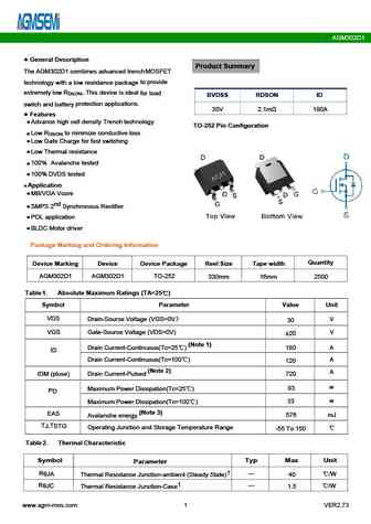
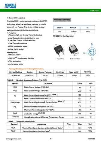
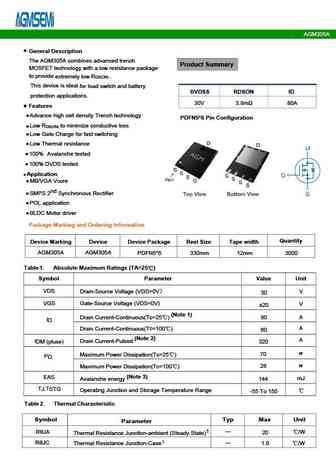
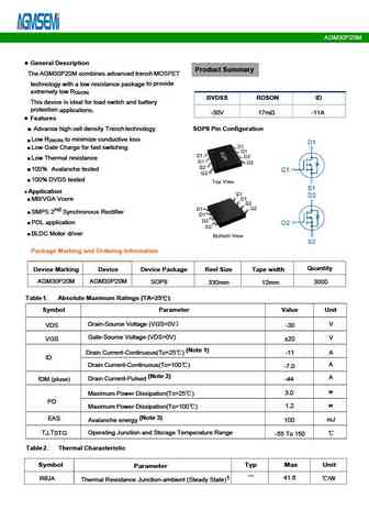
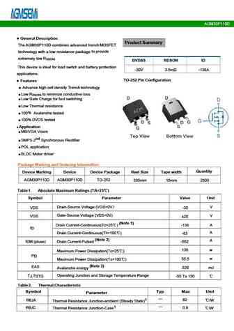
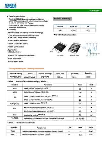
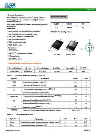
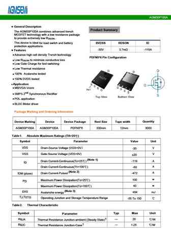
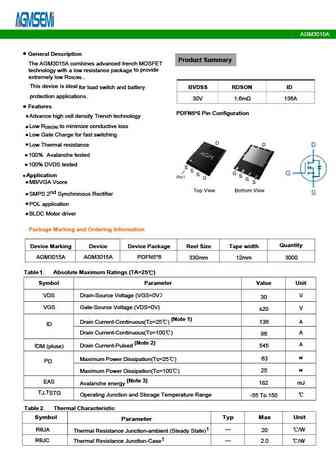
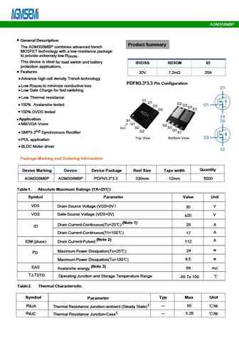
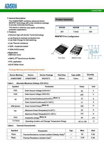
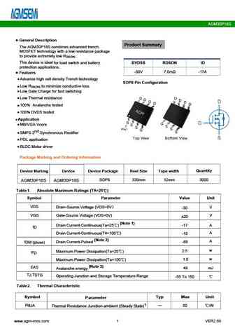
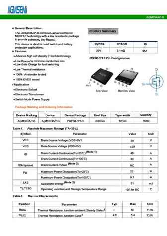
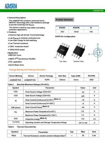
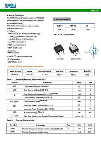
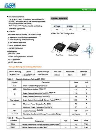
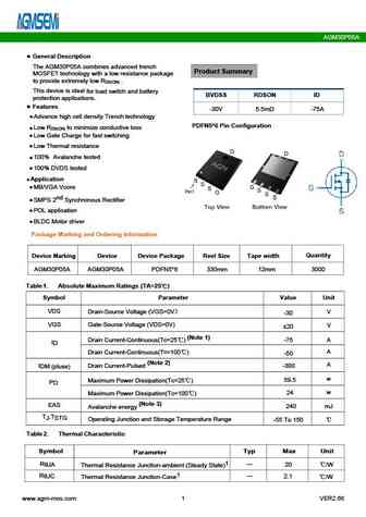
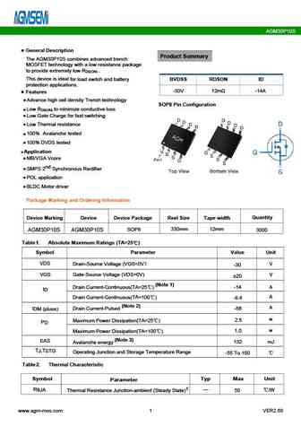
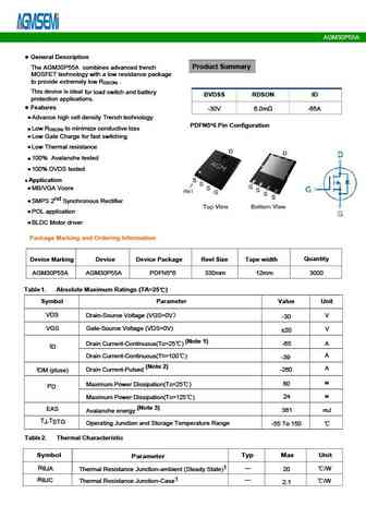
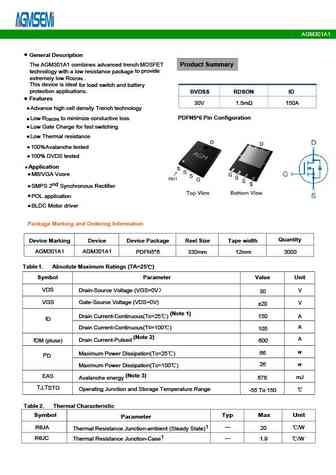
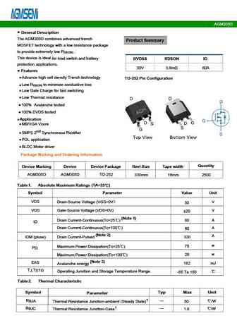
AGM302D1 General Description Product Summary The AGM302D1 combines advanced trenchMOSFET to provide technology with a low resistance package extremely low R .This device is ideal DS(ON) for load BVDSS RDSON ID protection applications. switch and battery 30V 2.1m 180A Features Advance high cell density Trench technology TO-252 Pin Configuration Low R to minimize... See More ⇒
agm302c1.pdf
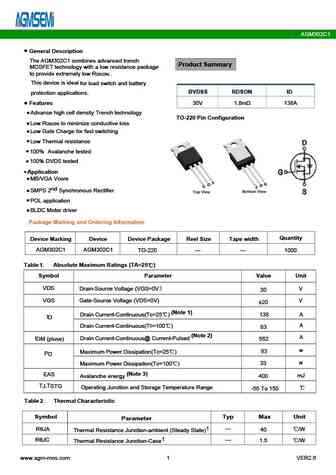
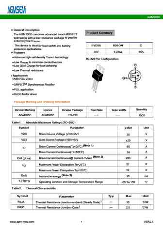
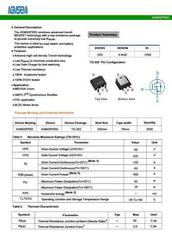
AGM302C1 General Description The AGM302C1 combines advanced trench Product Summary MOSFET technology with a low resistance package to provide extremely low R . DS(ON) This device is ideal for load switch and battery BVDSS RDSON ID protection applications. Features 30V 1.8m 138A Advance high cell density Trench technology TO-220 Pin Configuration Low R to minimi... See More ⇒
agm302a1.pdf
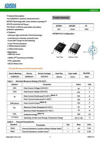
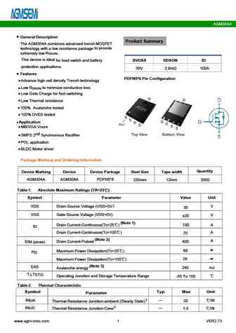
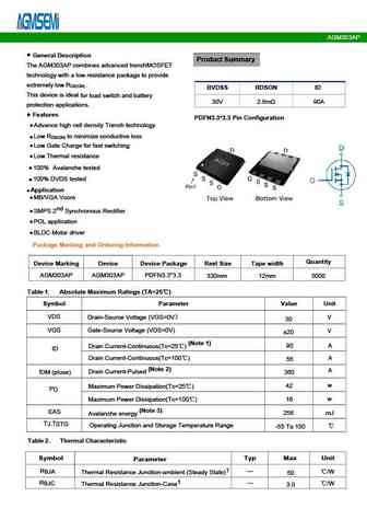
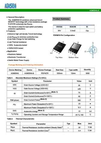
AGM302A1 General Description Product Summary The AGM302A1 combines advanced trench to MOSFETtechnology with a low resistance package provide extremely low R . DS(ON) BVDSS RDSON ID This device is ideal for load switch and battery 30V 1.8m 180A protection applications. Features PDFN5*6 Pin Configuration Advance high cell density Trench technology Low R to min... See More ⇒
agm308ma.pdf
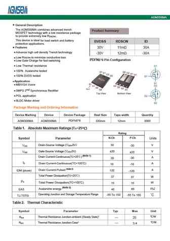
AGM308MA Table 3. N- Channel Electrical Characteristics (TJ=25 unless otherwisenoted) Symbol Parameter Conditions Min Typ Max Unit On/Off States BV Drain-Source Breakdown Voltage V =0V I =250 A 30 -- -- V GS D DSS Zero Gate Voltage Drain Current V =30V,V =0V -- -- 1 A DS GS I DSS Gate-Body Leakage Current V = 20V,V =0V -- -- nA GS DS 100 I GSS VGS(th) Gate Threshold Vo... See More ⇒
agm303d1.pdf
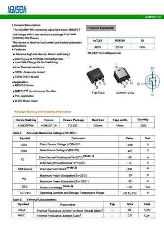
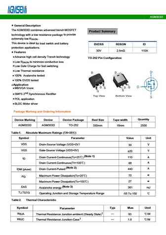
AGM303D1 General Description Product Summary The AGM303D1 combines advanced trenchMOSFET to provide technology with a low resistance package extremely low R .This device is ideal DS(ON) for load BVDSS RDSON ID protection applications. switch and battery 30V 2.0m 100A Features Advance high cell density Trench technology TO-252 Pin Configuration Low R to minimize... See More ⇒
agm305ap.pdf
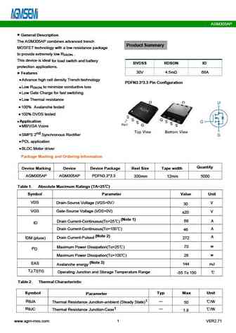
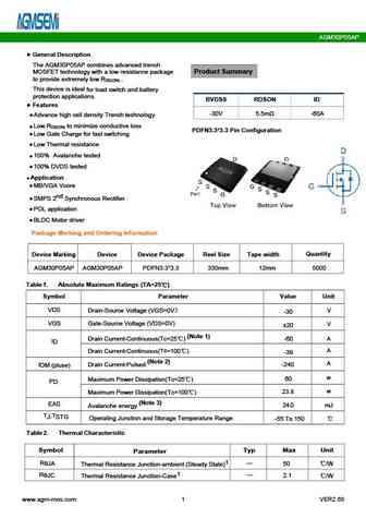
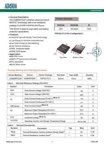
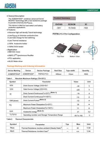
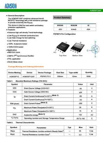
AGM305AP General Description The AGM305AP combines advanced trench Product Summary MOSFET technology with a low resistance package to provide extremely low R . DS(ON) This device is ideal for load switch and battery BVDSS RDSON ID protection applications. 30V 4.5m 68A Features Advance high cell density Trench technology PDFN3.3*3.3 Pin Configuration Low R to ... See More ⇒
agm30p25mbp.pdf
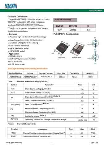
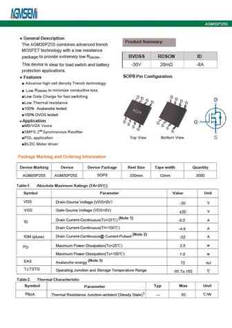
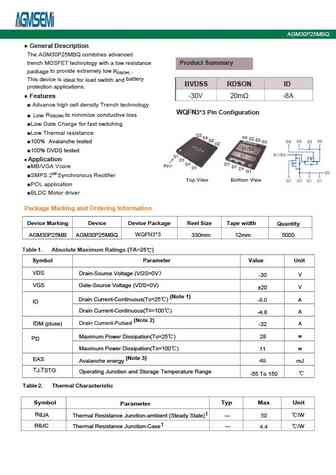
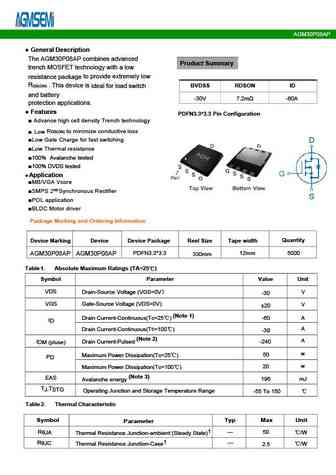
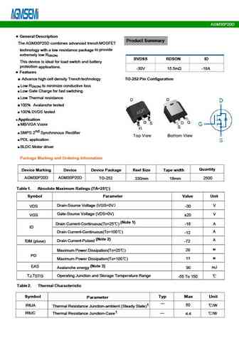
AGM30P25MBP General Description The AGM30P25MBP combines advanced trench Product Summary MOSFET technology with a low resistance to provide extremely low R . package DS(ON) BVDSS RDSON ID This device is ideal for load switch and battery -30V 20m -8A protection applications. Features PDFN3*3 Pin Configuration Advance high cell density Trench technology R to minimize c... See More ⇒
agm3015h.pdf
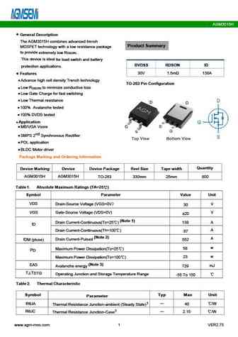
AGM3015H General Description The AGM3015H combines advanced trench Product Summary MOSFET technology with a low resistance package to provide extremely low R . DS(ON) This device is ideal for load switch and battery BVDSS RDSON ID protection applications. 30V 1.5m 138A Features Advance high cell density Trench technology TO-263 Pin Configuration Low R to mini... See More ⇒
agm30p25s.pdf
AGM30P25S Characteristics Curve Typ. output characteristics Typ. drain-source on resistance I =f(V ) R =f(I ) D DS DS(on) D Typ. transfer characteristics Drain-source on-state resistance I =f(V ) R =f(T );I =-5A; V =-10V D GS DS(on) j D GS www.agm-mos.com 3 VER2.5 AGM30P25S Gate Threshold Voltage Drain-source breakdown voltage -V =f(T ); I =-250uA V =f(T ); I =-250uA TH... See More ⇒
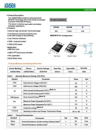
agm306mnq.pdf
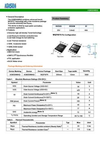
AGM306MNQ Table 3. Electrical Characteristics (TJ=25 unless otherwise noted) Symbol Parameter Conditions Min Typ Max Unit On/Off States BVDSS Drain-Source Breakdown Voltage V =0V I =250 A GS D 30 -- -- V Zero Gate Voltage Drain Current V =30V,V =0V -- -- 1 A DS GS I DSS Gate-Body Leakage Current V = 20V,V =0V -- -- nA GS DS I GSS 100 VGS(th) Gate Threshold Voltage V... See More ⇒
agm30p10a.pdf
AGM30P10A Fig.1 Power Dissipation Derating Curve Fig.2 Typical output Characteristics 1.2 50 VGS=-10V 1 40 0.8 30 VGS=-4.5V 0.6 20 0.4 10 0.2 0 0 0.5 1 0 Drain-Source voltage (V) 0 50 100 150 200 Temperature ( C) Fig.3 Threshold Voltage V.S Junction Temperature Fig.4 Resistance V.S Drain Current Junction Temperature 30 -50 50 150 0 20 -0.... See More ⇒
agm308mn.pdf
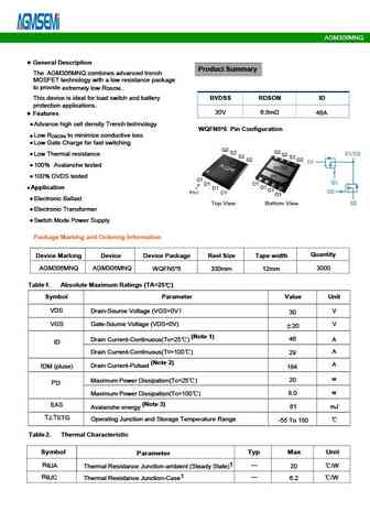
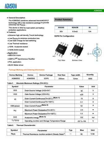
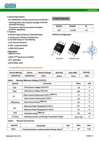
AGM308MN General Description The AGM308MN combines advanced trench Product Summary MOSFET technology with a low resistance package to provide extremely low R . DS(ON) This device is ideal for load switch and battery protection applications. BVDSS RDSON ID Features 30V 8.8m 15A Advance high cell density Trench technology Low R to minimize conductive loss DS(ON) ... See More ⇒
agm305a.pdf
AGM305A Typical electrical and thermal characteristics Figure 2 Typical Transfer Characteristics Figure 1 Typical Output Characteristics Figure 4 On-Resistance vs. Junction Figure 3 Body-Diode Characteristics Temperature Figure 5 Capacitance Characteristics Figure 6 Gate-Charge Characteristics www.agm-mos.com 3 VER2.72 AGM305A Test circuits and Waveforms Gate charge cir... See More ⇒
agm30p12d.pdf
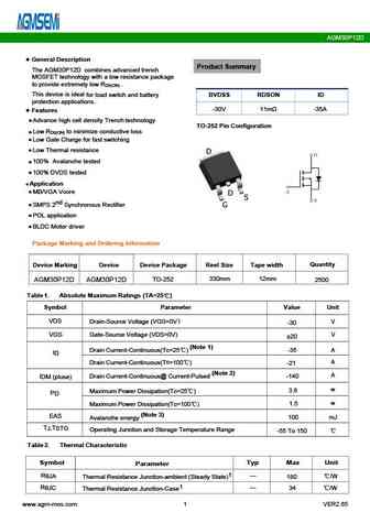
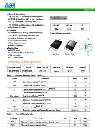
AGM30P12D General Description Product Summary The AGM30P12D combines advanced trench MOSFET technology with a low resistance package to provide extremely low R . DS(ON) This device is ideal for load switch and battery BVDSS RDSON ID protection applications. -30V 11m -35A Features Advance high cell density Trench technology TO-252 Pin Configuration Low R to minim... See More ⇒
agm306ap.pdf
AGM306AP Typical Characteristics 12 12 VGS=10V ID=12A VGS=7V 10 VGS=5V 11 8 VGS=4.5V VGS=3V 9 6 4 8 2 6 0 2 4 6 8 10 0 0.25 0.5 0.75 VGS (V) VDS Drain-to-Source Voltage (V) Fig.1 Typical Output Characteristics Fig.2 On-Resistance vs. Gate-Source 10 12 VDS=20V ID=12A 10 8 8 6 TJ=150 TJ=25 6 4 4 2 2 0 0 0 0.3 0.6 0.9 0 6 12 18 24 30 QG , Total Gate... See More ⇒
agm304mnq.pdf
AGM304MNQ Typical Characteristics Fig.1 Typical Output Characteristics Fig.2 On-Resistance vs G-S Voltage Fig.3 Source Drain Forward Characteristics Fig.4 Gate-Charge Characteristics 1.8 1.8 1.4 1.4 1.0 1 0.6 0.6 0.2 0.2 -50 0 50 100 150 -50 0 50 100 150 TJ ,Junction Temperature ( ) TJ , Junction Temperature ( ) Fig.5 Normalized V vs T Fig.6 Normalized R vs T GS(th) ... See More ⇒
agm30p25mbq.pdf
AGM30P25MBQ Table 2. P-Channel Electrical Characteristics (TJ=25 unless otherwisenoted) Symbol Parameter Conditions Min Typ Max Unit On/Off States BVDSS Drain-Source Breakdown Voltage VGS=0V ID=-250 A -30 -- -- V Zero Gate Voltage Drain Current V =-30V,V =0V -1 DS GS I -- -- A DSS Gate-Body Leakage Current V = 20V,V =0V 100 GS DS I -- -- nA GSS V Gate Threshold Voltage V... See More ⇒
agm308s.pdf
AGM308S Fig.1 Power Dissipation Fig.2 Typical output Characteristics V =10V GS V =4.5V GS Fig.3 Threshold Voltage V.S Junction Temperature Fig.4 Resistance V.S Drain Current Fig.5 On-Resistance VS Gate Source Voltage Fig.6 On-Resistance V.S Junction Temperature www.agm-mos.com 3 VER2.71 AGM308S Fig.7 Switching Time Measurement Circuit Fig.8 Gate Charge Waveform Fig.9 Switching Tim... See More ⇒
agm30p05ap.pdf
AGM30P05AP General Description The AGM30P05AP combines advanced trench Product Summary MOSFET technology with a low resistance package to provide extremely low R . DS(ON) This device is ideal for load switch and battery protection applications. BVDSS RDSON ID Features -30V 5.5m -60A Advance high cell density Trench technology Low R to minimize conductive loss D... See More ⇒
agm304ap.pdf
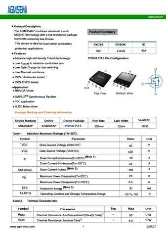
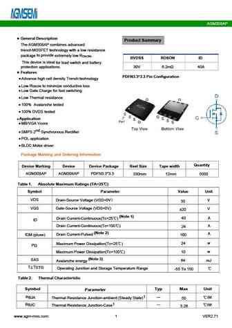
AGM304AP General Description The AGM304AP combines advanced trench Product Summary MOSFETtechnology with a low resistance package to provide extremely low R . DS(ON) This device is ideal for load switch and battery BVDSS RDSON ID protection applications. 30V 3.8m 40A Features Advance high cell density Trench technology PDFN3.3*3.3 Pin Configuration Low R to mi... See More ⇒
agm30p20m.pdf
AGM30P20M Characteristics Curve Typ. output characteristics Typ. drain-source on resistance -I =f(-V ) R =f(-I ) D DS DS(on) D Typ. transfer characteristics Drain-source on-state resistance -I =f(-V ) R = f(T ); I =-8A; V =-10V D GS DS(on) j D GS www.agm-mos.com 3 VER2.7 AGM30P20M Gate Threshold Voltage Drain-source breakdown voltage -V =f(T ); I =-250uA -V =f(T ); I =-2... See More ⇒
agm30p110d.pdf
AGM30P110D Table 3. Electrical Characteristics (TJ=25 unless otherwise noted) Symbol Parameter Conditions Min Typ Max Unit On/Off States BVDSS Drain-Source Breakdown Voltage V =0V I =-250 A -30 -- -- V GS D Zero Gate Voltage Drain Current V =-30V,V =0V -- -- -1 A DS GS I DSS Gate-Body Leakage Current V = 20V,V =0V -- -- 100 nA GS DS I GSS VGS(th) Gate Threshold Voltage... See More ⇒
agm308a.pdf
AGM308A Typical Performance Characteristics Figure 2 Typical Transfer Characteristics Figure1 Output Characteristics ID (A) ID (A) 100 100 10V 8V 80 80 3.5V 5V 60 60 40 40 3V 125 25 20 20 VGS=2.5V VGS(V) VDS(V) 0 0 0 2.0 4.0 6.0 8.0 10.0 0 1 2 3 4 5 6 Figure 3 On-resistance vs. Drain Current Figure 4 Body Diode Characteristics IS(A) RDS(ON) (m ) 14 10... See More ⇒
agm30p35s.pdf
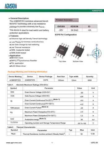
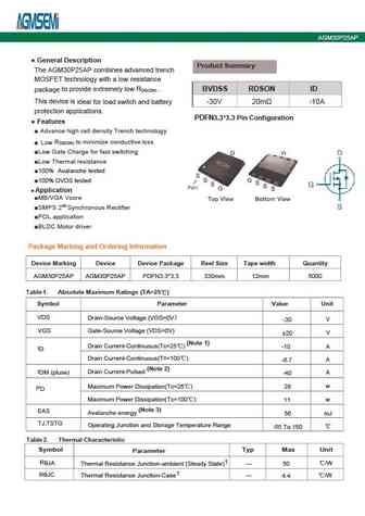
AGM30P35S General Description Product Summary The AGM30P35S combines advanced trench MOSFET technology with a low resistance to provide extremely low R . BVDSS RDSON ID package DS(ON) This device is ideal for load switch and battery -30V 34.5m -6A protection applications. SOP8 Pin Configuration Features Advance high cell density Trench technology R to minimize conduct... See More ⇒
agm30p35m.pdf
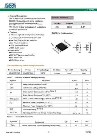
AGM30P35M General Description Product Summary The AGM30P35M combines advanced trench MOSFET technology with a low resistance to provide extremely low R . BVDSS RDSON ID package DS(ON) This device is ideal for load switch and battery -30V 33m -5.4A protection applications. Features SOP8 Pin Configuration Advance high cell density Trench technology R to minimize conduct... See More ⇒
agm30p100d.pdf
AGM30P100D Typical Characteristics -VDS,- Drain -Source Voltage (V) Tj - Junction Temperature ( C) Fig1. Typical Output Characteristics Fig2. -V Gate -Source Voltage Vs.Tj GS(TH) -VGS, -Gate -Source Voltage (V) Tj - Junction Temperature ( C) Fig3. Typical Transfer Characteristics Fig4. Normalized On-Resistance Vs. Tj -VSD, -Source-Drain Voltage (V) -VDS, -Drain -Source Vo... See More ⇒
agm306d.pdf
AGM306D Test Circuit 1) EAS Test Circuits 2) Gate Charge Test Circuit 3) Switch Time Test Circuit www.agm-mos.com 3 VER2.71 AGM306D TYPICAL ELECTRICAL AND THERMAL CHARACTERISTICS (Curves) Figure 1. Output Characteristics Figure 2. Transfer Characteristics VDS Drain-to-Source Voltage(V) VGS Gate-to-Source Voltage(V) Figure 3. Max BV vs Junction Temperature Figure 4. Drain Curren... See More ⇒
agm30p25ap.pdf
AGM30P25AP Table 2. P-Channel Electrical Characteristics (TJ=25 unless otherwisenoted) Symbol Parameter Conditions Min Typ Max Unit On/Off States BVDSS Drain-Source Breakdown Voltage VGS=0V ID=-250 A -30 -- -- V Zero Gate Voltage Drain Current V =-30V,V =0V -1 DS GS I -- -- A DSS Gate-Body Leakage Current V = 20V,V =0V 100 GS DS I -- -- nA GSS V Gate Threshold Voltage V ... See More ⇒
agm306mbq.pdf
AGM306MBQ Table 3. Electrical Characteristics (T =25 unless otherwise noted) J Symbol Parameter Conditions Min Typ Max Unit On/Off States BV Drain-Source Breakdown Voltage V =0V I =250 A 30 -- -- V GS D DSS Zero Gate Voltage Drain Current V =30V,V =0V -- -- 1 A DS GS I DSS Gate-Body Leakage Current V = 20V,V =0V -- -- nA GS DS I GSS 100 V Gate Threshold Voltage V =V ... See More ⇒
agm3045a.pdf
AGM3045A General Description Product Summary The AGM3045A combines advanced trench MOSFET to technology with a low resistance package provide extremely low R . DS(ON) BVDSS RDSON ID This device is ideal load switch and battery protection for applications. 30V 4.6m 80A Features Advance high cell density Trench technology PDFN5*6 Pin Configuration Low R to mini... See More ⇒
agm306c.pdf
AGM306C General Description Product Summary The AGM306C combines advanced trenchMOSFET to provide technology with a low resistance package extremely low R . DS(ON) This device is ideal BVDSS RDSON ID for load switch and battery protection applications. 30V 5.7m 60A Features Advance high cell density Trench technology TO-220 Pin Configuration Low R to minimize c... See More ⇒
agm304a.pdf
AGM304A General Description Product Summary The AGM304A combines advanced trench MOSFET to provide technology with a low resistance package extremely low R . DS(ON) This device is ideal for load switch and battery BVDSS RDSON ID protection applications. 30V 2.8m 100A Features PDFN5*6 Pin Configuration Advance high cell density Trench technology Low R to minimi... See More ⇒
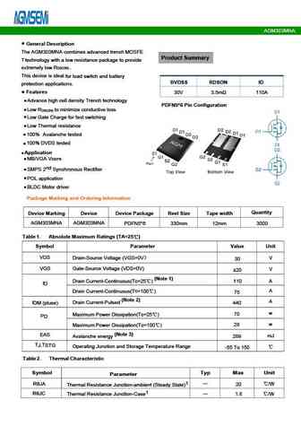
agm306mna.pdf
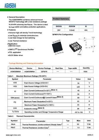
AGM306MNA General Description Product Summary The AGM306MNA combines advanced trench MOSFET technology with a low resistance package to provide extremely low R . This device is ideal DS(ON) BVDSS RDSON ID switch and battery protection applications. for load Features 30V 6.8m 40A Advance high cell density Trench technology QFN5*6 Pin Configuration Low R to minim... See More ⇒
agm308mar.pdf
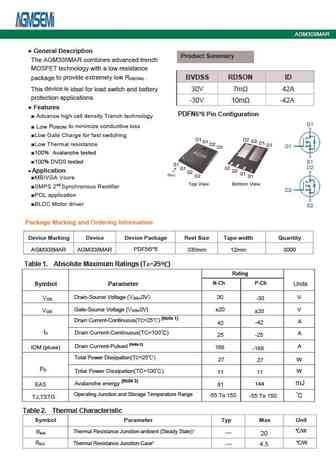
AGM308MAR Table 3. N- Channel Electrical Characteristics (TJ=25 unless otherwisenoted) Symbol Parameter Conditions Min Typ Max Unit On/Off States BV Drain-Source Breakdown Voltage V =0V I =250 A 30 -- -- V GS D DSS Zero Gate Voltage Drain Current V =30V,V =0V -- -- 1 A DS GS I DSS Gate-Body Leakage Current V = 20V,V =0V -- -- nA GS DS 100 I GSS VGS(th) Gate Threshold V... See More ⇒
agm303mna.pdf
AGM303MNA V =10V GS V =4.5V GS Fig.3 Threshold Voltage V.S Junction Temperature Fig.4 Resistance V.S Drain Current Fig.5 On-Resistance VS Gate Source Voltage Fig.6 On-Resistance V.S Junction Temperature www.agm-mos.com 3 VER2.5 AGM303MNA Fig.9 Switching Time Measurement Circuit Fig.10 Gate Charge Waveform Fig.11 Avalanche Measurement Circuit Fig.12 Avalanche Waveform www.agm-mos.c... See More ⇒
agm307mnq.pdf
AGM307MNQ Typical Characteristics VDS, Drain -Source Voltage (V) Tj - Junction Temperature ( C) Fig1. Typical Output Characteristics Fig2. Threshold Voltage Vs. Temperature VGS, Gate -Source Voltage (V) Tj - Junction Temperature ( C) Fig3. Typical Transfer Characteristics Fig4. Normalized On-Resistance Vs. Temperature VSD, Source-Drain Voltage (V) VDS, Drain -Source Voltage... See More ⇒
agm30p100a.pdf
AGM30P100A Typical Characteristics -VDS,- Drain -Source Voltage (V) Tj - Junction Temperature ( C) Fig1. Typical Output Characteristics Fig2. -V Gate -Source Voltage Vs.Tj GS(TH) -VGS, -Gate -Source Voltage (V) Tj - Junction Temperature ( C) Fig3. Typical Transfer Characteristics Fig4. Normalized On-Resistance Vs. Tj -VSD, -Source-Drain Voltage (V) -VDS, -Drain -Source Vo... See More ⇒
agm30p85d.pdf
AGM30P85D Table 3. Electrical Characteristics (TJ=25 unless otherwise noted) Symbol Parameter Conditions Min Typ Max Unit On/Off States BV Drain-Source Breakdown Voltage V =0V I =250 A -30 -- -- V GS D DSS Zero Gate Voltage Drain Current V =-30V,V =0V -- -- -1.0 A DS GS I DSS V = 20V,V =0V -- -- nA GS DS IGSS Gate-Body Leakage Current 100 V Gate Threshold Voltage V ... See More ⇒
agm303ap.pdf
AGM303AP Typical Characteristics VDS, Drain -Source Voltage (V) Tj - Junction Temperature ( C) Fig1. Typical Output Characteristics Fig2. V Gate -Source Voltage Vs.Tj GS(TH) VGS, Gate -Source Voltage (V) Tj - Junction Temperature ( C) Fig3. Typical Transfer Characteristics Fig4. Normalized On-Resistance Vs. Tj VSD, Source-Drain Voltage (V) VDS, Drain -Source Voltage (V) Fig5. Typica... See More ⇒
agm3015d.pdf
AGM3015D Typical Electrical and Thermal Characteristics (Curves) Vds Drain-Source Voltage (V) TJ-Junction Temperature( ) Figure 1 Output Characteristics Figure 4 Rdson-JunctionTemperature Vgs Gate-Source Voltage (V) Qg Gate Charge (nC) Figure 2 Transfer Characteristics Figure 5 Gate Charge ID- Drain Current (A) Vsd Source-Drain Voltage (V) Figure 3 Rdson- Drain Current Figure 6... See More ⇒
agm3015a.pdf
AGM3015A Typical Electrical & Thermal Characteristics 150 30 VGS = 10V VGS = 3.5V VDS = 5.0V VGS = 5.0V VGS = 4.5V 120 24 VGS = 4.0V TJ = 125 C 90 18 60 12 VGS = 3.0V TJ = 25 C 30 6 VGS = 2.7V VGS = 2.5V 0 0 0 0.6 1.2 1.8 2.4 3 1 1.5 2 2.5 3 3.5 VDS (V) VGS (V) Figure 1 Saturation Characteristics Figure 2 Transfer Characteristics 4 2.5 3.2 2 VGS = 10V ID = 20A VG... See More ⇒
agm308mbp.pdf
AGM308MBP Table 3. Electrical Characteristics (TJ=25 unless otherwise noted) Symbol Parameter Conditions Min Typ Max Unit On/Off States BVDSS Drain-Source Breakdown Voltage V =0V I =250 A 30 -- -- V GS D Zero Gate Voltage Drain Current V =30V,V =0V -- -- 1 A DS GS I DSS V = 20V,V =0V -- -- nA GS DS IGSS Gate-Body Leakage Current 100 VGS(th) Gate Threshold Voltage V =V... See More ⇒
agm307mbp.pdf
AGM307MBP Table 3. Electrical Characteristics (TJ=25 unless otherwise noted) Symbol Parameter Conditions Min Typ Max Unit On/Off States BVDSS Drain-Source Breakdown Voltage V =0V I =250 A 30 -- -- V GS D Zero Gate Voltage Drain Current V =30V,V =0V -- -- 1 A DS GS I DSS V = 20V,V =0V -- -- nA GS DS IGSS Gate-Body Leakage Current 100 VGS(th) Gate Threshold Voltage V =V... See More ⇒
agm30p18s.pdf
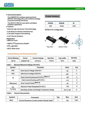
AGM30P18S General Description Product Summary The AGM30P18S combines advanced trench MOSFET technology with a low resistance package to provide extremely low R . DS(ON) This device is ideal for load switch and battery BVDSS RDSON ID protection applications. -30V 7.0m -17A Features Advance high cell density Trench technology SOP8 Pin Configuration Low R to minimi... See More ⇒
agm30p35ap.pdf
AGM30P35AP General Description Product Summary The AGM30P35AP combines advanced trench MOSFET technology with a low resistance to provide extremely low R . BVDSS RDSON ID package DS(ON) This device is ideal for load switch and battery -30V 34.5m -16A protection applications. PDFN3.3*3.3 Pin Configuration Features Advance high cell density Trench technology R to minimi... See More ⇒
agm304s.pdf
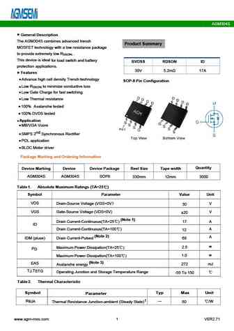
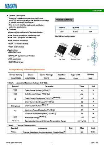
AGM304S General Description The AGM304S combines advanced trench Product Summary MOSFET technology with a low resistance package to provide extremely low R . DS(ON) This device is ideal for load switch and battery BVDSS RDSON ID protection applications. 30V 5.2m 17A Features Advance high cell density Trench technology SOP-8 Pin Configuration Low R to minimize... See More ⇒
agm30p08ap.pdf
AGM30P08AP P- Channel Typical Characteristics TC=25 impulse=250uS -4.5V -6V -10V -3.5V 25 -3V -2.5 V -Vds Drain-Source Voltage (V) -Vgs Gate-Source Voltage (V) Figure 1. On-Region Characteristics Figure 2. Transfer Characteristics Note TJ=25 VGS= 0V 25 VGS= -4.5V VGS= -10V -ID - Drain Current (A) -VF ,Forward Voltage (V) Figure 3. On-Resistance Variation vs F... See More ⇒
agm301c1.pdf
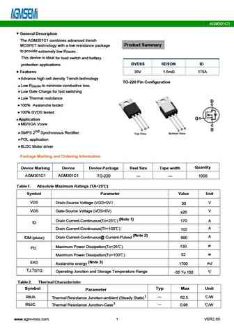
AGM301C1 General Description The AGM301C1 combines advanced trench Product Summary MOSFET technology with a low resistance package to provide extremely low R . DS(ON) This device is ideal for load switch and battery BVDSS RDSON ID protection applications. Features 30V 1.5m 170A Advance high cell density Trench technology TO-220 Pin Configuration Low R to minim... See More ⇒
agm3005a.pdf
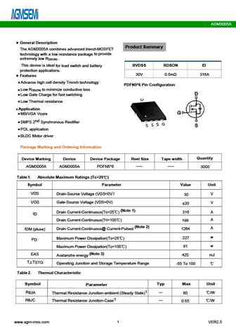
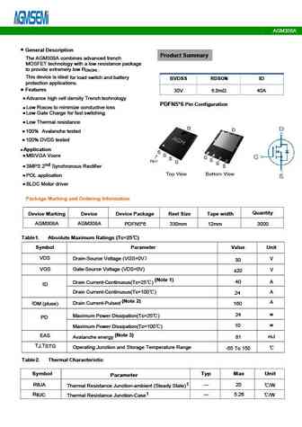
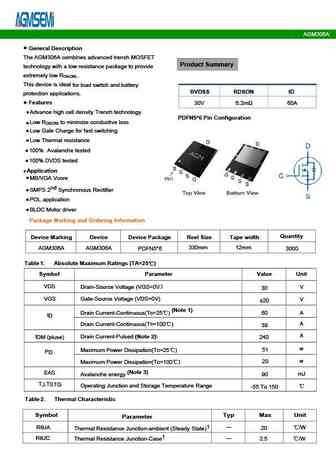
AGM3005A General Description Product Summary The AGM3005A combines advanced trenchMOSFET to provide technology with a low resistance package extremely low R . DS(ON) This device is ideal BVDSS RDSON ID for load switch and battery protection applications. 30V 0.5m 316A Features Advance high cell density Trench technology PDFN5*6 Pin Configuration Low R to minimi... See More ⇒
agm30p20d.pdf
AGM30P20D Table 3. Electrical Characteristics (TJ=25 unless otherwise noted) Symbol Parameter Conditions Min Typ Max Unit On/Off States BVDSS Drain-Source Breakdown Voltage V =0V I =-250 A -30 -- -- V GS D Zero Gate Voltage Drain Current V =-30V,V =0V -- -- -1 A DS GS I DSS Gate-Body Leakage Current V = 20V,V =0V -- -- 100 nA GS DS I GSS VGS(th) Gate Threshold Voltage ... See More ⇒
agm30p08d.pdf
AGM30P08D Table 3. Electrical Characteristics (TJ=25 unless otherwise noted) Symbol Parameter Conditions Min Typ Max Unit On/Off States BV Drain-Source Breakdown Voltage V =0V I =250 A -30 -- -- V GS D DSS Zero Gate Voltage Drain Current V =-30V,V =0V -- -- -1.0 A DS GS I DSS V = 20V,V =0V -- -- nA GS DS IGSS Gate-Body Leakage Current 100 V Gate Threshold Voltage V ... See More ⇒
agm30p25m.pdf
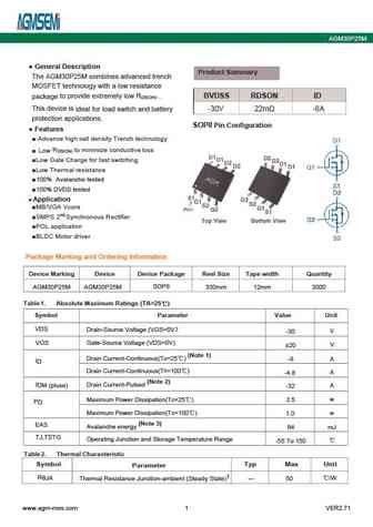
AGM30P25M General Description Product Summary The AGM30P25M combines advanced trench MOSFET technology with a low resistance to provide extremely low R . BVDSS RDSON ID package DS(ON) This device is ideal for load switch and battery -30V 22m -8A protection applications. SOP8 Pin Configuration Features Advance high cell density Trench technology R to minimize conductiv... See More ⇒
agm304ap-b.pdf
AGM304AP-B TYPICAL ELECTRICAL AND THERMAL CHARACTERIS Figure 2 Transfer Characteristics (Note E) Figure 1 On-Region Characteristics (Note E) Figure 4 On-Resistance vs. Junction Figure 3 On-Resistance vs. Drain Current and Gate Voltage (Note E) Temperature (Note E) Figure 5 On-Resistance vs. Gate-Source Figure 6 Body-Diode Characteristics (Note E) Voltage (Note E) www.agm... See More ⇒
agm30p10sr.pdf
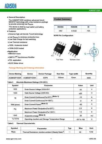
AGM30P10SR General Description Product Summary The AGM30P10SR combines advanced trench MOSFET technology with a low resistance package to provide extremely low R . DS(ON) This device is ideal for load switch and battery BVDSS RDSON ID protection applications. -30V 9.3m -15A Features Advance high cell density Trench technology SOP8 Pin Configuration Low R to mini... See More ⇒
agm30p25d.pdf
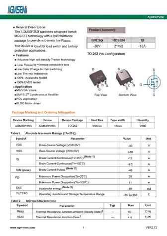
AGM30P25D General Description Product Summary The AGM30P25D combines advanced trench MOSFET technology with a low resistance to provide extremely low R . BVDSS RDSON ID package DS(ON) This device is ideal for load switch and battery -30V 21m -12A protection applications. TO-252 Pin Configuration Features Advance high cell density Trench technology R to minimize conduc... See More ⇒
agm30p110a.pdf
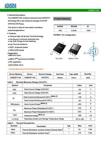
AGM30P110A Table 3. Electrical Characteristics (TJ=25 unless otherwise noted) Symbol Parameter Conditions Min Typ Max Unit On/Off States BVDSS Drain-Source Breakdown Voltage V =0V I =-250 A -30 -- -- V GS D Zero Gate Voltage Drain Current V =-30V,V =0V -- -- -1 A DS GS I DSS Gate-Body Leakage Current V = 20V,V =0V -- -- 100 nA GS DS I GSS VGS(th) Gate Threshold Voltage... See More ⇒
agm30p16s.pdf
AGM30P16S Ciss Vgs Coss Crss Qg Vds Fig.3 Power Dissipation Derating Curve Fig.4 Typical output Characteristics V =-10V GS V =-4.5V GS Fig.5 Threshold Voltage V.S Junction Temperature Fig.6 Resistance V.S Drain Current www.agm-mos.com 3 VER2.68 AGM30P16S Fig.9 Switching Time Measurement Circuit Fig.10 Gate Charge Waveform Fig.11 Switching Time Measurement Circuit Fig.12 Gate ... See More ⇒
agm30p55d1.pdf
AGM30P55D1 General Description Product Summary The AGM30P55D1 combines advanced trench MOSFET technology with a low resistance package to provide extremely low R . DS(ON) This device is ideal for load switch and battery BVDSS RDSON ID protection applications. -30V 6.5m -65A Features Advance high cell density Trench technology TO-252 Pin Configuration Low R to mi... See More ⇒
agm30p12m.pdf
AGM30P12M Fig.1 Power Dissipation Derating Curve Fig.2 Typical output Characteristics 1.2 50 VGS=-10V 1 40 0.8 30 VGS=-4.5V 0.6 20 0.4 10 0.2 0 0 0.5 1 0 Drain-Source voltage (V) 0 50 100 150 200 Temperature ( C) Fig.3 Threshold Voltage V.S Junction Temperature Fig.4 Resistance V.S Drain Current Junction Temperature 30 -50 50 150 0 20 -0.... See More ⇒
agm30p14mbp.pdf
AGM30P14MBP -Vds Drain-Source Voltage (V) TJ-Junction Temperature( ) Figure 7 Capacitance vs Vds Figure 9 Power De-rating -Vds Drain-Source Voltage (V) TJ-Junction Temperature( ) Figure 8 Safe Operation Area Figure 10 ID Current Derating Square Wave Pluse Duration(sec) Figure 11 Normalized Maximum Transient Thermal Impedance www.agm-mos.com 4 VER2.68 C Capacitance (pF) Po... See More ⇒
agm30p10k.pdf
AGM30P10K Typical Characteristics Power Capability Current Capability 60 55 50 50 45 40 40 35 30 30 25 20 20 15 10 10 5 TC=25oC,VG= -10V TC=25oC 0 0 0 20 40 60 80 100 120 140 160 180 0 20 40 60 80 100 120 140 160 Tmp Mounting Point Temp. ( Tmp Mounting Point Temp. ( C) C) Safe Operating Area Transient Thermal Impedance 100 2 1 Duty = 0.5 1ms 0.2 ... See More ⇒
agm30p20ap.pdf
AGM30P20AP Characteristics Curve www.agm-mos.com 3 VER2.68 AGM30P20AP Figure7 Safe Operation Area Figure8 Normalized Maximum Transient Thermal Impedance www.agm-mos.com 4 VER2.68 AGM30P20AP Dimensions PDFN3.3*3.3 MILLIMETER D SYMBOL MIN Typ. MAX A 0.700 0.800 0.900 b A1 0.152REF. A2 0 0.05 D 3.000 3.100 3.200 D1 2.300 2.450 2.600 D1 E 2.900 3.000 3.100 E1 3.1... See More ⇒
agm308ap.pdf
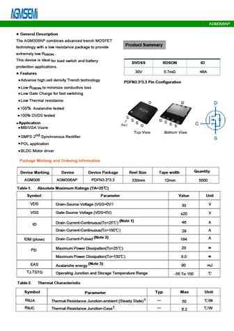
AGM308AP General Description Product Summary The AGM308AP combines advanced trenchMOSFET technology with a low resistance to provide package extremely low R . DS(ON) BVDSS RDSON ID This device is ideal for load switch and battery 30V 6.2m 40A protection applications. Features PDFN3.3*3.3 Pin Configuration Advance high cell density Trench technology Low R to mi... See More ⇒
agm305ma.pdf
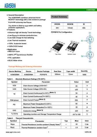
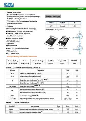
AGM305MA General Description Product Summary The AGM305MA combines advanced trench MOSFET technology with a low resistance package to provide extremely low R . DS(ON) BVDSS RDSON ID switch and battery This device is ideal for load protection applications. 30V 4.6m 50A Features PDFN5*6 Pin Configuration Advance high cell density Trench technology Low R to minim... See More ⇒
agm304d.pdf
AGM304D Typical Characteristics TJ = 25 C, unless otherwise noted 120 120 10V 8V 100 100 6V VDS = 15V 4.5V 4V 80 80 3.5V 60 60 40 40 C 20 TJ = 125 20 TJ = 25 C 0 0 0 1 2 3 4 5 0 1 2 3 4 5 6 VDS (Volts) VGS (Volts) Figure 1 On-Region Characteristics Figure 2 Transfer Characteristics 10000 10 9 TJ = 25 C 8 Ciss 1000 7 VGS = 4.5V Co... See More ⇒
agm30p10ap.pdf
AGM30P10AP P- Channel Typical Characteristics -3V TC=25 impulse=250uS -3.5V -4.5V 25 -6V -10V -2.5V Vds Drain-Source Voltage (V) -Vgs Gate-Source Voltage (V) Figure 1. On-Region Characteristics Figure 2. Transfer Characteristics VGS= 0V Note TJ=25 VGS=-4.5V 25 VGS=-10V -V F ,Forward Voltage [V] -I D - Drain Current (A) Figure 4. Body Diode Forward Voltage F... See More ⇒
agm306ma.pdf
AGM306MA Fig.1 Power Dissipation Derating Curve Fig.2 Typical output Characteristics 1.2 50 1 V =10V GS 0.8 V =4.5V GS 25 0.6 0.4 0.2 0 0 0.5 1 1.5 2 0 Drain-Source voltage (V) 0 50 100 150 200 Temperature ( C) Fig.3 Threshold Voltage V.S Junction Temperature Fig.4 Resistance V.S Drain Current 2.5 20 2 1.5 10 1 0.5 0 0 -50 50 150 0 10 20 30 Junction Tempe... See More ⇒
agm30p18e.pdf
AGM30P18E Table 3. Electrical Characteristics (TA=25 unless otherwise noted) Symbol Parameter Conditions Min Typ Max Unit On/Off States BV Drain-Source Breakdown Voltage V =0V I =250 A -30 -- -- V GS D DSS Zero Gate Voltage Drain Current V =-30V,V =0V -- -- -1 A DS GS I DSS V = 20V,V =0V -- -- nA GS DS IGSS Gate-Body Leakage Current 100 VGS(th) Gate Threshold Voltag... See More ⇒
agm3012ap-cp.pdf
AGM3012AP-CP Table 3. Electrical Characteristics (TJ=25 unless otherwise noted) Symbol Parameter Conditions Min Typ Max Unit On/Off States BV Drain-Source Breakdown Voltage V =0V I =250 A 30 35 -- V GS D DSS Zero Gate Voltage Drain Current V =30V,V =0V -- -- 1 A DS GS I DSS V = 20V,V =0V -- -- nA GS DS IGSS Gate-Body Leakage Current 100 VGS(th) Gate Threshold Voltag... See More ⇒
agm30p16d.pdf
AGM30P16D Typical Electrical and Thermal Characteristics (Curves) -Vds Drain-Source Voltage (V) TJ-Junction Temperature( ) Figure 1 Output Characteristics Figure 4 Rdson-Junction Temperature Vgs Gate-Source Voltage (V) Qg Gate Charge (nC) Figure 2 Transfer Characteristics Figure 5 Gate Charge -ID- Drain Current (A) Vsd Source-Drain Voltage (V) Figure 3 Rdson- Drain Current Figu... See More ⇒
agm30p05d.pdf
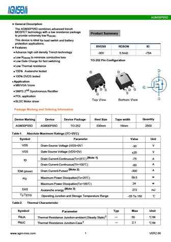
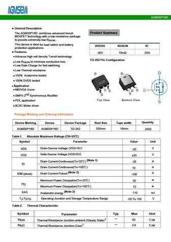
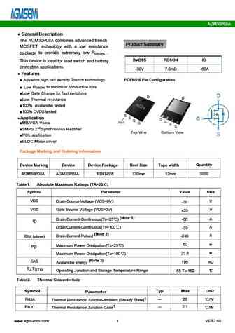
AGM30P05D General Description The AGM30P05D combines advanced trench MOSFET technology with a low resistance package Product Summary to provide extremely low R . DS(ON) This device is ideal for load switch and battery protection applications. BVDSS RDSON ID Features Advance high cell density Trench technology -30V 5.5m -75A Low R to minimize conductive loss DS(... See More ⇒
agm306a.pdf
AGM306A Table 3. Electrical Characteristics (T =25 unless otherwise noted) J Symbol Parameter Conditions Min Typ Max Unit On/Off States BV Drain-Source Breakdown Voltage V =0V I =250 A 30 -- -- V GS D DSS Zero Gate Voltage Drain Current V =30V,V =0V -- -- 1 A DS GS I DSS V = 20V,V =0V -- -- nA GS DS IGSS Gate-Body Leakage Current 100 VGS(th) Gate Threshold Voltage V... See More ⇒
agm30p05a.pdf
AGM30P05A General Description The AGM30P05A combines advanced trench Product Summary MOSFET technology with a low resistance package to provide extremely low R . DS(ON) This device is ideal for load switch and battery BVDSS RDSON ID protection applications. Features -30V 5.5m -75A Advance high cell density Trench technology PDFN5*6 Pin Configuration Low R to mi... See More ⇒
agm303a.pdf
AGM303A V =10V GS V =4.5V GS Fig.3 Threshold Voltage V.S Junction Temperature Fig.4 Resistance V.S Drain Current Fig.5 On-Resistance VS Gate Source Voltage Fig.6 On-Resistance V.S Junction Temperature www.agm-mos.com 3 VER2.72 AGM303A Fig.9 Switching Time Measurement Circuit Fig.10 Gate Charge Waveform Fig.11 Avalanche Measurement Circuit Fig.12 Avalanche Waveform www.agm-mos.com ... See More ⇒
agm306mbp.pdf
AGM306MBP Table 3. Electrical Characteristics (T =25 unless otherwise noted) J Symbol Parameter Conditions Min Typ Max Unit On/Off States BV Drain-Source Breakdown Voltage V =0V I =250 A 30 -- -- V GS D DSS Zero Gate Voltage Drain Current V =30V,V =0V -- -- 1 A DS GS I DSS Gate-Body Leakage Current V = 20V,V =0V -- -- nA GS DS I GSS 100 V Gate Threshold Voltage V =V ... See More ⇒
agm30p08a.pdf
AGM30P08A General Description The AGM30P08A combines advanced trench Product Summary MOSFET technology with a low resistance to provide extremely low R . package DS(ON) BVDSS RDSON ID This device is ideal for load switch and battery protection applications. -30V 7.0m -60A Features Advance high cell density Trench technology PDFN5*6 Pin Configuration R to minimize con... See More ⇒
agm30p10s.pdf
AGM30P10S General Description Product Summary The AGM30P10S combines advanced trench MOSFET technology with a low resistance package to provide extremely low R . DS(ON) This device is ideal for load switch and battery BVDSS RDSON ID protection applications. -30V 12m -14A Features Advance high cell density Trench technology SOP8 Pin Configuration Low R to minimiz... See More ⇒
agm30p55d.pdf
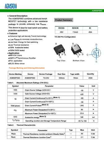
AGM30P55D General Description The AGM30P55D combines advanced trench Product Summary MOSFET technology with a low resistance package to provide extremely low R . DS(ON) This device is ideal for load switch and battery protection applications. BVDSS RDSON ID Features -30V 5m -65A Advance high cell density Trench technology Low R to minimize conductive loss DS(ON)... See More ⇒
agm30p16ap.pdf
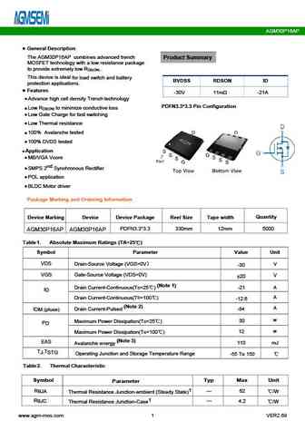
AGM30P16AP General Description The AGM30P16AP combines advanced trench Product Summary MOSFET technology with a low resistance package to provide extremely low R . DS(ON) This device is ideal for load switch and battery BVDSS RDSON ID protection applications. Features -30V 11m -21A Advance high cell density Trench technology PDFN3.3*3.3 Pin Configuration Low R ... See More ⇒
agm30p35d.pdf
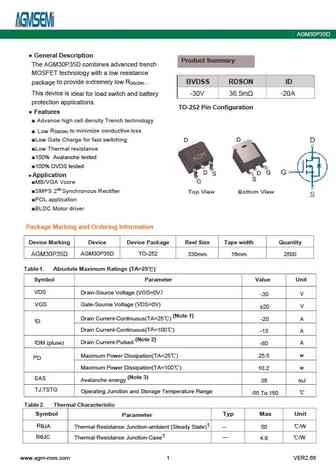
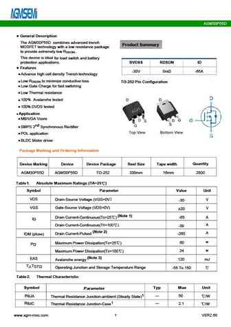
AGM30P35D General Description Product Summary The AGM30P35D combines advanced trench MOSFET technology with a low resistance to provide extremely low R . BVDSS RDSON ID package DS(ON) This device is ideal for load switch and battery -30V 36.5m -20A protection applications. TO-252 Pin Configuration Features Advance high cell density Trench technology R to minimize cond... See More ⇒
agm30p55a.pdf
AGM30P55A Fig.1 Power Dissipation Derating Curve Fig.2 Typical output Characteristics V =-10V GS V =-4.5V GS Fig.3 Threshold Voltage V.S Junction Temperature Fig.4 Resistance V.S Drain Current Fig.5 On-Resistance VS Gate Source Voltage Fig.6 On-Resistance V.S Junction Temperature www.agm-mos.com 3 VER2.68 AGM30P55A Fig.7 Switching Time Measurement Circuit Fig.8 Gate Charge Waveform... See More ⇒
agm303d.pdf
AGM303D V =10V GS V =4.5V GS Fig.3 Threshold Voltage V.S Junction Temperature Fig.4 Resistance V.S Drain Current Fig.5 On-Resistance VS Gate Source Voltage Fig.6 On-Resistance V.S Junction Temperature www.agm-mos.com 3 VER2.72 AGM303D Fig.9 Switching Time Measurement Circuit Fig.10 Gate Charge Waveform Fig.11 Avalanche Measurement Circuit Fig.12 Avalanche Waveform www.agm-mos.com ... See More ⇒
agm30p20s.pdf
AGM30P20S General Description Product Summary The AGM30P20S combines advanced trench MOSFET to provide technology with a low resistance package extremely low R DS(ON) BVDSS RDSON ID This device is ideal for load switch and battery protection applications. -30V 15.5m -11A Features Advance high cell density Trench technology SOP8 Pin Configuration Low R to minimize co... See More ⇒
agm301a1.pdf
AGM301A1 Table 3. Electrical Characteristics (T =25 unless otherwise noted) J Symbol Parameter Conditions Min Typ Max Unit On/Off States BV Drain-Source Breakdown Voltage V =0V I =250 A 30 -- -- V GS D DSS Zero Gate Voltage Drain Current V =30V,V =0V -- -- 1 A DS GS I DSS V = 20V,V =0V -- -- nA GS DS IGSS Gate-Body Leakage Current 100 VGS(th) Gate Threshold Voltage ... See More ⇒
agm305d.pdf
AGM305D www.agm-mos.com 3 VER2.71 AGM305D TYPICAL ELECTRICAL AND THERMAL CHARACTERISTICS (Curves) Figure 1. Output Characteristics Figure 2. Transfer Characteristics VDS Drain-to-Source Voltage(V) VGS Gate-to-Source Voltage(V) Figure 3. Max BVDSS vs Junction Temperature Figure 4. Drain Current TJ-Junction Temperature( ) TJ-Junction Temperature( ) Figure 5. VGS(th) vs Juncti... See More ⇒
agm304a-b.pdf
AGM304A-B TYPICAL ELECTRICAL AND THERMAL CHARACTERIS Figure 2 Transfer Characteristics (Note E) Figure 1 On-Region Characteristics (Note E) Figure 4 On-Resistance vs. Junction Figure 3 On-Resistance vs. Drain Current and Gate Voltage (Note E) Temperature (Note E) Figure 5 On-Resistance vs. Gate-Source Figure 6 Body-Diode Characteristics (Note E) Voltage (Note E) www.agm-... See More ⇒
agm308sr.pdf
AGM308SR Fig.1 Power Dissipation Fig.2 Typical output Characteristics 1.2 200 1 150 0.8 V =10V GS 100 0.6 V =4.5V GS 0.4 50 0.2 0 0 0.5 1 1.5 2 0 Drain-Source voltage (V) 0 50 100 150 200 Temperature ( C) Fig.3 Threshold Voltage V.S Junction Temperature Fig.4 Resistance V.S Drain Current 2.5 6 5 2 4 1.5 3 1 2 0.5 1 0 0 0 50 100 -50 50 150 Drain Curren... See More ⇒
Detailed specifications: AGM15T13D, AGM15T13F, AGM15T13H, AGM15T16C, AGM15T16D, AGM16N10C, AGM16N10D, AGM302C1, SKD502T, AGM303A, AGM303AP, AGM303D, AGM303D1, AGM303MNA, AGM3045A, AGM304A, AGM304A-B
Keywords - AGM302D1 MOSFET specs
AGM302D1 cross reference
AGM302D1 equivalent finder
AGM302D1 pdf lookup
AGM302D1 substitution
AGM302D1 replacement
Step-by-step guide to finding a MOSFET replacement. Cross-reference parts and ensure compatibility for your repair or project.
MOSFET Parameters. How They Affect Each Other
History: NDP4060 | AS3404 | NP52N06SLG | 2N7293 | FQP19N10 | AGM302C1 | APT10090SFLLG
🌐 : EN ES РУ

LIST
Last Update
MOSFET: CS95118 | CS85105A | CS75N45 | CS72N12 | CS55N50 | CS48N75A | CS40N27 | MSQ60P04D | MSQ40P07D | MSQ30P40D
Popular searches
c5198 | 2sc1969 transistor | bcy21 | s8550 datasheet | mj50ac100 | 2sc1318 replacement | 2n3905 | mj15023