AGM15N10D Datasheet. Specs and Replacement
Type Designator: AGM15N10D 📄📄
Type of Transistor: MOSFET
Type of Control Channel: N-Channel
Absolute Maximum Ratings
Pd ⓘ - Maximum Power Dissipation: 46 W
|Vds|ⓘ - Maximum Drain-Source Voltage: 100 V
|Vgs|ⓘ - Maximum Gate-Source Voltage: 20 V
|Id| ⓘ - Maximum Drain Current: 15 A
Tj ⓘ - Maximum Junction Temperature: 150 °C
Electrical Characteristics
tr ⓘ - Rise Time: 7 nS
Cossⓘ - Output Capacitance: 37 pF
RDSonⓘ - Maximum Drain-Source On-State Resistance: 0.1 Ohm
Package: TO252
📄📄 Copy
- MOSFET ⓘ Cross-Reference Search
AGM15N10D datasheet
..1. Size:806K cn agmsemi
agm15n10d.pdf 
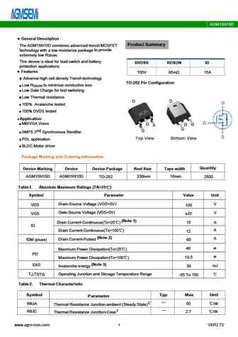
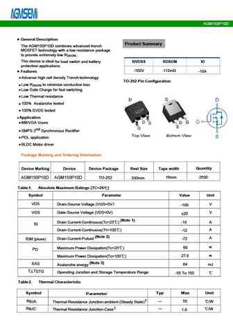
AGM15N10D General Description Product Summary The AGM15N10D combines advanced trench MOSFET to provide technology with a low resistance package extremely low R DS(ON) This device is ideal and battery for load switch BVDSS RDSON ID protection applications. Features 100V 85m 15A Advance high cell density Trench technology TO-252 Pin Configuration Low R to minimize co... See More ⇒
0.1. Size:1354K cn agmsemi
agm15n10d-g.pdf
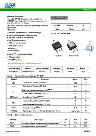
AGM15N10D-G General Description Product Summary The AGM15N10D-G combines advanced trench to MOSFET technology with a low resistance package provide extremely low R DS(ON) BVDSS RDSON ID This device is ideal for load switch and battery protection applications. 100V 68m 16A Features Advance high cell density Trench technology TO-252 Pin Configuration Low R to minimiz... See More ⇒
6.1. Size:1584K cn agmsemi
agm15n10ap.pdf
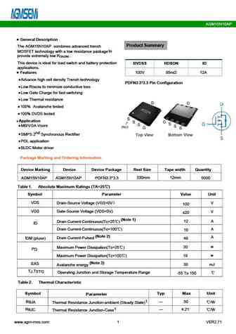
AGM15N10AP General Description Product Summary The AGM15N10AP combines advanced trench to MOSFET technology with a low resistance package provide extremely low R . DS(ON) This device is ideal load switch and battery protection for BVDSS RDSON ID applications. Features 100V 85m 12A Advance high cell density Trench technology PDFN3.3*3.3 Pin Configuration Low R ... See More ⇒
9.1. Size:924K cn agmsemi
agm15t16d.pdf
AGM15T16D Table 3. Electrical Characteristics (TJ=25 unless otherwise noted) Symbol Parameter Conditions Min Typ Max Unit On/Off States BVDSS Drain-Source Breakdown Voltage V =0V I =250 A GS D 150 -- -- V Zero Gate Voltage Drain Current V =150V,V =0V -- -- 1 A DS GS I DSS Gate-Body Leakage Current V = 20V,V =0V -- -- nA GS DS I GSS 100 VGS(th) Gate Threshold Voltage... See More ⇒
9.2. Size:1329K cn agmsemi
agm150p10s.pdf
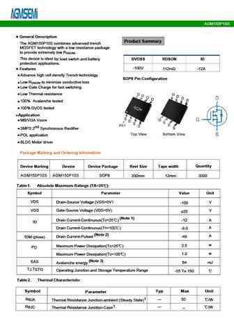
AGM150P10S Gate Threshold Voltage Drain-source breakdown voltage -V =f(T ); I =-250uA -V =f(T ); I =-250uA TH j D BR(DSS) j D Typ. gate charge Typ. capacitances -V =f(Q ) ; I =-5A C =f(-V ); V =0V; f =1MHz GS g D DS GS www.agm-mos.com 3 VER2.65 AGM150P10S Max. transient thermal impedance Z =f(t ) thJC p www.agm-mos.com 5 VER2.65 AGM150P10S Test Circuit and Waveform ... See More ⇒
9.3. Size:1311K cn agmsemi
agm15p13e.pdf
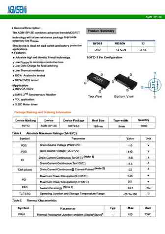
AGM15P13E Characteristics Curve Typ. output characteristics Typ. drain-source on resistance I =f(V ) R =f(I ) D DS DS(on) D Typ. transfer characteristics Drain-source on-state resistance I =f(V ) R =f(T );I =-5A; D GS DS(on) j D V =10V GS www.agm-mos.com 3 VER2.6 AGM15P13E Gate Threshold Voltage Drain-source breakdown voltage -V =f(T ); I =-250uA V =f(T ); I =-250uA ... See More ⇒
9.4. Size:1523K cn agmsemi
agm15t03ll.pdf
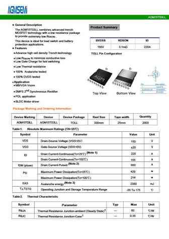
AGM15T03LL Fig 1. Typical Output Characteristics Figure 2. On-Resistance vs. Gate-Source Voltage 6V 100 8 ID=20A 10V 5V 80 6 4.5V 125 60 4 40 25 2 20 Vgs=4V 0 0 0 0.5 1 1.5 2 2 4 6 8 10 VDS (V) VGS (V) Figure 3. On-Resistance vs. Drain Current and Gate Voltage Figure 4. Normalized On-Resistance vs. Junction Temperature 7 2.6 ID=20A 2.4 6 2.2 VGS=10V 5 2 ... See More ⇒
9.5. Size:2043K cn agmsemi
agm15t06c-b.pdf
AGM15T06C-B Table 3. Electrical Characteristics (TJ=25 unless otherwise noted) Symbol Parameter Conditions Min Typ Max Unit On/Off States BV Drain-Source Breakdown Voltage V =0V I =250 A 140 147 -- V GS D DSS Zero Gate Voltage Drain Current V =140V,V =0V -- -- 1 A DS GS I DSS V = 20V,V =0V -- -- nA GS DS IGSS Gate-Body Leakage Current 100 VGS(th) Gate Threshold Volt... See More ⇒
9.6. Size:1200K cn agmsemi
agm15p22as.pdf
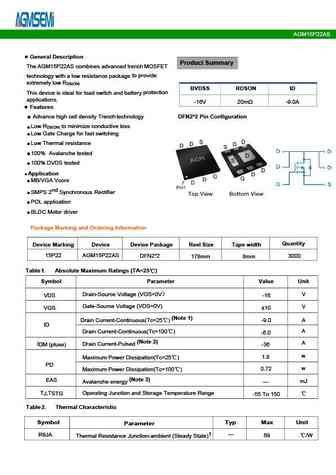
AGM15P22AS Table 3. Electrical Characteristics (TJ=25 unless otherwise noted) Symbol Parameter Conditions Min Typ Max Unit On/Off States BVDSS Drain-Source Breakdown Voltage V =0V I =-250 A -16 -- -- V GS D Zero Gate Voltage Drain Current V =-16V,V =0V -- -- -1 A DS GS I DSS Gate-Body Leakage Current V = 10V,V =0V -- -- 100 nA GS DS I GSS VGS(th) Gate Threshold Voltage... See More ⇒
9.7. Size:1270K cn agmsemi
agm15t16c.pdf
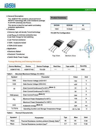
AGM15T16C Typical Electrical & Thermal Characteristics 100 30 VGS = 10V VDS = 5.0V VGS = 6.0V VGS = 8.0V 80 24 TJ = 125 C 60 18 VGS = 5.5V 40 12 TJ = 25 C VGS = 5.0V 20 6 VGS = 4.5V 0 0 0 1 2 3 4 5 2 3 4 5 6 7 VDS (V) VGS (V) Figure 1 Saturation Characteristics Figure 2 Transfer Characteristics 17 2.5 VGS = 10V ID = 20A 16 2 15 1.5 VGS = 10V 14 1 13 0.5 12 0 0... See More ⇒
9.8. Size:1243K cn agmsemi
agm150p10d.pdf
AGM150P10D Gate Threshold Voltage Drain-source breakdown voltage -V =f(T ); I =-250uA -V =f(T ); I =-250uA TH j D BR(DSS) j D Typ. gate charge Typ. capacitances -V =f(Q ) ; I =-5A C =f(-V ); V =0V; f =1MHz GS g D DS GS www.agm-mos.com 3 VER2.66 AGM150P10D Max. transient thermal impedance Z =f(t ) thJC p www.agm-mos.com 5 VER2.66 AGM150P10D Test Circuit and Waveform ... See More ⇒
9.9. Size:1357K cn agmsemi
agm15p16as.pdf
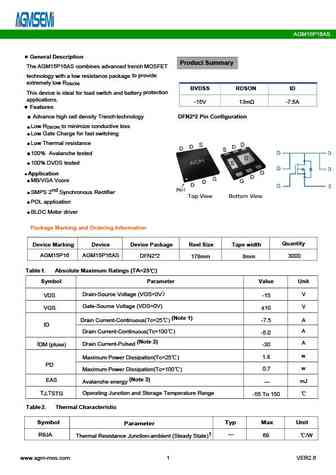
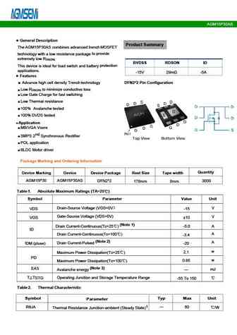
AGM15P16AS General Description Product Summary The AGM15P16AS combines advanced trench MOSFET to provide technology with a low resistance package extremely low R DS(ON) BVDSS RDSON ID protection This device is ideal for load switch and battery applications. -15V 13m -7.5A Features Advance high cell density Trench technology DFN2*2 Pin Configuration Low R to minimize... See More ⇒
9.10. Size:1224K cn agmsemi
agm15t13a.pdf
AGM15T13A Typical Electrical and Thermal Characteristics 150 150 VGS = 10V VDS = 5.0V 8.0V VGS = 6.0V 7.0V 120 120 VGS = 5.5V 90 90 TJ = 175 C VGS = 5.0V 60 60 VGS = 4.8V TJ = 25 C 30 30 VGS = 4.5V 0 0 0 2 4 6 8 10 0 1 2 3 4 5 VGS - Gate-to-Source Voltage (V) VDS - Drain-to-Source Voltage (V) Figure 2 Transfer Characteristics Figure 1 Output Characteristics 5... See More ⇒
9.11. Size:1020K cn agmsemi
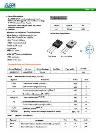
agm15t13h.pdf
AGM15T13H Table3. Electrical Characteristics (TJ=25 unless otherwise noted) Symbol Parameter Conditions Min Typ Max Unit On/Off States BV Drain-Source Breakdown Voltage V =0V I =250 A 150 -- V GS D DSS -- Zero Gate Voltage Drain Current V =150V,V =0V -- 1 A DS GS I -- DSS V = 20V,V =0V -- -- nA GS DS IGSS Gate-Body Leakage Current 100 V Gate Threshold Voltage V =V ... See More ⇒
9.12. Size:1457K cn agmsemi
agm15t06h.pdf
AGM15T06H Table 3. Electrical Characteristics (TJ=25 unless otherwise noted) Symbol Parameter Conditions Min Typ Max Unit On/Off States BVDSS Drain-Source Breakdown Voltage V =0V I =250 A 150 -- -- V GS D Zero Gate Voltage Drain Current V =150V,V =0V -- -- 1 A DS GS I DSS Gate-Body Leakage Current V = 20V,V =0V -- -- nA GS DS I GSS 100 VGS(th) Gate Threshold Voltage V... See More ⇒
9.13. Size:1401K cn agmsemi
agm15t06ll.pdf
AGM15T06LL Table 3. Electrical Characteristics (TJ=25 unless otherwise noted) Symbol Parameter Conditions Min Typ Max Unit On/Off States BVDSS Drain-Source Breakdown Voltage V =0V I =250 A 150 -- -- V GS D Zero Gate Voltage Drain Current V =150V,V =0V -- -- 1 A DS GS I DSS Gate-Body Leakage Current V = 20V,V =0V -- -- nA GS DS I GSS 100 VGS(th) Gate Threshold Voltage ... See More ⇒
9.14. Size:1601K cn agmsemi
agm15p30as.pdf
AGM15P30AS Table 3. Electrical Characteristics (TJ=25 unless otherwise noted) Symbol Parameter Conditions Min Typ Max Unit On/Off States BVDSS Drain-Source Breakdown Voltage V =0V I =-250 A -15 -18 -- V GS D Zero Gate Voltage Drain Current V =-15V,V =0V -- -- -1 A DS GS I DSS Gate-Body Leakage Current V = 10V,V =0V -- -- 100 nA GS DS I GSS VGS(th) Gate Threshold Voltag... See More ⇒
9.15. Size:1281K cn agmsemi
agm15p30e.pdf
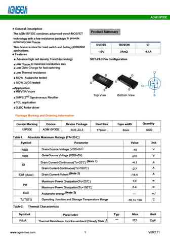
AGM15P30E General Description Product Summary The AGM15P30E combines advanced trench MOSFET to provide technology with a low resistance package extremely low R DS(ON) BVDSS RDSON ID protection This device is ideal for load switch and battery applications. -15V 34m -4.1A Features Advance high cell density Trench technology SOT-23-3 Pin Configuration Low R to minimize... See More ⇒
9.16. Size:1427K cn agmsemi
agm15t06t.pdf
AGM15T06T Table 3. Electrical Characteristics (TJ=25 unless otherwise noted) Symbol Parameter Conditions Min Typ Max Unit On/Off States BVDSS Drain-Source Breakdown Voltage V =0V I =250 A 150 -- -- V GS D Zero Gate Voltage Drain Current V =150V,V =0V -- -- 1 A DS GS I DSS Gate-Body Leakage Current V = 20V,V =0V -- -- nA GS DS I GSS 100 VGS(th) Gate Threshold Voltage V... See More ⇒
9.17. Size:1496K cn agmsemi
agm15t06c.pdf
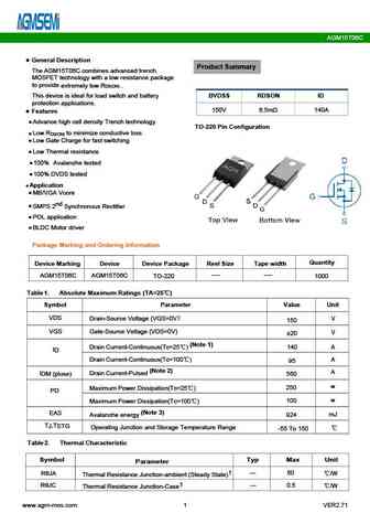
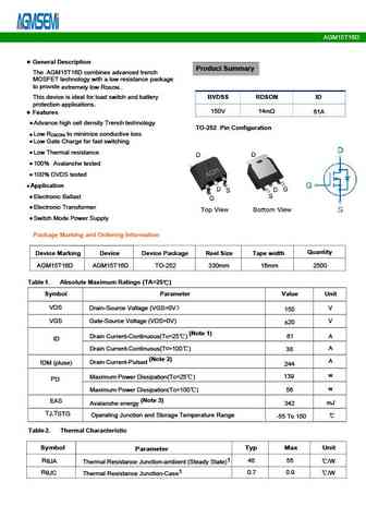
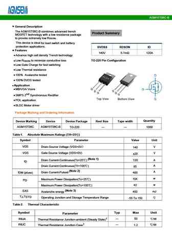
AGM15T06C General Description Product Summary The AGM15T06C combines advanced trench MOSFET technology with a low resistance package to provide extremely low R . DS(ON) This device is ideal switch and battery BVDSS RDSON ID for load protection applications. 150V 6.5m 140A Features Advance high cell density Trench technology TO-220 Pin Configuration Low R to mi... See More ⇒
9.18. Size:1035K cn agmsemi
agm15t13d.pdf
AGM15T13D Table3. Electrical Characteristics (TJ=25 unless otherwise noted) Symbol Parameter Conditions Min Typ Max Unit On/Off States BV Drain-Source Breakdown Voltage V =0V I =250 A 150 -- V GS D DSS -- Zero Gate Voltage Drain Current V =150V,V =0V -- 1 A DS GS I -- DSS V = 20V,V =0V -- -- nA GS DS IGSS Gate-Body Leakage Current 100 V Gate Threshold Voltage V =V ... See More ⇒
9.19. Size:1031K cn agmsemi
agm15t13f.pdf
AGM15T13F Table3. Electrical Characteristics (TJ=25 unless otherwise noted) Symbol Parameter Conditions Min Typ Max Unit On/Off States BV Drain-Source Breakdown Voltage V =0V I =250 A 150 -- V GS D DSS -- Zero Gate Voltage Drain Current V =150V,V =0V -- 1 A DS GS I -- DSS V = 20V,V =0V -- -- nA GS DS IGSS Gate-Body Leakage Current 100 V Gate Threshold Voltage V =V ... See More ⇒
9.20. Size:1309K cn agmsemi
agm150p10ap.pdf
AGM150P10AP Gate Threshold Voltage Drain-source breakdown voltage -V =f(T ); I =-250uA -V =f(T ); I =-250uA TH j D BR(DSS) j D Typ. gate charge Typ. capacitances -V =f(Q ) ; I =-5A C =f(-V ); V =0V; f =1MHz GS g D DS GS www.agm-mos.com 3 VER2.65 AGM150P10AP Max. transient thermal impedance Z =f(t ) thJC p www.agm-mos.com 5 VER2.65 AGM150P10AP Test Circuit and Waveform ... See More ⇒
9.21. Size:1439K cn agmsemi
agm15t05ll.pdf
AGM15T05LL Diagram 6 Gate threshold voltage vs. Diagram 5 Typ. transfer characteristics Junction temperature 18 1.3 16 1.2 14 1.1 12 1.0 125oC 25oC 10 0.9 typ 8 0.8 6 0.7 4 0.6 2 0.5 0 0.4 1 2 3 4 5 6 -60 -40 -20 0 20 40 60 80 100 120 140 160 180 O VGS [V] Tj [ C] V =f(T ); I =250 A th j D I =f(V ); V =5V; parameter T D GS DS j Diagram 7 On-state resistance ... See More ⇒
9.22. Size:1309K cn agmsemi
agm15p13as.pdf
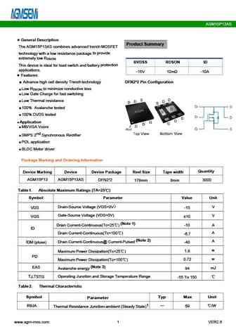
AGM15P13AS General Description Product Summary The AGM15P13AS combines advanced trench MOSFET to provide technology with a low resistance package extremely low R DS(ON) BVDSS RDSON ID protection This device is ideal for load switch and battery applications. -15V 12m -10A Features Advance high cell density Trench technology DFN2*2 Pin Configuration Low R to minimize ... See More ⇒
9.23. Size:1284K cn agmsemi
agm15t13c.pdf
AGM15T13C Table3. Electrical Characteristics (TJ=25 unless otherwise noted) Symbol Parameter Conditions Min Typ Max Unit On/Off States BV Drain-Source Breakdown Voltage V =0V I =250 A 150 -- V GS D DSS -- Zero Gate Voltage Drain Current V =150V,V =0V -- 1 A DS GS I -- DSS V = 20V,V =0V -- -- nA GS DS IGSS Gate-Body Leakage Current 100 V Gate Threshold Voltage V =V ... See More ⇒
Detailed specifications: AGM1405F, AGM14N10A, AGM14N10AP, AGM14N10D, AGM150P10AP, AGM150P10D, AGM150P10S, AGM15N10AP, 8205A, AGM305A, AGM305AP, AGM305D, AGM305MA, AGM306A, AGM306AP, AGM306C, AGM306D
Keywords - AGM15N10D MOSFET specs
AGM15N10D cross reference
AGM15N10D equivalent finder
AGM15N10D pdf lookup
AGM15N10D substitution
AGM15N10D replacement
Can't find your MOSFET?
Learn how to find a substitute transistor by analyzing voltage, current and package compatibility
