2SK660 Specs and Replacement
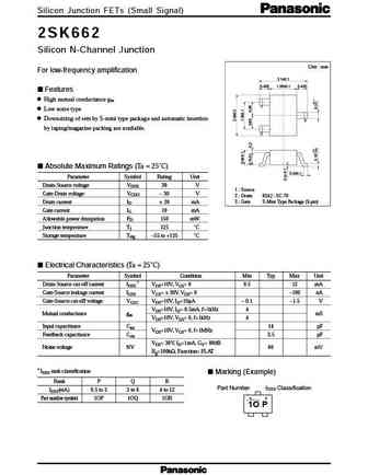
Type Designator: 2SK660
Type of Transistor: JFET
Type of Control Channel: N-Channel
Absolute Maximum Ratings
Pd ⓘ - Maximum Power Dissipation: 0.1 W
|Vds|ⓘ - Maximum Drain-Source Voltage: 20 V
|Id| ⓘ - Maximum Drain Current: 0.01 A
Tj ⓘ - Maximum Junction Temperature: 150 °C
Electrical Characteristics
Cossⓘ - Output Capacitance: 1.5 pF
RDSonⓘ - Maximum Drain-Source On-State Resistance: 1000 Ohm
Package: SST
2SK660 substitution
- MOSFET ⓘ Cross-Reference Search
2SK660 datasheet
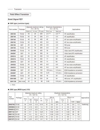
2sk104 2sk105 2sk162 2sk163 2sk193 2sk195 2sk505 2sk507 2sk514 2sk518 2sk519 2sk523 2sk533 2sk660 2sk997 2sk998 2sk1000 2sk1109.pdf
... See More ⇒
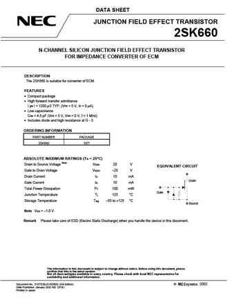
2sk660.pdf
DATA SHEET JUNCTION FIELD EFFECT TRANSISTOR 2SK660 N-CHANNEL SILICON JUNCTION FIELD EFFECT TRANSISTOR FOR IMPEDANCE CONVERTER OF ECM DESCRIPTION The 2SK660 is suitable for converter of ECM. FEATURES Compact package High forward transfer admittance yfs = 1200 S TYP. (VDS = 5 V, ID = 0 A) Low capacitance Ciss = 4.5 pF (VDS = 5 V, VGS = 0 V, f = 1 MHz) Include... See More ⇒
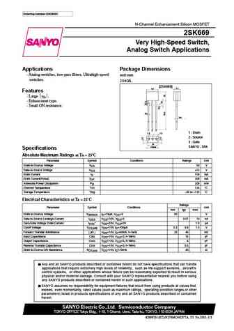
2sk669.pdf
Ordering number EN2563C N-Channel Enhancement Silicon MOSFET 2SK669 Very High-Speed Switch, Analog Switch Applications Applications Package Dimensions Analog switches, low-pass filters, Ultrahigh-speed unit mm switches. 2040A [2SK669] 2.2 4.0 Features Large yfs . Enhancemet type. 0.4 0.5 Small ON resistance. 0.4 0.4 1 2 3 1 Drain 1.3 1.3 2 Sour... See More ⇒
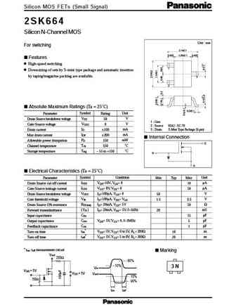
2sk664.pdf
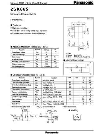
Silicon MOS FETs (Small Signal) 2SK664 2SK664 Silicon N-Channel MOS Unit mm For switching 2.1 0.1 0.425 1.25 0.1 0.425 Features High-speed switching 1 Downsizing of sets by S-mini type package and automatic insertion by taping/magazine packing are available. 3 2 Absolute Maximum Ratings (Ta = 25 C) 0.2 0.1 Symbol Parameter Rating Unit VDS Drain-Source breakdown v... See More ⇒
Detailed specifications: 2SK514, 2SK518, 2SK519, 2SK523, 2SK533, 2SK611, 2SK612, 2SK654, IRF9540N, 2SK679A, 2SK680A, 2SK681A, 2SK699, 2SK700, 2SK701, 2SK702, 2SK703
Keywords - 2SK660 MOSFET specs
2SK660 cross reference
2SK660 equivalent finder
2SK660 pdf lookup
2SK660 substitution
2SK660 replacement
Need a MOSFET replacement? Our guide shows you how to find a perfect substitute by comparing key parameters and specs
History: SP8K31FRA | IRFBC40LCPBF | DMP2002UPS-13 | RSH070P05TB1 | WMM90N08TS
🌐 : EN ES РУ
LIST
Last Update
MOSFET: FTF30P35D | FTF25N35DHVT | FTF15N35D | FTE15C35G | FTP02P15G | FTE02P15G | AKF30N5P0SX | AKF30N10S | AKF20P45D | CM4407
Popular searches
2sc632a | c3856 | 30100 transistor | 2sc1675 | k117 transistor | 2sc2291 | bc139 | 2sc1398
