DMC3021LK4 Specs and Replacement
Type Designator: DMC3021LK4
Type of Transistor: MOSFET
Type of Control Channel: NP-Channel
Absolute Maximum Ratings
Pd ⓘ - Maximum Power Dissipation: 2.75 W
|Vds|ⓘ - Maximum Drain-Source Voltage: 30 V
|Vgs|ⓘ - Maximum Gate-Source Voltage: 20 V
|Id| ⓘ - Maximum Drain Current: 9.4 A
Electrical Characteristics
RDSonⓘ - Maximum Drain-Source On-State Resistance: 0.032 Ohm
DMC3021LK4 substitution
- MOSFET ⓘ Cross-Reference Search
DMC3021LK4 datasheet
dmc3021lk4.pdf
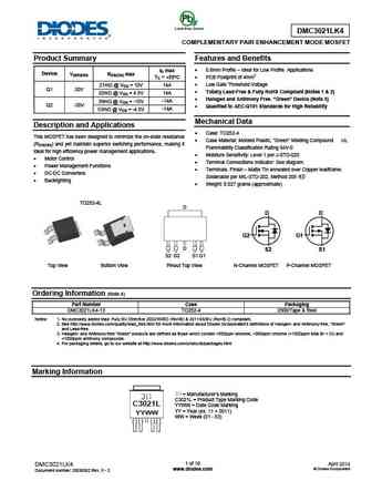
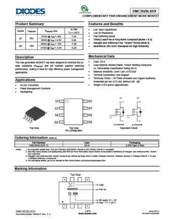
DMC3021LK4 COMPLEMENTARY PAIR ENHANCEMENT MODE MOSFET Product Summary Features and Benefits 0.6mm Profile Ideal for Low Profile Applications ID max Device V(BR)DSS RDS(ON) max TC = +25 C PCB Footprint of 4mm2 Low Gate Threshold Voltage 21m @ VGS = 10V 14A Q1 30V Totally Lead-Free & Fully RoHS Compliant (Notes 1 & 2) 32m @ VGS = 4.5V 14A Halog... See More ⇒
dmc3021lsd.pdf
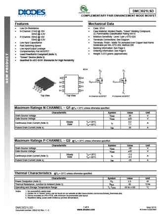
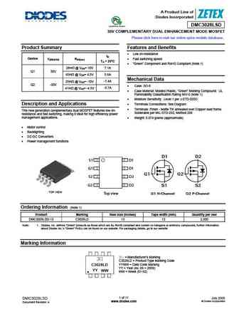
DMC3021LSD COMPLEMENTARY PAIR ENHANCEMENT MODE MOSFET Features Mechanical Data Low On-Resistance Case SO-8 N-Channel 21m @ 10V Case Material Molded Plastic, Green Molding Compound. UL Flammability Classification Rating 94V-0 32m @ 4.5V Moisture Sensitivity Level 1 per J-STD-020 P-Channel 39m @ 10V 53m @ 4.5V Terminals Connecti... See More ⇒
dmc3021lsdq.pdf
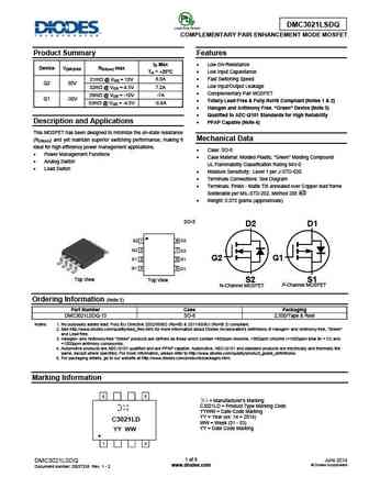
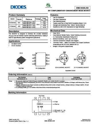
DMC3021LSDQ COMPLEMENTARY PAIR ENHANCEMENT MODE MOSFET Product Summary Features ID Max Low On-Resistance Device V(BR)DSS RDS(on) max TA = +25 C Low Input Capacitance Fast Switching Speed 21m @ VGS = 10V 8.5A Q2 30V Low Input/Output Leakage 32m @ VGS = 4.5V 7.2A Complementary Pair MOSFET 39m @ VGS = -10V -7A Q1 -30V Totally Lead-Free & Fully ... See More ⇒
fdmc3020dc.pdf
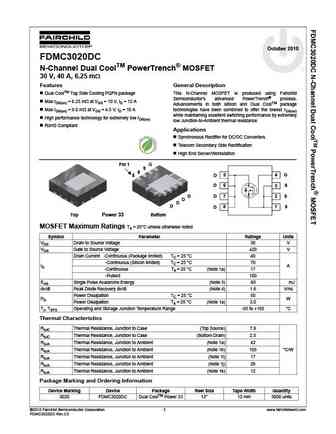
October 2010 FDMC3020DC N-Channel Dual CoolTM PowerTrench MOSFET 30 V, 40 A, 6.25 m Features General Description Dual CoolTM Top Side Cooling PQFN package This N-Channel MOSFET is produced using Fairchild Semiconductor s advanced PowerTrench process. Max rDS(on) = 6.25 m at VGS = 10 V, ID = 12 A Advancements in both silicon and Dual CoolTM package Max rDS(on) = 9.0 m a... See More ⇒
Detailed specifications: ZXMP2120G4, DMC2004DWK, DMC2004LPK, DMC2004VK, DMC2020USD, DMG1016UDW, DMG1016V, DMC3018LSD, 10N60, DMC3021LSD, DMC3028LSD, DMC3032LSD, DMC3036LSD, DMG6602SVT, ZXMC3A16DN8, ZXMC3A17DN8, ZXMC3A18DN8
Keywords - DMC3021LK4 MOSFET specs
DMC3021LK4 cross reference
DMC3021LK4 equivalent finder
DMC3021LK4 pdf lookup
DMC3021LK4 substitution
DMC3021LK4 replacement
Step-by-step guide to finding a MOSFET replacement. Cross-reference parts and ensure compatibility for your repair or project.
🌐 : EN ES РУ
LIST
Last Update
MOSFET: AUB062N08BG | AUB060N08AG | AUB056N10 | AUB056N08BGL | AUB050N085 | AUB050N055 | AUB045N12 | AUB045N10BT | AUB039N10 | AUB034N10
Popular searches
a1633 transistor | 2sa844 | 2sc1327 | 2sc3855 | 2sc945 transistor equivalent | 2sd427 | mje15032 equivalent | 2sc4834
