J310 Datasheet. Specs and Replacement
Type Designator: J310 📄📄
Type of Transistor: JFET
Type of Control Channel: N-Channel
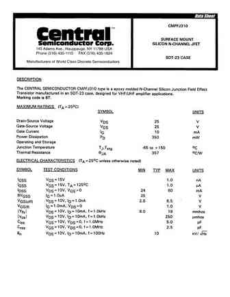
Absolute Maximum Ratings
Pd ⓘ - Maximum Power Dissipation: 0.4 W
|Vds|ⓘ - Maximum Drain-Source Voltage: 25 V
|Id| ⓘ - Maximum Drain Current: 0.05 A
Tj ⓘ - Maximum Junction Temperature: 150 °C
Electrical Characteristics
RDSonⓘ - Maximum Drain-Source On-State Resistance: 50 Ohm
Package: TO92
📄📄 Copy
J310 substitution
- MOSFET ⓘ Cross-Reference Search
J310 datasheet
j309 j310 mmbfj309 mmbfj310.pdf
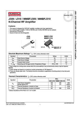
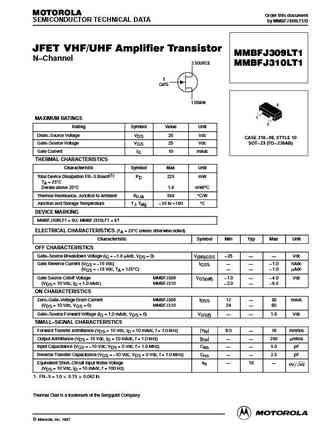
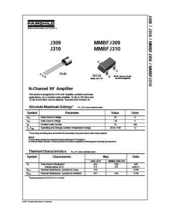
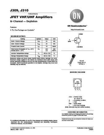
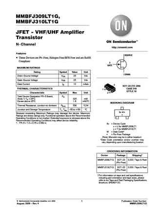
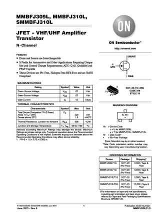
December 2010 J309 / J310 / MMBFJ309 / MMBFJ310 N-Channel RF Amplifier Features This device is designed for VHF/UHF amplifier, oscillator and mixer applications. As a common gate amplifier, 16 dB at 100 MHz and 12 dB at 450 MHz can be realized. Sourced from Process 92. Source & Drain are interchangeable. J309 MMBFJ309 J310 MMBFJ310 G S SOT-23 G TO-92 Mark MMBFJ309 ... See More ⇒
j310.pdf
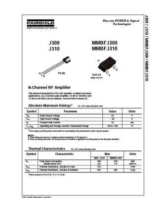
Discrete POWER & Signal Technologies J309 MMBFJ309 J310 MMBFJ310 G D G TO-92 S SOT-23 S D Mark 6U / 6T N-Channel RF Amplifier This device is designed for VHF/UHF amplifier, oscillator and mixer applications. As a common gate amplifier, 16 dB at 100 MHz and 12 dB at 450 MHz can be realized. Sourced from Process 92. Absolute Maximum Ratings* TA = 25 C unless otherwise noted Symbo... See More ⇒
j308 sst308 j309 sst309 j310 sst310 u309 u310.pdf
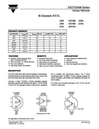
J/SST/U308 Series Vishay Siliconix N-Channel JFETs J308 SST308 U309 J309 SST309 U310 J310 SST310 PRODUCT SUMMARY Part Number VGS(off) (V) V(BR)GSS Min (V) gfs Min (mS) IDSS Min (mA) J308 -1 to -6.5 -25 8 12 J309 -1 to -4 -25 10 12 J310 -2 to -6.5 -25 8 24 SST308 -1 to -6.5 -25 8 12 SST309 -1 to -4 -25 10 12 SST310 -2 to -6.5 -25 8 24 U309 -1 to -4 -25 10 12 U310 -2.5 to -6 -25 10... See More ⇒
j308 j309 j310 sst308 sst310 sst309 u309 u310.pdf
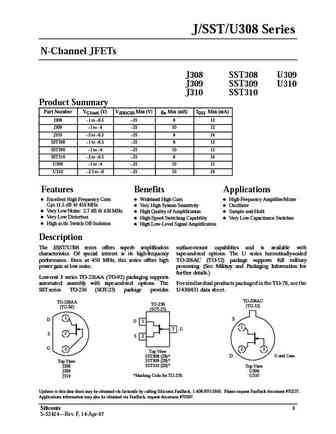
J/SST/U308 Series N-Channel JFETs J308 SST308 U309 J309 SST309 U310 J310 SST310 Product Summary Part Number VGS(off) (V) V(BR)GSS Min (V) gfs Min (mS) IDSS Min (mA) J308 1 to 6.5 25 8 12 J309 1 to 4 25 10 12 J310 2 to 6.5 25 8 24 SST308 1 to 6.5 25 8 12 SST309 1 to 4 25 10 12 SST310 2 to 6.5 25 8 24 U309 1 to 4 25 10 12... See More ⇒
Detailed specifications: FW274, FW282, FW707, FW811, FW812, FW813, FW906, FW907, IRFP250N, MCH3374, MCH3377, MCH3383, MCH3475, MCH3477, MCH3484, MCH6320, MCH6321
Keywords - J310 MOSFET specs
J310 cross reference
J310 equivalent finder
J310 pdf lookup
J310 substitution
J310 replacement
Can't find your MOSFET? Learn how to find a substitute transistor by analyzing voltage, current and package compatibility
🌐 : EN ES РУ

LIST
Last Update
MOSFET: MSH100N045SA | MSD60P16 | MSD40P45 | MSB100N023 | MS60P03 | MS40P05AU | MS40P05 | MS40N05 | MS34P07 | MS34P01
Popular searches
b772m transistor | mj15003g datasheet | irfp460n datasheet | mj15025g | ksa1381 replacement | m3056m mosfet | skd502t mosfet | tip 35 transistor