MTW32N20E Specs and Replacement
Type Designator: MTW32N20E
Type of Transistor: MOSFET
Type of Control Channel: N-Channel
Absolute Maximum Ratings
Pd ⓘ - Maximum Power Dissipation: 180 W
|Vds|ⓘ - Maximum Drain-Source Voltage: 200 V
|Vgs|ⓘ - Maximum Gate-Source Voltage: 20 V
|Id| ⓘ - Maximum Drain Current: 32 A
Tj ⓘ - Maximum Junction Temperature: 150 °C
Electrical Characteristics
tr ⓘ - Rise Time: 120 nS
Cossⓘ - Output Capacitance: 130 pF
RDSonⓘ - Maximum Drain-Source On-State Resistance: 0.075 Ohm
Package: TO247AE
MTW32N20E substitution
- MOSFET ⓘ Cross-Reference Search
MTW32N20E datasheet
mtw32n20e.pdf
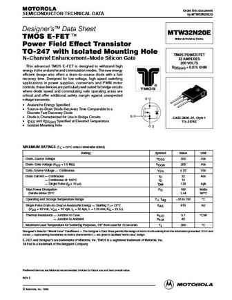
MOTOROLA Order this document SEMICONDUCTOR TECHNICAL DATA by MTW32N20E/D Designer's Data Sheet MTW32N20E TMOS E-FET. Motorola Preferred Device Power Field Effect Transistor TO-247 with Isolated Mounting Hole TMOS POWER FET N Channel Enhancement Mode Silicon Gate 32 AMPERES 200 VOLTS This advanced TMOS E FET is designed to withstand high RDS(on) = 0.075 OHM energy in t... See More ⇒
mtw32n20e.pdf
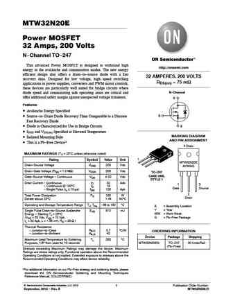
MTW32N20E Power MOSFET 32 Amps, 200 Volts N-Channel TO-247 This advanced Power MOSFET is designed to withstand high http //onsemi.com energy in the avalanche and commutation modes. The new energy efficient design also offers a drain-to-source diode with a fast 32 AMPERES, 200 VOLTS recovery time. Designed for low voltage, high speed switching RDS(on) = 75 mW applications in power sup... See More ⇒
mtw32n20e.pdf
INCHANGE Semiconductor isc N-Channel MOSFET Transistor MTW32N20E FEATURES With TO-247 packaging With low gate drive requirements Low switching loss Low on-state resistance Easy to drive 100% avalanche tested Minimum Lot-to-Lot variations for robust device performance and reliable operation APPLICATIONS Switching applications ABSOLUTE MAXIMUM RATINGS(T =25 ) ... See More ⇒
mtw32n20erev3.pdf
MOTOROLA Order this document SEMICONDUCTOR TECHNICAL DATA by MTW32N20E/D Designer's Data Sheet MTW32N20E TMOS E-FET. Motorola Preferred Device Power Field Effect Transistor TO-247 with Isolated Mounting Hole TMOS POWER FET N Channel Enhancement Mode Silicon Gate 32 AMPERES 200 VOLTS This advanced TMOS E FET is designed to withstand high RDS(on) = 0.075 OHM energy in t... See More ⇒
Detailed specifications: MTB2P50E , MTB50P03HDL , MTD5P06V , MTD6N15 , MTD6N20E , MTP20N15E , MTP2P50E , MTP50P03HDL , AO3400A , NCV8401 , NCV8402 , NCV8402D , NCV8403 , NCV8405 , NCV8406 , NCV8440 , NCV8450 .
Keywords - MTW32N20E MOSFET specs
MTW32N20E cross reference
MTW32N20E equivalent finder
MTW32N20E pdf lookup
MTW32N20E substitution
MTW32N20E replacement
Can't find your MOSFET? Learn how to find a substitute transistor by analyzing voltage, current and package compatibility
🌐 : EN ES РУ
LIST
Last Update
MOSFET: 2N7002KM | 2N7002KH | AON5802 | AOSS62934 | AOSN21319C | AONS66966 | AONR62992 | AON7400B | AON6578 | AO3480C
Popular searches
j5027-r datasheet | transistor a1015 datasheet | bf199 transistor equivalent | bu801 | c8550 transistor datasheet | mj21194 transistor datasheet | kep40n26 | nte103a


