NTJD4001N Specs and Replacement
Type Designator: NTJD4001N
Type of Transistor: MOSFET
Type of Control Channel: N-Channel
Absolute Maximum Ratings
Pd ⓘ - Maximum Power Dissipation: 0.272 W
|Vds|ⓘ - Maximum Drain-Source Voltage: 30 V
|Vgs|ⓘ - Maximum Gate-Source Voltage: 20 V
|Id| ⓘ - Maximum Drain Current: 0.25 A
Tj ⓘ - Maximum Junction Temperature: 150 °C
Electrical Characteristics
tr ⓘ - Rise Time: 23 nS
Cossⓘ - Output Capacitance: 19 pF
RDSonⓘ - Maximum Drain-Source On-State Resistance: 1.5 Ohm
NTJD4001N substitution
- MOSFET ⓘ Cross-Reference Search
NTJD4001N datasheet
ntjd4001n nvtjd4001n.pdf
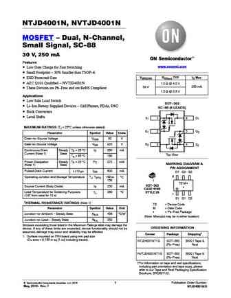
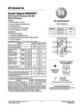
NTJD4001N, NVTJD4001N MOSFET Dual, N-Channel, Small Signal, SC-88 30 V, 250 mA Features www.onsemi.com Low Gate Charge for Fast Switching Small Footprint - 30% Smaller than TSOP-6 V(BR)DSS RDS(on) TYP ID Max ESD Protected Gate AEC Q101 Qualified - NVTJD4001N 1.0 W @ 4.0 V 250 mA 30 V These Devices are Pb-Free and are RoHS Compliant 1.5 W @ 2.5 V Applicatio... See More ⇒
ntjd4001n.pdf
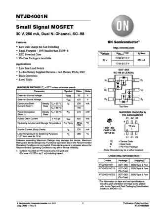
NTJD4001N Small Signal MOSFET 30 V, 250 mA, Dual N-Channel, SC-88 Features Low Gate Charge for Fast Switching http //onsemi.com Small Footprint - 30% Smaller than TSOP-6 V(BR)DSS RDS(on) TYP ID Max ESD Protected Gate 1.0 W @ 4.0 V Pb-Free Package is Available 250 mA 30 V 1.5 W @ 2.5 V Applications Low Side Load Switch SOT-363 Li-Ion Battery Supplied Devi... See More ⇒
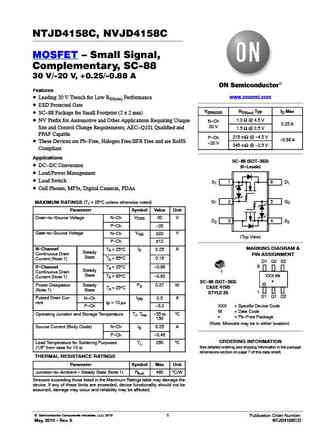
ntjd4158c.pdf
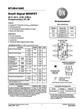
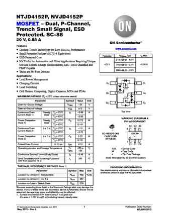
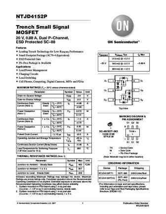
NTJD4158C Small Signal MOSFET 30 V/-20 V, +0.25/-0.88 A, Complementary, SC-88 Features http //onsemi.com Leading 20 V Trench for Low RDS(on) Performance ESD Protected Gate V(BR)DSS RDS(on) Typ ID Max SC-88 Package for Small Footprint (2 x 2 mm) 1.0 W @ 4.5 V N-Ch This is a Pb-Free Device 0.25 A 30 V 1.5 W @ 2.5 V Applications 215 mW @ -4.5 V P-Ch -0.88 A -20 V... See More ⇒
ntjd4105c.pdf
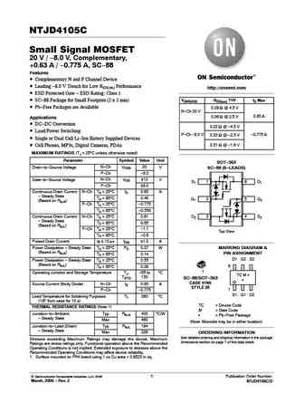
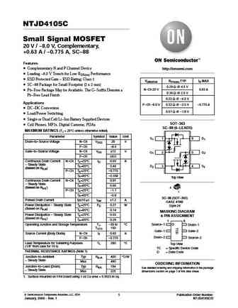
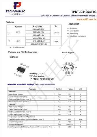
NTJD4105C Small Signal MOSFET 20 V / -8.0 V, Complementary, +0.63 A / -0.775 A, SC-88 Features Complementary N and P Channel Device Leading -8.0 V Trench for Low RDS(on) Performance http //onsemi.com ESD Protected Gate - ESD Rating Class 1 SC-88 Package for Small Footprint (2 x 2 mm) V(BR)DSS RDS(on) TYP ID Max Pb-Free Packages are Available 0.29 W @ 4.5 V N-Ch... See More ⇒

Detailed specifications: NTHD4508N, SRC60R090B, NTHS4101P, NTHS4166N, NTHS5404, NTHS5441T1, NTHS5443, NTJD1155L, STP75NF75, NTJD4105C, NTJD4152P, NTJD4158C, NTJD4401N, NTJD5121N, NTJS3151P, NTJS3157N, NTJS4151P
Keywords - NTJD4001N MOSFET specs
NTJD4001N cross reference
NTJD4001N equivalent finder
NTJD4001N pdf lookup
NTJD4001N substitution
NTJD4001N replacement
Step-by-step guide to finding a MOSFET replacement. Cross-reference parts and ensure compatibility for your repair or project.
History: WMLL020N10HG4 | SUM6K1N | SRC60R090B
🌐 : EN ES РУ

LIST
Last Update
MOSFET: AUB034N10 | AUB033N08BG | AUB026N085 | AUA062N08BG | AUA060N08AG | AUA056N08BGL | AUA039N10 | ASW80R290E | ASW65R120EFD | ASW65R110E
Popular searches
mpsa56 | c3205 transistor | tip35c datasheet | 2n5401 datasheet | mj21194g | irfz34n | mn2488 | irfb438