NTLJD3115P Specs and Replacement
Type Designator: NTLJD3115P
Type of Transistor: MOSFET
Type of Control Channel: P-Channel
Absolute Maximum Ratings
Pd ⓘ - Maximum Power Dissipation: 0.71 W
|Vds|ⓘ - Maximum Drain-Source Voltage: 20 V
|Vgs|ⓘ - Maximum Gate-Source Voltage: 8 V
|Id| ⓘ - Maximum Drain Current: 2.3 A
Tj ⓘ - Maximum Junction Temperature: 150 °C
Electrical Characteristics
tr ⓘ - Rise Time: 11 nS
Cossⓘ - Output Capacitance: 91 pF
Rds ⓘ - Maximum Drain-Source On-State Resistance: 0.1 Ohm
Package: WDFN6
NTLJD3115P substitution
- MOSFET ⓘ Cross-Reference Search
NTLJD3115P datasheet
ntljd3115p.pdf
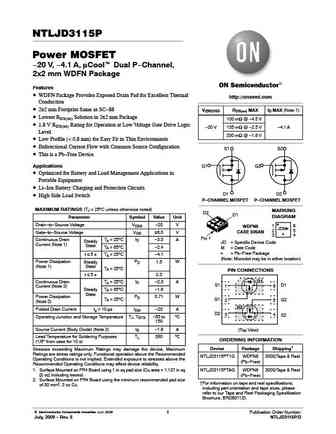
NTLJD3115P Power MOSFET -20 V, -4.1 A, mCoolt Dual P-Channel, 2x2 mm WDFN Package Features WDFN Package Provides Exposed Drain Pad for Excellent Thermal http //onsemi.com Conduction 2x2 mm Footprint Same as SC-88 V(BR)DSS RDS(on) MAX ID MAX (Note 1) Lowest RDS(on) Solution in 2x2 mm Package 100 mW @ -4.5 V 1.8 V RDS(on) Rating for Operation at Low Voltage Gate Drive ... See More ⇒
ntljd3182fztag ntljd3182fztbg.pdf
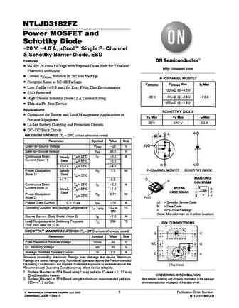
NTLJD3182FZ Power MOSFET and Schottky Diode -20 V, -4.0 A, mCoolt Single P-Channel & Schottky Barrier Diode, ESD Features WDFN 2x2 mm Package with Exposed Drain Pads for Excellent http //onsemi.com Thermal Conduction Lowest RDS(on) Solution in 2x2 mm Package P-CHANNEL MOSFET Footprint Same as SC-88 Package V(BR)DSS RDS(on) Max ID Max Low Profile (... See More ⇒
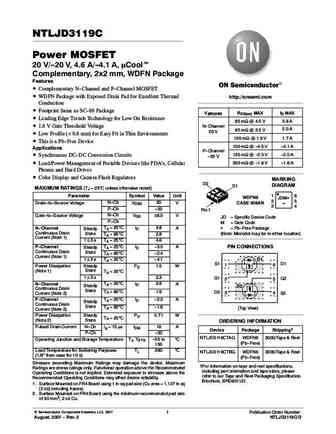
Detailed specifications: NTJS3157N , NTJS4151P , NTJS4405N , NTK3043N , NTK3134N , NTK3139P , NTLGD3502N , NTLGF3402P , 5N65 , NTLJD3119C , NTLJD4116N , NTLJF3117P , NTLJF4156N , NTLJS2103P , NTLJS3113P , NTLJS4114N , QM3098M6 .
Keywords - NTLJD3115P MOSFET specs
NTLJD3115P cross reference
NTLJD3115P equivalent finder
NTLJD3115P pdf lookup
NTLJD3115P substitution
NTLJD3115P replacement
Can't find your MOSFET? Learn how to find a substitute transistor by analyzing voltage, current and package compatibility
History: FXN30N50F | FXN2N60D


LIST
Last Update
MOSFET: AOT66613L | AOSP21313C | AOSP21311C | AOB66918L | AO3415C | AOTF20N40L | AOTF11N60L | AOT11N60L | AONS21303C | AOI280A60
Popular searches
2n3904 transistor datasheet | p75nf75 | d880 transistor | 2sc1845 | p60nf06 | 2sa1837 | ksc1845 transistor | irf630 datasheet