View j111 j112 j113 cnv detailed specification:
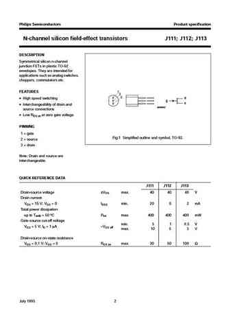
DISCRETE SEMICONDUCTORS DATA SHEET J111; J112; J113 N-channel silicon field-effect transistors July 1993 Product specification File under Discrete Semiconductors, SC07 Philips Semiconductors Product specification N-channel silicon field-effect transistors J111; J112; J113 DESCRIPTION Symmetrical silicon n-channel junction FETs in plastic TO-92 envelopes. They are intended for applications such as analog switches, choppers, commutators etc. FEATURES 1 handbook, halfpage 2 3 d High speed switching g s Interchangeability of drain and MAM042 source connections Low RDS on at zero gate voltage PINNING 1 = gate Fig.1 Simplified outline and symbol, TO-92. 2 = source 3 = drain Note Drain and source are interchangeable. QUICK REFERENCE DATA J111 J112 J113 Drain-source voltage VDS max. 40 40 40 V Drain current VDS = 15 V; VGS =0 IDSS min. 20... See More ⇒
Keywords - ALL TRANSISTORS SPECS
j111 j112 j113 cnv.pdf Design, MOSFET, Power
j111 j112 j113 cnv.pdf RoHS Compliant, Service, Triacs, Semiconductor
j111 j112 j113 cnv.pdf Database, Innovation, IC, Electricity
BJT Parameters and How They Relate
🌐 : EN ES РУ

LIST
Last Update
BJT: ZDT6705 | GA1L4Z | GA1A4M | SBT42 | 2SA200-Y | 2SA200-O
Popular searches
irfz44n | irf3205 | irfz44n datasheet | 2n4401 | bc547 transistor | bd139 | 2n4401 datasheet