Скачать даташит для hgtg20n120:

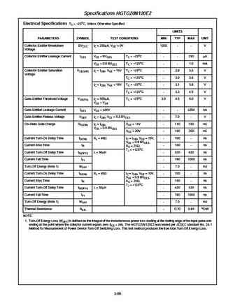
S E M I C O N D U C T O R HGTG20N120E2 34A, 1200V N-Channel IGBT April 1995 Features Package JEDEC STYLE TO-247 34A, 1200V Latch Free Operation EMITTER Typical Fall Time - 780ns COLLECTOR GATE High Input Impedance COLLECTOR Low Conduction Loss (BOTTOM SIDE METAL) Description The HGTG20N120E2 is a MOS gated, high voltage switch- ing device combining the best features of MOSFETs and bipolar transistors. The device has the high input impedance of a MOSFET and the low on-state conduction loss of a bipolar transistor. The much lower on-state voltage drop Terminal Diagram varies only moderately between +25oC and +150oC. IGBTs are ideal for many high voltage switching applications C operating at frequencies where low conduction losses are essential, such as AC and DC motor controls, power supplies and drivers for solenoids, relays and contactors
Ключевые слова - ALL TRANSISTORS DATASHEET
hgtg20n120.pdf Проектирование, MOSFET, Мощность
hgtg20n120.pdf Соответствует RoHS, Сервис, Симисторы, Полупроводник
hgtg20n120.pdf База данных, Инновации, ИМС, Транзисторы
Параметры биполярного транзистора и их взаимосвязь

Список транзисторов
Обновления
BJT: ZDT6705 | GA1L4Z | GA1A4M | SBT42 | 2SA200-Y | 2SA200-O | 2SD882-Q | 2SD882-P | 2SD882-E | 2SC945-L | 2SC945-H | 2SC4226-R23 | 2SC3357-F | 2SC3357-E | 2SC3356-R26 | 2SC3356-R24 | 2SC3356-R23 | 2SB772-Q | 2SB772-P | 2SB772-E | 2SA1015-L
Popular searches
irfz44n | irf3205 | irfz44n datasheet | 2n4401 | bc547 transistor | bd139 | 2n4401 datasheet