APT30M90AVR. Аналоги и основные параметры
Наименование производителя: APT30M90AVR
Тип транзистора: MOSFET
Полярность: N
Предельные значения
Pd ⓘ - Максимальная рассеиваемая мощность: 235 W
|Vds|ⓘ - Максимально допустимое напряжение сток-исток: 300 V
|Vgs|ⓘ - Максимально допустимое напряжение затвор-исток: 30 V
|Id| ⓘ - Максимально допустимый постоянный ток стока: 33 A
Tj ⓘ - Максимальная температура канала: 150 °C
Электрические характеристики
tr ⓘ - Время нарастания: 10 ns
Cossⓘ - Выходная емкость: 700 pf
RDSonⓘ - Сопротивление сток-исток открытого транзистора: 0.09 Ohm
Тип корпуса: TO3
Аналог (замена) для APT30M90AVR
- подборⓘ MOSFET транзистора по параметрам
APT30M90AVR даташит
apt30m90avr.pdf
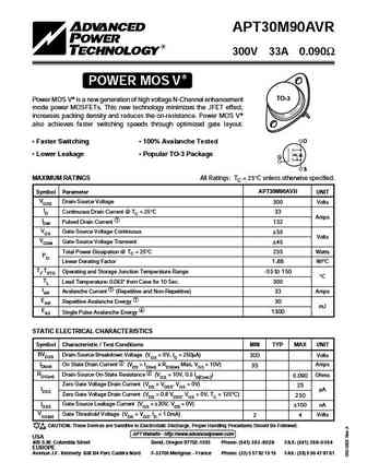
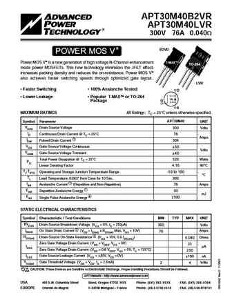
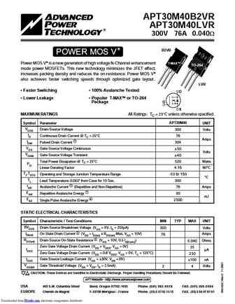
APT30M90AVR 300V 33A 0.090 POWER MOS V TO-3 Power MOS V is a new generation of high voltage N-Channel enhancement mode power MOSFETs. This new technology minimizes the JFET effect, increases packing density and reduces the on-resistance. Power MOS V also achieves faster switching speeds through optimized gate layout. D Faster Switching 100% Avalanche Tested Lower
apt30m40b2vfrg.pdf
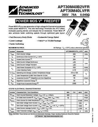
APT30M40B2VFR APT30M40LVFR 300V 76A 0.040 B2VFR POWER MOS V FREDFET T-MAX TO-264 Power MOS V is a new generation of high voltage N-Channel enhancement mode power MOSFETs. This new technology minimizes the JFET effect, increases packing density and reduces the on-resistance. Power MOS V also achieves faster switching speeds through optimized gate layout
apt30m85.pdf

APT30M85BVFR 300V 40A 0.085 POWER MOS V FREDFET Power MOS V is a new generation of high voltage N-Channel enhancement TO-247 mode power MOSFETs. This new technology minimizes the JFET effect, increases packing density and reduces the on-resistance. Power MOS V also achieves faster switching speeds through optimized gate layout. Fast Recovery Body Diode 100% Avalanche Tes
apt30m75bll.pdf

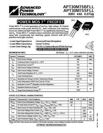
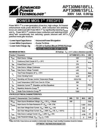
APT30M75BLL APT30M75SLL 300V 44A 0.075W TM BLL POWER MOS 7 Power MOS 7TM is a new generation of low loss, high voltage, N-Channel D3PAK TO-247 enhancement mode power MOSFETS. Both conduction and switching losses are addressed with Power MOS 7TM by significantly lowering RDS(ON) and Qg. Power MOS 7TM combines lower conduction and switching losses along with exceptionally fast switchin
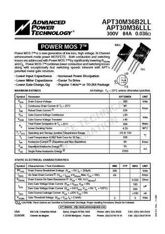
apt30m36b2fll apt30m36lfll.pdf
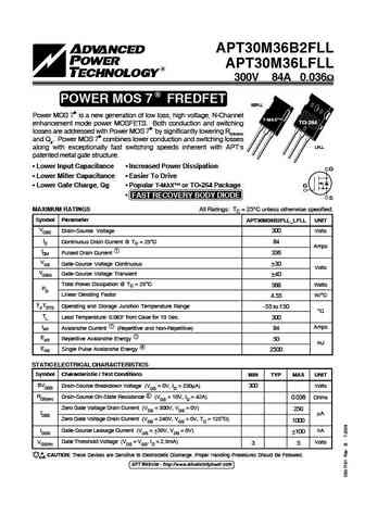
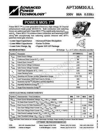
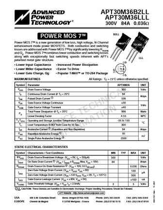
APT30M36B2FLL APT30M36LFLL 300V 84A 0.036 R FREDFET POWER MOS 7 FREDFET B2FLL Power MOS 7 is a new generation of low loss, high voltage, N-Channel T-MAX TO-264 enhancement mode power MOSFETS. Both conduction and switching losses are addressed with Power MOS 7 by significantly lowering RDS(ON) and Qg. Power MOS 7 combines lower conduction and switchin
apt30m17jll.pdf
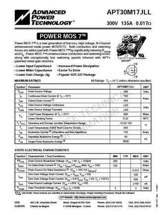
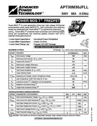
APT30M17JLL 300V 135A 0.017W TM POWER MOS 7 Power MOS 7TM is a new generation of low loss, high voltage, N-Channel enhancement mode power MOSFETS. Both conduction and switching losses are addressed with Power MOS 7TM by significantly lowering RDS(ON) and Qg. Power MOS 7TM combines lower conduction and switching losses along with exceptionally fast switching speeds inherent with APT's
apt30m75bfllg apt30m75sfllg.pdf
APT30M75BFLL APT30M75SFLL 300V 44A 0.075 BFLL R POWER MOS 7 FREDFET D3PAK Power MOS 7 is a new generation of low loss, high voltage, N-Channel TO-247 enhancement mode power MOSFETS. Both conduction and switching losses are addressed with Power MOS 7 by significantly lowering RDS(ON) and Qg. Power MOS 7 combines lower conduction and switching losses SFLL
apt30m85svrg.pdf
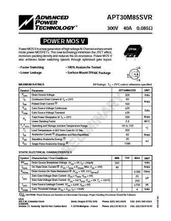
APT30M85SVR 300V 40A 0.085 POWER MOS V Power MOS V is a new generation of high voltage N-Channel enhancement D3PAK mode power MOSFETs. This new technology minimizes the JFET effect, increases packing density and reduces the on-resistance. Power MOS V also achieves faster switching speeds through optimized gate layout. Faster Switching 100% Avalanche Tested D Lower Lea
apt30m19jvfr.pdf
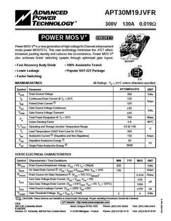
APT30M19JVFR 300V 130A 0.019 POWER MOS V FREDFET Power MOS V is a new generation of high voltage N-Channel enhancement mode power MOSFETs. This new technology minimizes the JFET effect, increases packing density and reduces the on-resistance. Power MOS V also achieves faster switching speeds through optimized gate layout. ISOTOP Fast Recovery Body Diode 100% Avalanche
apt30m36jfll.pdf
APT30M36JFLL 300V 76A 0.036 R POWER MOS 7 FREDFET Power MOS 7 is a new generation of low loss, high voltage, N-Channel enhancement mode power MOSFETS. Both conduction and switching losses are addressed with Power MOS 7 by significantly lowering RDS(ON) "UL Recognized" and Qg. Power MOS 7 combines lower conduction and switching losses ISOTOP along with e
apt30m40b2vr.pdf
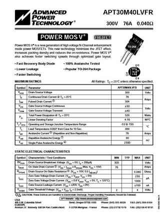
APT30M40B2VR APT30M40LVR 300V 76A 0.040W B2VR POWER MOS V T-MAX Power MOS V is a new generation of high voltage N-Channel enhancement TO-264 mode power MOSFETs. This new technology minimizes the JFET effect, increases packing density and reduces the on-resistance. Power MOS V also achieves faster switching speeds through optimized gate layout.. LVR Faster Switching
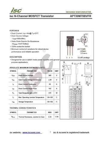
apt30m70bvr.pdf
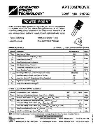
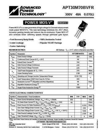
APT30M70BVR 300V 48A 0.070 POWER MOS V Power MOS V is a new generation of high voltage N-Channel enhancement TO-247 mode power MOSFETs. This new technology minimizes the JFET effect, increases packing density and reduces the on-resistance. Power MOS V also achieves faster switching speeds through optimized gate layout. D Faster Switching 100% Avalanche Tested Lower
apt30m75bllg apt30m75sllg.pdf
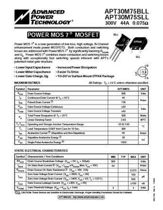
APT30M75BLL APT30M75SLL 300V 44A 0.075 R BLL POWER MOS 7 MOSFET D3PAK Power MOS 7 is a new generation of low loss, high voltage, N-Channel TO-247 enhancement mode power MOSFETS. Both conduction and switching losses are addressed with Power MOS 7 by significantly lowering RDS(ON) and Qg. Power MOS 7 combines lower conduction and switching losses SLL alo
apt30m30b2llg apt30m30lllg.pdf
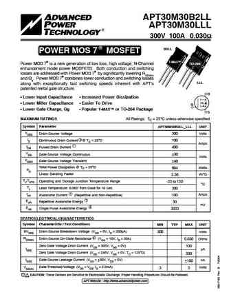
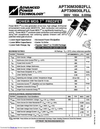
APT30M30B2LL APT30M30LLL 300V 100A 0.030 R B2LL POWER MOS 7 MOSFET T-MAX Power MOS 7 is a new generation of low loss, high voltage, N-Channel TO-264 enhancement mode power MOSFETS. Both conduction and switching losses are addressed with Power MOS 7 by significantly lowering RDS(ON) and Qg. Power MOS 7 combines lower conduction and switching losses LLL
apt30m36jll.pdf
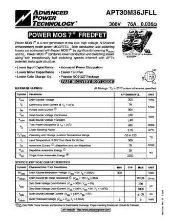
APT30M36JLL 300V 76A 0.036W TM POWER MOS 7 Power MOS 7TM is a new generation of low loss, high voltage, N-Channel enhancement mode power MOSFETS. Both conduction and switching losses are addressed with Power MOS 7TM by significantly lowering RDS(ON) and Qg. Power MOS 7TM combines lower conduction and switching losses along with exceptionally fast switching speeds inherent with APT's "
apt30m61bll.pdf

APT30M61BLL APT30M61SLL 300V 54A 0.061W TM BLL POWER MOS 7 Power MOS 7TM is a new generation of low loss, high voltage, N-Channel D3PAK TO-247 enhancement mode power MOSFETS. Both conduction and switching losses are addressed with Power MOS 7TM by significantly lowering RDS(ON) and Qg. Power MOS 7TM combines lower conduction and switching losses along with exceptionally fast switchin
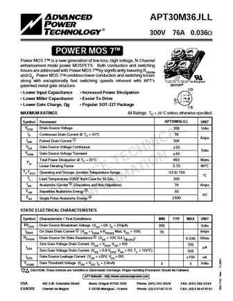
apt30m85bvfr.pdf
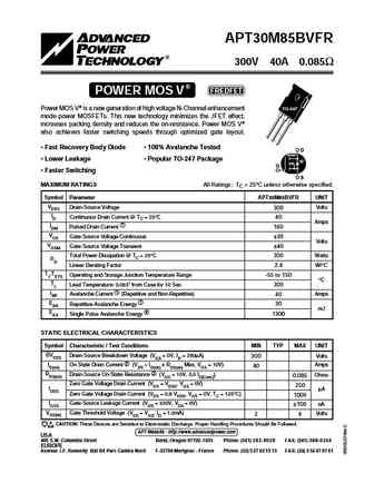
APT30M85BVFR 300V 40A 0.085 POWER MOS V FREDFET Power MOS V is a new generation of high voltage N-Channel enhancement TO-247 mode power MOSFETs. This new technology minimizes the JFET effect, increases packing density and reduces the on-resistance. Power MOS V also achieves faster switching speeds through optimized gate layout. Fast Recovery Body Diode 100% Avalanche Tes
apt30m85bvr.pdf
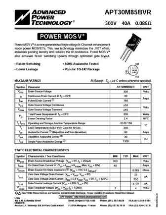
APT30M85BVR 300V 40A 0.085 POWER MOS V Power MOS V is a new generation of high voltage N-Channel enhancement TO-247 mode power MOSFETs. This new technology minimizes the JFET effect, increases packing density and reduces the on-resistance. Power MOS V also achieves faster switching speeds through optimized gate layout. Faster Switching 100% Avalanche Tested D Lower
apt30m36lll apt30m36b2ll.pdf
APT30M36B2LL APT30M36LLL 300V 84A 0.036W B2LL TM POWER MOS 7 Power MOS 7TM is a new generation of low loss, high voltage, N-Channel T-MAX TO-264 enhancement mode power MOSFETS. Both conduction and switching losses are addressed with Power MOS 7TM by significantly lowering RDS(ON) and Qg. Power MOS 7TM combines lower conduction and switching losses along with exceptionally fast s
apt30m40jvr.pdf

APT30M40JVR 300V 70A 0.040 POWER MOS V Power MOS V is a new generation of high voltage N-Channel enhancement mode power MOSFETs. This new technology minimizes the JFET effect, increases packing density and reduces the on-resistance. Power MOS V also achieves faster switching speeds through optimized gate layout. "UL Recognized" ISOTOP D Faster Switching 100% Avalanc
apt30m30jll.pdf
APT30M30JLL 300V 88A 0.030W TM POWER MOS 7 Power MOS 7TM is a new generation of low loss, high voltage, N-Channel enhancement mode power MOSFETS. Both conduction and switching losses are addressed with Power MOS 7TM by significantly lowering RDS(ON) and Qg. Power MOS 7TM combines lower conduction and switching losses along with exceptionally fast switching speeds inherent with APT's "
apt30m36b2ll.pdf
APT30M36B2LL APT30M36LLL 300V 84A 0.036W B2LL TM POWER MOS 7 Power MOS 7TM is a new generation of low loss, high voltage, N-Channel T-MAX TO-264 enhancement mode power MOSFETS. Both conduction and switching losses are addressed with Power MOS 7TM by significantly lowering RDS(ON) and Qg. Power MOS 7TM combines lower conduction and switching losses along with exceptionally fast s
apt30m70bvfr.pdf
APT30M70BVFR 300V 48A 0.070 POWER MOS V FREDFET Power MOS V is a new generation of high voltage N-Channel enhancement TO-247 mode power MOSFETs. This new technology minimizes the JFET effect, increases packing density and reduces the on-resistance. Power MOS V also achieves faster switching speeds through optimized gate layout. Fast Recovery Body Diode 100% Avalanche Tes
apt30m30b2ll.pdf

APT30M30B2LL APT30M30LLL 300V 100A 0.030W B2LL TM POWER MOS 7 Power MOS 7TM is a new generation of low loss, high voltage, N-Channel T-MAX TO-264 enhancement mode power MOSFETS. Both conduction and switching losses are addressed with Power MOS 7TM by significantly lowering RDS(ON) and Qg. Power MOS 7TM combines lower conduction and switching losses along with exceptionally fast
apt30m30jfll.pdf
APT30M30JFLL 300V 88A 0.030 R POWER MOS 7 FREDFET Power MOS 7 is a new generation of low loss, high voltage, N-Channel enhancement mode power MOSFETS. Both conduction and switching losses are addressed with Power MOS 7 by significantly lowering RDS(ON) and Qg. Power MOS 7 combines lower conduction and switching losses along with exceptionally fast switching
apt30m40b2vrg.pdf
APT30M40B2VR APT30M40LVR 300V 76A 0.040W B2VR POWER MOS V T-MAX Power MOS V is a new generation of high voltage N-Channel enhancement TO-264 mode power MOSFETs. This new technology minimizes the JFET effect, increases packing density and reduces the on-resistance. Power MOS V also achieves faster switching speeds through optimized gate layout.. LVR Faster Switching
apt30m40lvfr.pdf
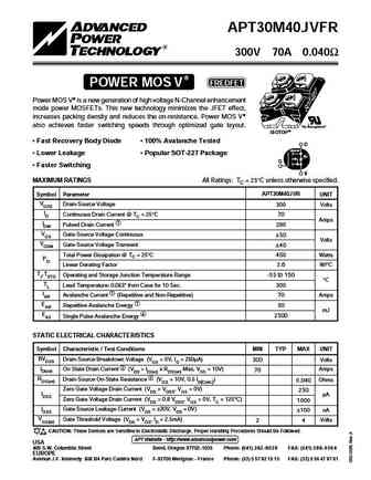
APT30M40LVFR 300V 76A 0.040 POWER MOS V FREDFET Power MOS V is a new generation of high voltage N-Channel enhancement TO-264 mode power MOSFETs. This new technology minimizes the JFET effect, increases packing density and reduces the on-resistance. Power MOS V also achieves faster switching speeds through optimized gate layout. Fast Recovery Body Diode 100% Avalanche Te
apt30m30b2fllg apt30m30lfll.pdf
APT30M30B2FLL APT30M30LFLL 300V 100A 0.030 R B2FLL POWER MOS 7 FREDFET T-MAX Power MOS 7 is a new generation of low loss, high voltage, N-Channel TO-264 enhancement mode power MOSFETS. Both conduction and switching losses are addressed with Power MOS 7 by significantly lowering RDS(ON) and Qg. Power MOS 7 combines lower conduction and switching losses
apt30m61bfllg apt30m61sfllg.pdf
APT30M61BFLL APT30M61SFLL 300V 54A 0.061 R POWER MOS 7 FREDFET D3PAK Power MOS 7 is a new generation of low loss, high voltage, N-Channel TO-247 enhancement mode power MOSFETS. Both conduction and switching losses are addressed with Power MOS 7 by significantly lowering RDS(ON) and Qg. Power MOS 7 combines lower conduction and switching losses along with
apt30m19jvr.pdf
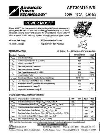
APT30M19JVR 300V 130A 0.019 POWER MOS V Power MOS V is a new generation of high voltage N-Channel enhancement mode power MOSFETs. This new technology minimizes the JFET effect, increases packing density and reduces the on-resistance. Power MOS V also achieves faster switching speeds through optimized gate layout. "UL Recognized" ISOTOP Faster Switching 100% Avalanche
apt30m17jfll.pdf
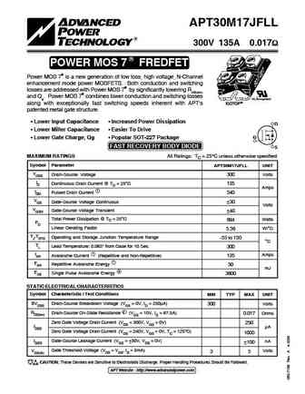
APT30M17JFLL 300V 135A 0.017 R POWER MOS 7 FREDFET Power MOS 7 is a new generation of low loss, high voltage, N-Channel enhancement mode power MOSFETS. Both conduction and switching losses are addressed with Power MOS 7 by significantly lowering RDS(ON) and Qg. Power MOS 7 combines lower conduction and switching losses "UL Recognized" along with exceptiona
apt30m60j.pdf
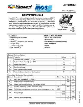
APT30M60J 600V, 31A, 0.15 Max N-Channel MOSFET Power MOS 8 is a high speed, high voltage N-channel switch-mode power MOSFET. A proprietary planar stripe design yields excellent reliability and manufacturability. Low switching loss is achieved with low input capacitance and ultra low Crss "Miller" capaci- tance. The intrinsic gate resistance and capacitance of the poly-silicon ga
apt30m36b2fll.pdf

isc N-Channel MOSFET Transistor APT30M36B2FLL FEATURES Drain Current I = 84A@ T =25 D C Drain Source Voltage- V =300V(Min) DSS Static Drain-Source On-Resistance R =0.036 (Max) DS(on) 100% avalanche tested Minimum Lot-to-Lot variations for robust device performance and reliable operation DESCRIPTION Designed for use in switch mode power supplies and general
apt30m75bll.pdf
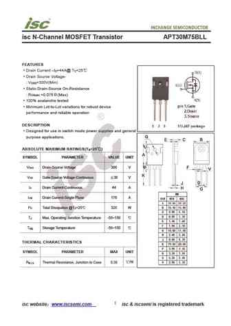
isc N-Channel MOSFET Transistor APT30M75BLL FEATURES Drain Current I =44A@ T =25 D C Drain Source Voltage- V =300V(Min) DSS Static Drain-Source On-Resistance R =0.075 (Max) DS(on) 100% avalanche tested Minimum Lot-to-Lot variations for robust device performance and reliable operation DESCRIPTION Designed for use in switch mode power supplies and general pur
apt30m36lll.pdf
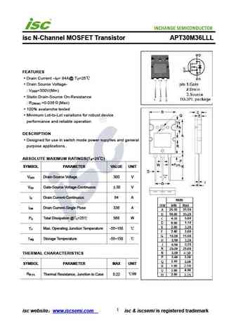
isc N-Channel MOSFET Transistor APT30M36LLL FEATURES Drain Current I = 84A@ T =25 D C Drain Source Voltage- V =300V(Min) DSS Static Drain-Source On-Resistance R =0.036 (Max) DS(on) 100% avalanche tested Minimum Lot-to-Lot variations for robust device performance and reliable operation DESCRIPTION Designed for use in switch mode power supplies and general pu
apt30m75bfll.pdf

isc N-Channel MOSFET Transistor APT30M75BFLL FEATURES Drain Current I = 44A@ T =25 D C Drain Source Voltage- V =300V(Min) DSS Static Drain-Source On-Resistance R =0.075 (Max) DS(on) 100% avalanche tested Minimum Lot-to-Lot variations for robust device performance and reliable operation DESCRIPTION Designed for use in switch mode power supplies and general p
apt30m70bvr.pdf

isc N-Channel MOSFET Transistor APT30M70BVR FEATURES Drain Current I =48A@ T =25 D C Drain Source Voltage- V =300V(Min) DSS Static Drain-Source On-Resistance R =0.07 (Max) DS(on) 100% avalanche tested Minimum Lot-to-Lot variations for robust device performance and reliable operation DESCRIPTION Designed for use in switch mode power supplies and general purp
apt30m30b2fll.pdf

isc N-Channel MOSFET Transistor APT30M30B2FLL FEATURES Drain Current I = 100A@ T =25 D C Drain Source Voltage- V =300V(Min) DSS Static Drain-Source On-Resistance R =0.03 (Max) DS(on) 100% avalanche tested Minimum Lot-to-Lot variations for robust device performance and reliable operation DESCRIPTION Designed for use in switch mode power supplies and general
apt30m36lfll.pdf

isc N-Channel MOSFET Transistor APT30M36LFLL FEATURES Drain Current I = 100A@ T =25 D C Drain Source Voltage- V =300V(Min) DSS Static Drain-Source On-Resistance R =0.03 (Max) DS(on) 100% avalanche tested Minimum Lot-to-Lot variations for robust device performance and reliable operation DESCRIPTION Designed for use in switch mode power supplies and general p
apt30m30lfll.pdf

isc N-Channel MOSFET Transistor APT30M30LFLL FEATURES Drain Current I = 100A@ T =25 D C Drain Source Voltage- V =300V(Min) DSS Static Drain-Source On-Resistance R =0.03 (Max) DS(on) 100% avalanche tested Minimum Lot-to-Lot variations for robust device performance and reliable operation DESCRIPTION Designed for use in switch mode power supplies and general p
apt30m61bll.pdf

isc N-Channel MOSFET Transistor APT30M61BLL FEATURES Drain Current I =54A@ T =25 D C Drain Source Voltage- V =300V(Min) DSS Static Drain-Source On-Resistance R =0.061 (Max) DS(on) 100% avalanche tested Minimum Lot-to-Lot variations for robust device performance and reliable operation DESCRIPTION Designed for use in switch mode power supplies and general pur
apt30m61bfll.pdf

isc N-Channel MOSFET Transistor APT30M61BFLL FEATURES Drain Current I = 54A@ T =25 D C Drain Source Voltage- V =300V(Min) DSS Static Drain-Source On-Resistance R =0.061 (Max) DS(on) 100% avalanche tested Minimum Lot-to-Lot variations for robust device performance and reliable operation DESCRIPTION Designed for use in switch mode power supplies and general p
apt30m85bvr.pdf

isc N-Channel MOSFET Transistor APT30M85BVR FEATURES Drain Current I =40A@ T =25 D C Drain Source Voltage- V =300V(Min) DSS Static Drain-Source On-Resistance R =0.085 (Max) DS(on) 100% avalanche tested Minimum Lot-to-Lot variations for robust device performance and reliable operation DESCRIPTION Designed for use in switch mode power supplies and general pur
apt30m36b2ll.pdf

isc N-Channel MOSFET Transistor APT30M36B2LL FEATURES Drain Current I = 84A@ T =25 D C Drain Source Voltage- V =300V(Min) DSS Static Drain-Source On-Resistance R =0.036 (Max) DS(on) 100% avalanche tested Minimum Lot-to-Lot variations for robust device performance and reliable operation DESCRIPTION Designed for use in switch mode power supplies and general p
apt30m70bvfr.pdf
isc N-Channel MOSFET Transistor APT30M70BVFR FEATURES Drain Current I = 48A@ T =25 D C Drain Source Voltage- V =300V(Min) DSS Static Drain-Source On-Resistance R =0.07 (Max) DS(on) 100% avalanche tested Minimum Lot-to-Lot variations for robust device performance and reliable operation DESCRIPTION Designed for use in switch mode power supplies and general pu
apt30m30b2ll.pdf
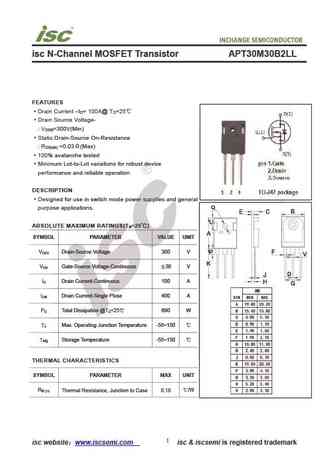
isc N-Channel MOSFET Transistor APT30M30B2LL FEATURES Drain Current I = 100A@ T =25 D C Drain Source Voltage- V =300V(Min) DSS Static Drain-Source On-Resistance R =0.03 (Max) DS(on) 100% avalanche tested Minimum Lot-to-Lot variations for robust device performance and reliable operation DESCRIPTION Designed for use in switch mode power supplies and general p
Другие IGBT... APT30M40JVFR, APT30M40JVR, APT30M40LVFR, APT30M40LVR, APT30M70BVFR, APT30M70BVR, APT30M85BVFR, APT30M85BVR, IRFP260N, APT4012BVR, APT4014BVR, APT4014HVR, APT4015AVR, APT4016BN, APT4016BVR, APT4018HVR, APT4020BN
History: UT50N03
🌐 : EN ES РУ

Список транзисторов
Обновления
MOSFET: AUW033N08BG | AUW025N10 | AUR030N10 | AUR020N10 | AUR020N085 | AUR014N10 | AUP074N10 | AUP065N10 | AUP062N08BG | AUP060N08AG | HYG053N10NS1B | HYG053N10NS1P | AP220N04T | AP220N04P | QM3126M3 | AUP060N055
Popular searches
mj21194g | irfz34n | mn2488 | irfb438 | mj21193g | irf3710 pinout | irf9530 datasheet | mj21194