IPP055N03LG datasheet, аналоги, основные параметры
Наименование производителя: IPP055N03LG 📄📄
Тип транзистора: MOSFET
Полярность: N
Предельные значения
Pd ⓘ - Максимальная рассеиваемая мощность: 68 W
|Vds|ⓘ - Максимально допустимое напряжение сток-исток: 30 V
|Vgs|ⓘ - Максимально допустимое напряжение затвор-исток: 20 V
|Id| ⓘ - Максимально допустимый постоянный ток стока: 50 A
Tj ⓘ - Максимальная температура канала: 175 °C
Электрические характеристики
tr ⓘ - Время нарастания: 5.2 ns
Cossⓘ - Выходная емкость: 920 pf
RDSonⓘ - Сопротивление сток-исток открытого транзистора: 0.0055 Ohm
Тип корпуса: TO220
📄📄 Копировать
Аналог (замена) для IPP055N03LG
- подборⓘ MOSFET транзистора по параметрам
IPP055N03LG даташит
..1. Size:322K infineon
ipp055n03l ipp055n03lg ipb055n03lg.pdf 
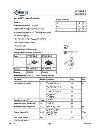
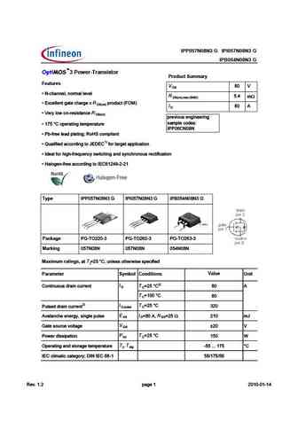
Type IPP055N03L G IPB055N03L G OptiMOS 3 Power-Transistor Product Summary Features V 30 V DS Fast switching MOSFET for SMPS R 5.5 m DS(on),max Optimized technology for DC/DC converters I 50 A D Qualified according to JEDEC1) for target applications N-channel, logic level Excellent gate charge x R product (FOM) DS(on) Very low on-resistance R DS(on
4.1. Size:730K infineon
ipp055n03l .pdf 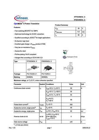
Type IPP055N03L G IPB055N03L G 3 Power-Transistor Product Summary Features V 30 V DS Fast switching MOSFET for SMPS R 5.5 mW DS(on),max Optimized technology for DC/DC converters I 50 A D Qualified according to JEDEC1) for target applications N-channel, logic level Excellent gate charge x R product (FOM) DS(on) Very low on-resistance R DS(on)
4.2. Size:250K inchange semiconductor
ipp055n03l.pdf 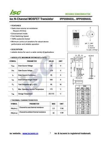
INCHANGE Semiconductor isc N-Channel MOSFET Transistor IPP055N03L IIPP055N03L FEATURES Static drain-source on-resistance RDS(on) 5.5m Enhancement mode Fast Switching Speed 100% avalanche tested Minimum Lot-to-Lot variations for robust device performance and reliable operation DESCRITION reliable device for use in a wide variety of applications ABSOLUTE
9.1. Size:1638K infineon
ipp051n15n5.pdf 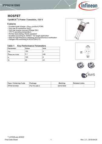
IPP051N15N5 MOSFET TO-220-3 OptiMOS 5 Power-Transistor, 150 V tab Features Excellent gate charge x R product (FOM) DS(on) Very low on-resistance R DS(on) Very low reverse recovery charge (Qrr) 175 C operating temperature Pb-free lead plating; RoHS compliant Qualified according to JEDEC1) for target application Ideal for high-frequency switching and s
9.2. Size:781K infineon
ipp05cn10n ipp05cn10n ipb05cn10n-g ipi05cn10n-g.pdf 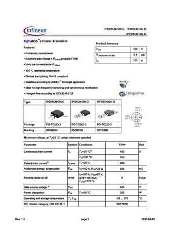
IPB05CN10N G IPI05CN10N G IPP05CN10N G 2 Power-Transistor Product Summary Features V 100 V DS R ( 492??6= ?@C>2= =6G6= R 5.1 m - @? >2I .) R I46==6?E 82E6 492C86 I R AC@5F4E !) ' DS(on) I 100 A D R /6CJ =@H @? C6D DE2?46 R DS(on) R U @A6C2E ?8 E6>A6C2EFC6 R *3 7C66 =625 A=2E ?8 , @#- 4@>A= 2?E 1) R + F2= 7 65 244@C5 ?8 E@ % 7@C E2C86E 2AA= 42E @? R $562= 7@C 9 89 7
9.3. Size:683K infineon
ipb049n06l3g ipp052n06l3g ipp052n06l3 ipb049n06l3 ipp052n06l3 ipb052n06l3.pdf 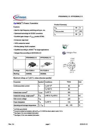
pe IPB049N06L3 G IPP052N06L3 G 3 Power-Transistor Product Summary Features V D R #562= 7@C 9 89 7C6BF6?4J DH E49 ?8 2?5 DJ?4 C64 R 4 7 m - @? >2I -' R ) AE > K65 E649?@=@8J 7@C 4@?G6CE6CD I D R I46==6?E 82E6 492C86 I R AC@5F4E ) ' D n) R ( 492??6= =@8 4 =6G6= R 2G2=2?496 E6DE65 R *3 7C66 A=2E ?8 , @"- 4@>A= 2?E 1) R + F2= 7 65 244@C5 ?8 E@ $ 7@C E2C86E 2AA= 42E
9.6. Size:563K infineon
ipp05cn10l2.pdf 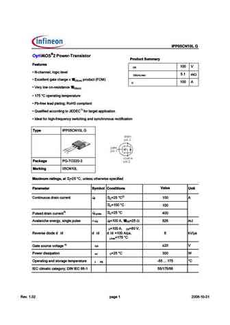
%% # ! % (>.;?6?@ %>E Features 1 D U ) 7
9.7. Size:526K infineon
ipp057n08n3-g ipi057n08n3-g ipb054n08n3-g.pdf 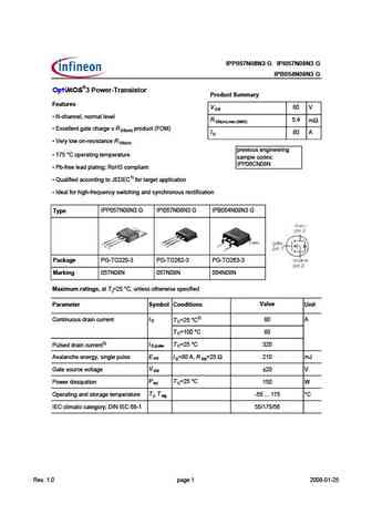
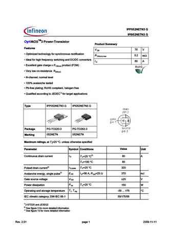
IPP057N08N3 G IPI057N08N3 G IPB054N08N3 G OptiMOS 3 Power-Transistor Product Summary Features V 80 V DS N-channel, normal level R 5.4 m DS(on),max (SMD) Excellent gate charge x R product (FOM) DS(on) I 80 A D Very low on-resistance R DS(on) previous engineering 175 C operating temperature sample codes IPP06CN08N Pb-free lead plating; RoHS complia
9.9. Size:875K infineon
ipp054ne8n.pdf 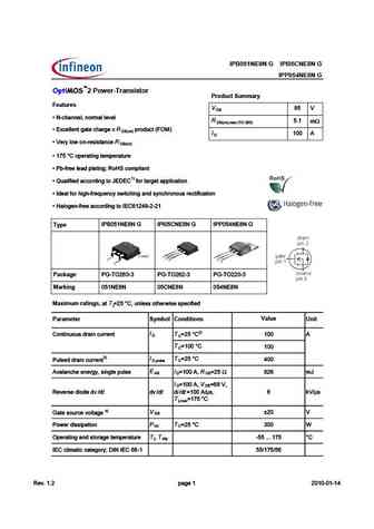
IPB051NE8N G IPI05CNE8N G IPP054NE8N G 2 Power-Transistor Product Summary Features V D R ( 492??6= ?@C>2= =6G6= R 1 m - @? >2I .) R I46==6?E 82E6 492C86 I R AC@5F4E !) ' D n) I 1 D R /6CJ =@H @? C6D DE2?46 R D n) R U @A6C2E ?8 E6>A6C2EFC6 R *3 7C66 =625 A=2E ?8 , @#- 4@>A= 2?E 1) R + F2= 7 65 244@C5 ?8 E@ % 7@C E2C86E 2AA= 42E @? R $562= 7@C 9 89 7C6BF6?4J DH E4
9.10. Size:731K infineon
ipb050n06ng ipp050n06ng.pdf 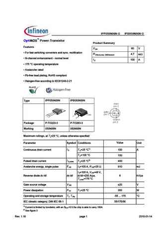
IPP050N06N G IPB050N06N G Power-Transistor Product Summary Features V D O >@ 50AB AE8B278=6 2>=D4@B4@A 0=3 AG=2 @42B85820B8>= R 4 7 m + >= = O ' 270==4; 4=70=24@?4@0B8=6 B4"+ 2>64= 5@44 022>@38=6 B> # Type #)) ' ' #) ' ' Package O O Mar
9.12. Size:689K infineon
ipb054n06n3g ipp057n06n3g.pdf 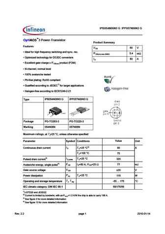
pe IPB054N06N3 G IPP057N06N3 G 3 Power-Transistor Product Summary Features V D Q #4513I CG9D389>7 1>4 CI>3 B53 R 4 m , ?> =1H ,& Q ( @D9=9J54 D538>?F5BD5BC I D Q H35>5?B=1
9.13. Size:503K infineon
ipb051ne8n-g ipi05cne8n-g ipp054ne8n-g.pdf 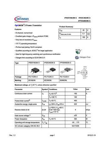
IPB051NE8N G IPI05CNE8N G IPP054NE8N G OptiMOS 2 Power-Transistor Product Summary Features V 85 V DS N-channel, normal level R 5.1 m DS(on),max (TO 263) Excellent gate charge x R product (FOM) DS(on) I 100 A D Very low on-resistance R DS(on) 175 C operating temperature Pb-free lead plating; RoHS compliant Qualified according to JEDEC1) for target
9.14. Size:1809K infineon
ipp052n08n5.pdf 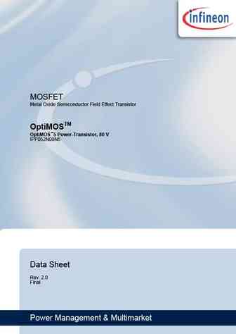
MOSFET Metal Oxide Semiconductor Field Effect Transistor OptiMOSTM OptiMOS 5 Power-Transistor, 80 V IPP052N08N5 Data Sheet Rev. 2.0 Final Power Management & Multimarket OptiMOS 5 Power-Transistor, 80 V IPP052N08N5 TO-220-3 1 Description tab Features Ideal for high frequency switching and sync. rec. Excellent gate charge x R product (FOM) DS(on) Very low on-resis
9.15. Size:1847K cn vbsemi
ipp052n06l3.pdf 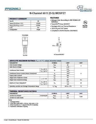
IPP052N06L3 www.VBsemi.tw N-Channel 60 V (D-S) MOSFET FEATURES PRODUCT SUMMARY Halogen-free According to IEC 61249-2-21 VDS (V) 60 Definition RDS(on) ( ) at VGS = 10 V 0.0035 TrenchFET Power MOSFET RDS(on) ( ) at VGS = 4.5 V 0.0090 Package with Low Thermal Resistance ID (A) 210 100 % Rg and UIS Tested Configuration Single Compliant to RoHS Directive 2002
9.16. Size:246K inchange semiconductor
ipp057n06n3.pdf 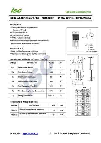
isc N-Channel MOSFET Transistor IPP057N06N3 IIPP057N06N3 FEATURES Static drain-source on-resistance RDS(on) 5.7m Enhancement mode Fast Switching Speed 100% avalanche tested Minimum Lot-to-Lot variations for robust device performance and reliable operation DESCRIPTION Ideal for high frequency switching Optimized technology for DC/DC converters ABSOLUTE M
9.17. Size:245K inchange semiconductor
ipp051n15n5.pdf 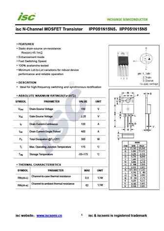
isc N-Channel MOSFET Transistor IPP051N15N5 IIPP051N15N5 FEATURES Static drain-source on-resistance RDS(on) 5.1m Enhancement mode Fast Switching Speed 100% avalanche tested Minimum Lot-to-Lot variations for robust device performance and reliable operation DESCRITION Ideal for high-frequency switching and synchronous rectification ABSOLUTE MAXIMUM RATINGS(T
9.18. Size:245K inchange semiconductor
ipp052n06l3.pdf 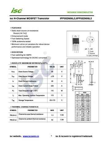
isc N-Channel MOSFET Transistor IPP052N06L3,IIPP052N06L3 FEATURES Static drain-source on-resistance RDS(on) 4.7m Enhancement mode Fast Switching Speed 100% avalanche tested Minimum Lot-to-Lot variations for robust device performance and reliable operation DESCRITION Fast switching for SMPS Optimized technology for DC/DC converters ABSOLUTE MAXIMUM RATINGS(
9.19. Size:246K inchange semiconductor
ipp052ne7n3.pdf 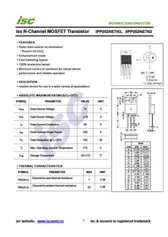
INCHANGE Semiconductor isc N-Channel MOSFET Transistor IPP052NE7N3 IIPP052NE7N3 FEATURES Static drain-source on-resistance RDS(on) 5.2m Enhancement mode Fast Switching Speed 100% avalanche tested Minimum Lot-to-Lot variations for robust device performance and reliable operation DESCRITION reliable device for use in a wide variety of applications ABSOLUTE M
9.20. Size:245K inchange semiconductor
ipp05cn10n.pdf 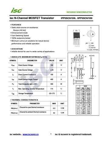
isc N-Channel MOSFET Transistor IPP05CN10N IIPP05CN10N FEATURES Static drain-source on-resistance RDS(on) 5.1m Enhancement mode Fast Switching Speed 100% avalanche tested Minimum Lot-to-Lot variations for robust device performance and reliable operation DESCRITION reliable device for use in a wide variety of applications ABSOLUTE MAXIMUM RATINGS(T =25 )
9.22. Size:245K inchange semiconductor
ipp057n08n3.pdf 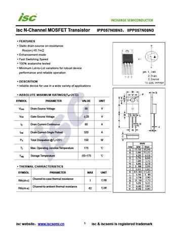
isc N-Channel MOSFET Transistor IPP057N08N3 IIPP057N08N3 FEATURES Static drain-source on-resistance RDS(on) 5.7m Enhancement mode Fast Switching Speed 100% avalanche tested Minimum Lot-to-Lot variations for robust device performance and reliable operation DESCRITION reliable device for use in a wide variety of applications ABSOLUTE MAXIMUM RATINGS(T =25
Другие IGBT... IPP042N03LG, IPP045N10N3G, IPP048N04NG, IPP048N12N3G, IPP04CN10NG, IPP04N03LBG, IPP052N06L3G, IPP052NE7N3G, IRF2807, IPP057N06N3G, IPP057N08N3G, IPP05CN10LG, IPP05CN10NG, IPP062NE7N3G, IPP065N03LG, IPP065N04NG, IPP065N06LG