BSS138 datasheet, аналоги, основные параметры
Наименование производителя: BSS138 📄📄
Тип транзистора: MOSFET
Полярность: N
Предельные значения
Pd ⓘ - Максимальная рассеиваемая мощность: 0.36 W
|Vds|ⓘ - Максимально допустимое напряжение сток-исток: 50 V
|Vgs|ⓘ - Максимально допустимое напряжение затвор-исток: 20 V
|Id| ⓘ - Максимально допустимый постоянный ток стока: 0.22 A
Tj ⓘ - Максимальная температура канала: 150 °C
Электрические характеристики
RDSonⓘ - Сопротивление сток-исток открытого транзистора: 3.5 Ohm
Тип корпуса: SOT23
📄📄 Копировать
Аналог (замена) для BSS138
- подборⓘ MOSFET транзистора по параметрам
BSS138 даташит
bss138 d87z bss138 l99z.pdf
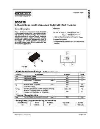
October 2005 BSS138 N-Channel Logic Level Enhancement Mode Field Effect Transistor Features General Description These N-Channel enhancement mode field effect 0.22 A, 50 V. RDS(ON) = 3.5 @ VGS = 10 V transistors are produced using Fairchild s proprietary, RDS(ON) = 6.0 @ VGS = 4.5 V high cell density, DMOS technology. These products have been designed to minimize
bss138.pdf
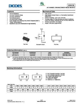
BSS138 N-CHANNEL ENHANCEMENT MODE MOSFET Features Mechanical Data Low On-Resistance Case SOT23 Low Gate Threshold Voltage Case Material Molded Plastic. UL Flammability Classification Low Input Capacitance Rating 94V-0 Fast Switching Speed Moisture Sensitivity Level 1 per J-STD-020 Low Input/Output Leakage Terminals Matte Tin Finish A
bss138.pdf
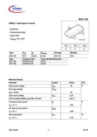
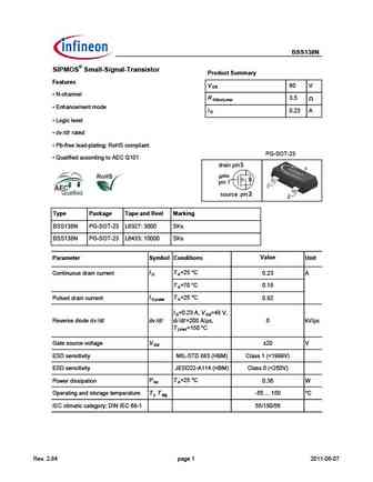
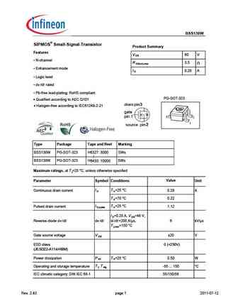
BSS 138 SIPMOS Small-Signal Transistor N channel Enhancement mode Logic Level VGS(th) = 0.8...2.0V Pin 1 Pin 2 Pin 3 G S D Type VDS ID RDS(on) Package Marking BSS 138 50 V 0.22 A 3.5 SOT-23 SSs Type Ordering Code Tape and Reel Information BSS 138 Q67000-S566 E6327 BSS 138 Q67000-S216 E6433 Maximum Ratings Parameter Symbol Values Unit Drain source voltage VD
bss138.pdf
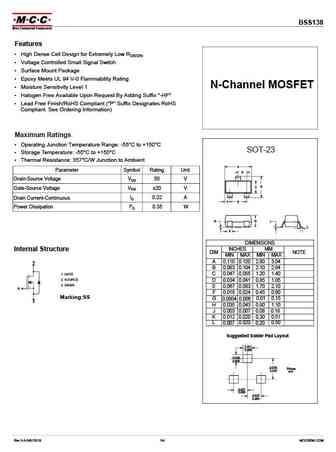
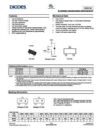
BSS138 Features High Dense Cell Design for Extremely Low RDS(ON) Voltage Controlled Small Signal Switch Surface Mount Package Epoxy Meets UL 94 V-0 Flammability Rating N-Channel MOSFET Moisture Sensitivity Level 1 Halogen Free Available Upon Request By Adding Suffix "-HF" Lead Free Finish/RoHS Compliant ("P" Suffix Designates RoHS Compliant. See Ordering In
bss138.pdf

October 2005 BSS138 N-Channel Logic Level Enhancement Mode Field Effect Transistor Features General Description These N-Channel enhancement mode field effect 0.22 A, 50 V. RDS(ON) = 3.5 @ VGS = 10 V transistors are produced using Fairchild s proprietary, RDS(ON) = 6.0 @ VGS = 4.5 V high cell density, DMOS technology. These products have been designed to minimize
bss138.pdf
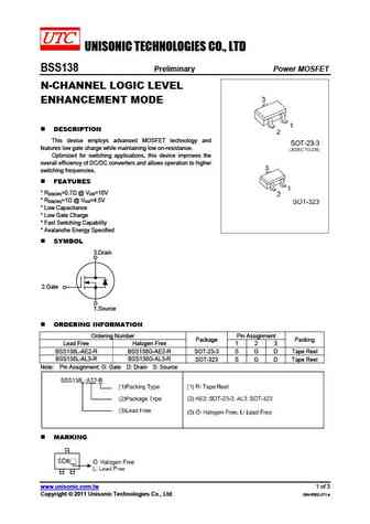
UNISONIC TECHNOLOGIES CO., LTD BSS138 Preliminary Power MOSFET N-CHANNEL LOGIC LEVEL ENHANCEMENT MODE DESCRIPTION This device employs advanced MOSFET technology and features low gate charge while maintaining low on-resistance. Optimized for switching applications, this device improves the overall efficiency of DC/DC converters and allows operation to higher switching frequenc
bss138.pdf
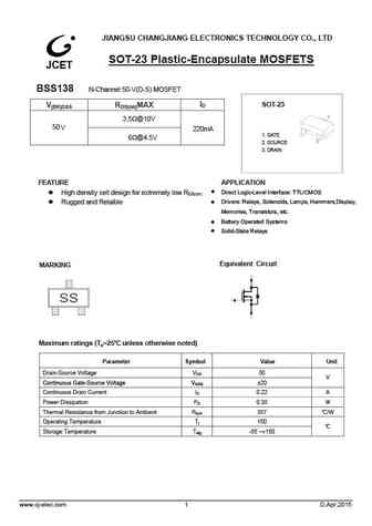
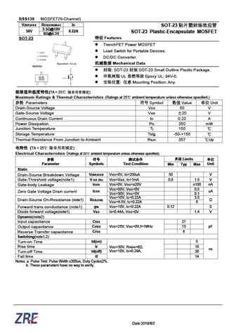
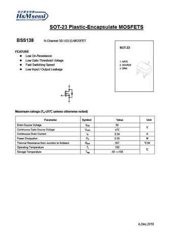
JIANGSU CHANGJIANG ELECTRONICS TECHNOLOGY CO., LTD SOT-23 Plastic-Encapsulate MOSFETS BSS138 N-Channel 50-V(D-S) MOSFET ID SOT-23 V(BR)DSS RDS(on)MAX 3.5 @10V 50 V 220mA 1. GATE 6 @4.5V 2. SOURCE 3. DRAIN FEATURE APPLICATION Direct Logic-Level Interface TTL/CMOS High density cell design for extremely low RDS(on) Rugged and Relaible Drivers Relays
bss138.pdf
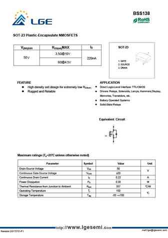
BSS138 SOT-23 Plastic-Encapsulate NMOSFETS ID SOT-23 V(BR)DSS RDS(on)MAX 3.5 @10V 50 V 220mA 1. GATE 6 @4.5V 2. SOURCE 3. DRAIN FEATURE APPLICATION Direct Logic-Level Interface TTL/CMOS High density cell design for extremely low RDS(on) Rugged and Relaible Drivers Relays, Solenoids, Lamps, Hammers,Display, Memories, Transistors, etc. Battery Operated Sys
bss138.pdf
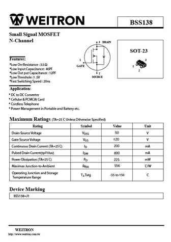
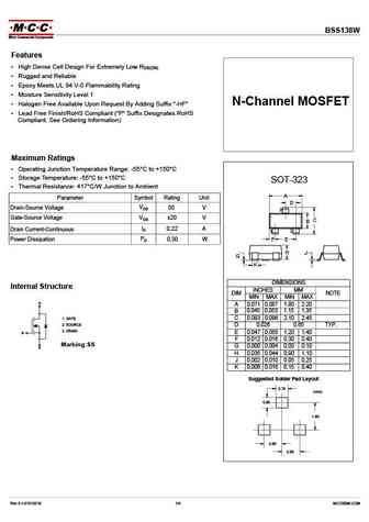
BSS138 Small Signal MOSFET N-Channel 3 DRAIN SOT-23 Features 3 1 *Low On-Resistance 3.5 GATE 1 *Low Input Capacitance 40PF 2 *Low Out put Capacitance 12PF 2 SOURCE *Low Threshole 1 .5V *Fast Switching Speed 20ns Application * DC to DC Converter * Cellular & PCMCIA Card * Cordless Telephone * Power Management in Portable and Battery etc. Maximum Ratings (TA
bss138.pdf
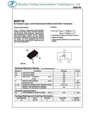
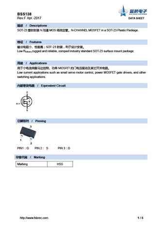
Shenzhen Tuofeng Semiconductor Technology Co., Ltd BSS138 BSS138 N-Channel Logic Level Enhancement Mode Field Effect Transistor Features General Description These N-Channel enhancement mode field effect 0.22 A, 50 V. RDS(ON) = 3.5 @ VGS = 10 V transistors are produced using Fairchild s proprietary, RDS(ON) = 6.0 @ VGS = 4.5 V high cell density, DMOS technology. Th
bss138.pdf
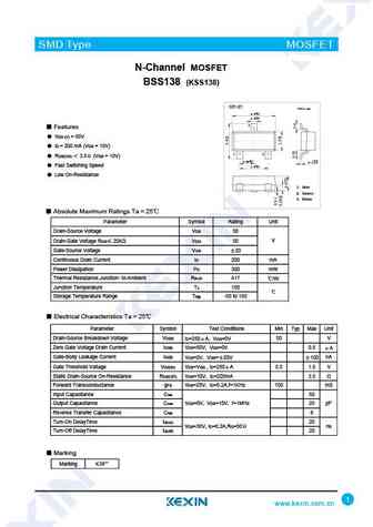
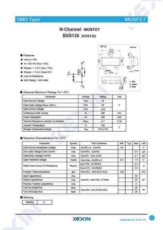
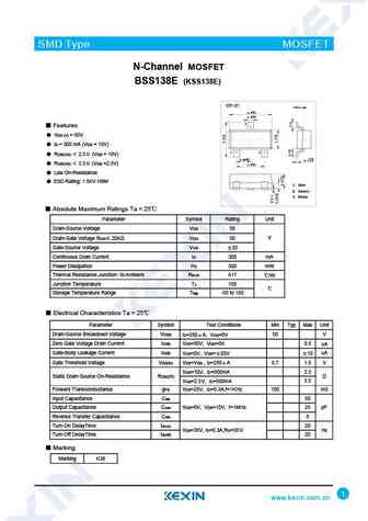
SMD Type MOSFET N-Channel MOSFET BSS138 (KSS138) SOT-23 Unit mm +0.1 2.9 -0.1 +0.1 0.4 -0.1 3 Features VDS (V) = 50V ID = 200 mA (VGS = 10V) 1 2 RDS(ON) 3.5 (VGS = 10V) +0.1 +0.05 0.95-0.1 0.1-0.01 +0.1 Fast Switching Speed 1.9-0.1 Low On-Resistance 1. Gate 2. Source 3. Drain Absolute Maximum Ratings Ta = 25 Parameter Symbol R
bss138.pdf
BSS138 50V N-Channel Enhancement Mode MOSFET - ESD Protected FEATURES RDS(ON), VGS@10V,IDS@500mA=3 RDS(ON), VGS@4.5V,IDS@200mA=4 0.120(3.04) RDS(ON), VGS@2.5V,IDS@100mA=6 0.110(2.80) Advanced Trench Process Technology High Density Cell Design For Ultra Low On-Resistance Very Low Leakage Current In Off Condition 0.056(1.40) 0.047(1.20) Specially Des
bss138.pdf
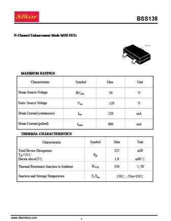
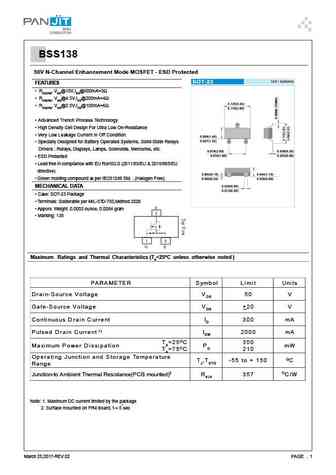
BSS138 N-Channel Enhancement-Mode MOS FETs N-Channel Enhancement-Mode MOS FETs N-Channel Enhancement-Mode MOS FETs N-Channel Enhancement-Mode MOS FETs MAXIMUM RATINGS MAXIMUM RATINGS MAXIMUM RATINGS MAXIMUM RATINGS Characteristic Symbol Max Unit Drain-Source Voltage BVDSS 50 V Gate- Source Voltage VGS +20 V Drain Current (continuous) IDR 220 mA Drain Current (pulsed) IDRM 880 m
bss138.pdf
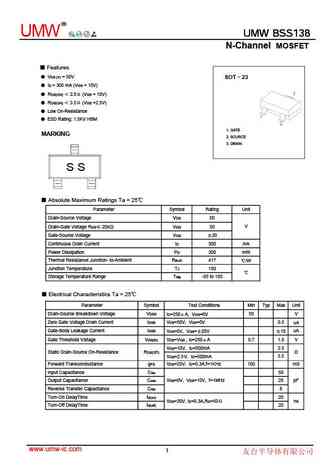
R UMWType UMW BSS138 UMW BSS138 UMW BSS138 SMD N-Channel MOSFET Features VDS (V) = 50V SOT 23 ID = 300 mA (VGS = 10V) RDS(ON) 2.5 (VGS = 10V) RDS(ON) 3.5 (VGS =2.5V) Low On-Resistance ESD Rating 1.5KV HBM 1. GATE MARKING 2. SOURCE 3. DRAIN S S Absolute Maximum Ratings Ta = 25 Parameter Symbol Rating Unit Drain-Source V
bss138.pdf
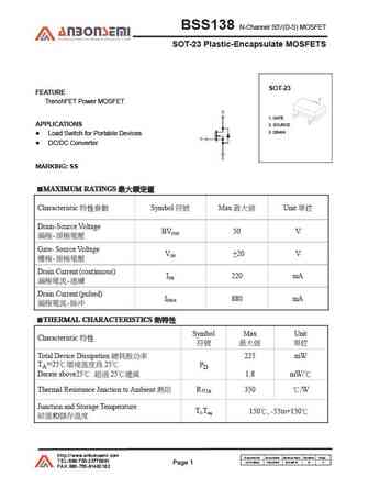
BSS138 N-Channel 50V(D-S) MOSFET SOT-23 Plastic-Encapsulate MOSFETS SOT-23 FEATURE TrenchFET Power MOSFET 1. GATE APPLICATIONS 2. SOURCE 3. DRAIN Load Switch for Portable Devices DC/DC Converter MARKING SS MAXIMUM RATINGS MAXIMUM RATINGS MAXIMUM RATINGS MAXIMUM RATINGS Characteristic Symbol Max Unit Drain-So
bss138.pdf
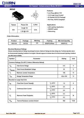
BSS138 MOSFET ROHS N-Channel Enhancement-Mode MOSFET SOT-23 - Features Low RDS(on) @VGS=10V 3.3V Logic Level Control N Channel SOT23 Package Pb-Free, RoHS Compliant V R Typ I Max (BR)DSS DS(ON) D Applications LED Lighting Application, 1 @ 10V ON/OFF switch 50V 0.5A 1.2 @ 4.5V Networking Order Information Marking Product Package P
bss138.pdf
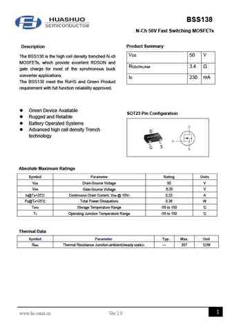
BSS138 N-Ch 50V Fast Switching MOSFETs Description Product Summary VDS 50 V The BSS138 is the high cell density trenched N-ch MOSFETs, which provide excellent RDSON and RDS(ON),max 3.4 gate charge for most of the synchronous buck converter applications. ID 230 mA The BSS138 meet the RoHS and Green Product requirement with full function reliability approved. Green
bss138.pdf
BSS138 MOSFET(N-Channel) V(BR)DSS RDS(ON)MAX ID SOT-23 3.5 @10V 50V 0.22A SOT-23 Plastic-Encapsulate MOSFET 6 @4.5V SOT-23 Features TrenchFET Power MOSFET Load Switch for Portable Devices. DC/DC Converter. Mechanical Data SOT-23 SOT-23 Small Outline Plastic Package. UL Epoxy
bss138.pdf
SHENZHEN LONG JING MICRO-ELECTRONICS CO., LTD. SOT-23 Plastic-Encapsulate Mosfets BSS138 N-Channel Mosfet Features High density cell design for extremely low R DS(on) Rugged and Reliable Application 1. Gate Direct Logic-Level Interface TTL/CMOS Drivers Relays, Solenoids, Lamps, Hammers, Display, Memories, 2. Source Transistors, etc. 3. Drain Battery Oper
bss138.pdf
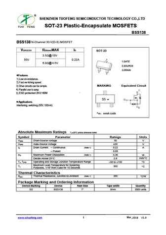
SHENZHEN TUOFENG SEMICONDUCTOR TECHNOLOGY CO.,LTD SOT-23 Plastic-Encapsulate MOSFETS BSS138 N-Channel 30-V(D-S) MOSFET BSS138 V(BR)DSS RDS(on)MAX ID SOT-23 3.5 @ 10V 3 50V 0.22A 1.GATE 6.0 @ 4.5V 2.SOURCE 3.DRAIN 1 2 Features 1) Low on-resistance. 2) Fast sw itching speed. MARKING Equivalent Circuit 3) Drive circuits can be simple. 4) Parallel use is easy. 5) ESD
bss138.pdf
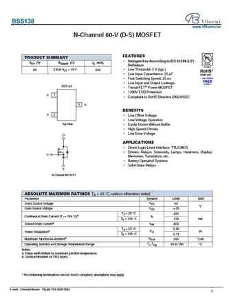
BSS138 www.VBsemi.tw N-Channel 60-V (D-S) MOSFET FEATURES PRODUCT SUMMARY Halogen-free According to IEC 61249-2-21 VDS (V) RDS(on) ( )ID (mA) Definition 2.8 at VGS = 10 V 60 250 Low Threshold 2 V (typ.) Low Input Capacitance 25 pF Fast Switching Speed 25 ns Low Input and Output Leakage SOT-23 TrenchFET Power MOSFET 1200V ESD Protection G 1
bss138.pdf
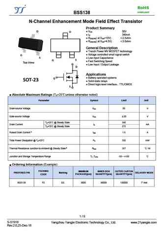
RoHS COMPLIANT BSS138 N-Channel Enhancement Mode Field Effect Transistor Product Summary V 50V DS I 340mA D R ( at V =10V) 2.5ohm DS(ON) GS R ( at V =4.5V) 3.0ohm DS(ON) GS General Description Trench Power MV MOSFET technology Voltage controlled small signal switch Low input Capacitance Fast Switching Speed Low Input / O
bss138.pdf
SOT-23 Plastic-Encapsulate MOSFETS BSS138 N-Channel 50-V(D-S) MOSFET SOT-23 FEATURE Low On-Resistance Low Gate Threshold Voltage 1. GATE Fast Switching Speed 2. SOURCE 3. DRAI Low Input / Output Leakage Maximum ratings (Ta=25 unless otherwise noted) Parameter Symbol Value Unit Drain-Source Voltage VDS 50 V Continuous Gate-Source Voltage VGSS 12 Continuous D
bss138k.pdf
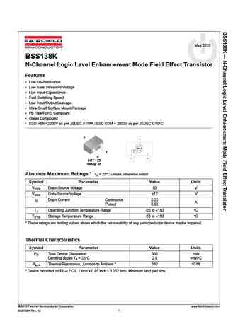
May 2010 BSS138K N-Channel Logic Level Enhancement Mode Field Effect Transistor Features Low On-Resistance Low Gate Threshold Voltage Low Input Capacitance Fast Switching Speed Low Input/Output Leakage Ultra-Small Surface Mount Package Pb Free/RoHS Compliant Green Compound ESD HBM=2000V as per JEDEC A114A ; ESD CDM = 2000V as per JEDEC C101C D S
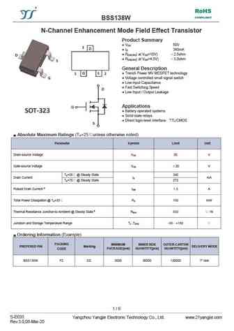
bss138w.pdf
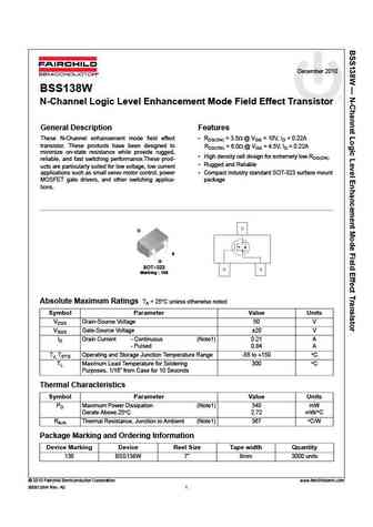
December 2010 BSS138W N-Channel Logic Level Enhancement Mode Field Effect Transistor General Description Features These N-Channel enhancement mode field effect RDS(ON) = 3.5 @ VGS = 10V, ID = 0.22A transistor. These products have been designed to RDS(ON) = 6.0 @ VGS = 4.5V, ID = 0.22A minimize on-state resistance while provide rugged, High density cell design for extremely
bss138bk.pdf
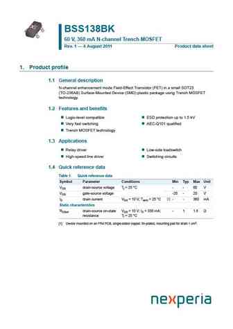
BSS138BK 60 V, 360 mA N-channel Trench MOSFET Rev. 1 4 August 2011 Product data sheet 1. Product profile 1.1 General description N-channel enhancement mode Field-Effect Transistor (FET) in a small SOT23 (TO-236AB) Surface-Mounted Device (SMD) plastic package using Trench MOSFET technology. 1.2 Features and benefits Logic-level compatible ESD protection up to 1.5 kV V
bss138aka.pdf
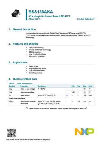
BSS138AKA 60 V, single N-channel Trench MOSFET 29 April 2015 Product data sheet 1. General description N-channel enhancement mode Field-Effect Transistor (FET) in a small SOT23 (TO-236AB) Surface-Mounted Device (SMD) plastic package using Trench MOSFET technology. 2. Features and benefits Very fast switching Trench MOSFET technology ESD protection Low threshold voltag
bss138bks.pdf
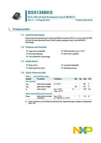
BSS138BKS 60 V, 320 mA dual N-channel Trench MOSFET Rev. 1 12 August 2011 Product data sheet 1. Product profile 1.1 General description Dual N-channel enhancement mode Field-Effect Transistor (FET) in a very small SOT363 (SC-88) Surface-Mounted Device (SMD) plastic package using Trench MOSFET technology. 1.2 Features and benefits Logic-level compatible ESD protection up t
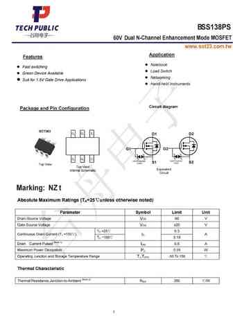
bss138ps.pdf
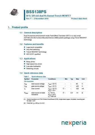
BSS138PS 60 V, 320 mA dual N-channel Trench MOSFET Rev. 1 2 November 2010 Product data sheet 1. Product profile 1.1 General description Dual N-channel enhancement mode Field-Effect Transistor (FET) in a very small SOT363 (SC-88) Surface-Mounted Device (SMD) plastic package using Trench MOSFET technology. 1.2 Features and benefits Logic-level compatible Very fast switching Tr
bss138pw.pdf
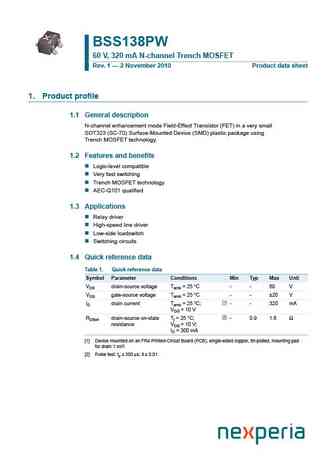
BSS138PW 60 V, 320 mA N-channel Trench MOSFET Rev. 1 2 November 2010 Product data sheet 1. Product profile 1.1 General description N-channel enhancement mode Field-Effect Transistor (FET) in a very small SOT323 (SC-70) Surface-Mounted Device (SMD) plastic package using Trench MOSFET technology. 1.2 Features and benefits Logic-level compatible Very fast switching Trench MOSFE
bss138p.pdf
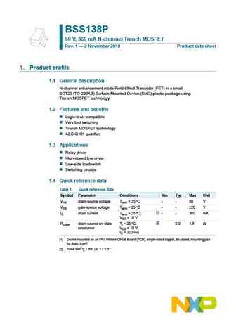
BSS138P 60 V, 360 mA N-channel Trench MOSFET Rev. 1 2 November 2010 Product data sheet 1. Product profile 1.1 General description N-channel enhancement mode Field-Effect Transistor (FET) in a small SOT23 (TO-236AB) Surface-Mounted Device (SMD) plastic package using Trench MOSFET technology. 1.2 Features and benefits Logic-level compatible Very fast switching Trench MOSFET te
bss138w.pdf
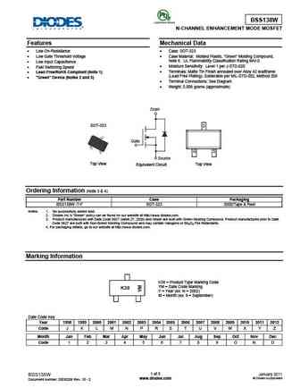
BSS138W N-CHANNEL ENHANCEMENT MODE MOSFET Features Mechanical Data Low On-Resistance Case SOT-323 Low Gate Threshold Voltage Case Material Molded Plastic, "Green" Molding Compound, Note 6. UL Flammability Classification Rating 94V-0 Low Input Capacitance Moisture Sensitivity Level 1 per J-STD-020 Fast Switching Speed Terminals Matte Tin Finish
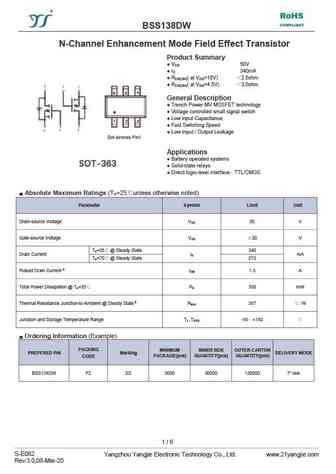
bss138dw.pdf
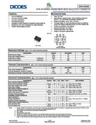
BSS138DW DUAL N-CHANNEL ENHANCEMENT MODE FIELD EFFECT TRANSISTOR Please click here to visit our online spice models database. Features Mechanical Data Low On-Resistance Case SOT-363 Low Gate Threshold Voltage Case Material Molded Plastic. Green Molding Compound (Note 6). UL Flammability Classification Rating 94V-0 Low Input Capacitance Moisture Sensi
bss138n.pdf
BSS138N SIPMOS Small-Signal-Transistor Product Summary Features V 60 V DS N-channel R 3.5 DS(on),max Enhancement mode I 0.23 A D Logic level dv /dt rated Pb-free lead-plating; RoHS compliant PG-SOT-23 Qualified according to AEC Q101 Type Package Tape and Reel Marking BSS138N PG-SOT-23 L6327 3000 SKs BSS138N PG-SOT-23 L6433 10000 SKs Parameter
bss138w.pdf
BSS138W SIPMOS Small-Signal-Transistor Product Summary Features V 60 V DS N-channel R 3.5 DS(on),max Enhancement mode I 0.28 A D Logic level dv /dt rated Pb-free lead-plating; RoHS compliant PG-SOT-323 Qualified according to AEC Q101 Halogen-free according to IEC61249-2-21 Type Package Tape and Reel Marking BSS138W PG-SOT-323 H SWs 6327 3
bss138akdw.pdf
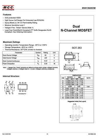
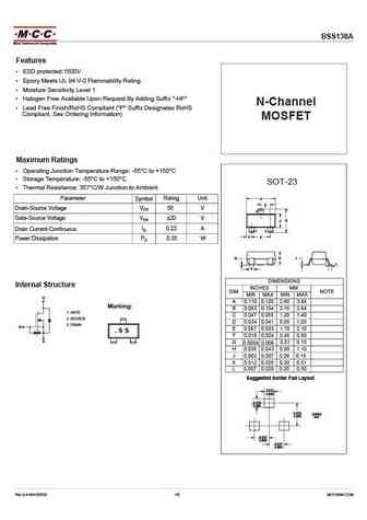
Features ESD protected 1500V High Dense Cell Design For Extremely Low RDS(ON) Epoxy Meets UL 94 V-0 Flammability Rating Moisture Sensitivity Level 1 Halogen Free. Green Device (Note 1) Lead Free Finish/RoHS Compliant ("P" Suffix Designates RoHS Compliant. See Ordering Information) Maximum Ratings Operating Junction
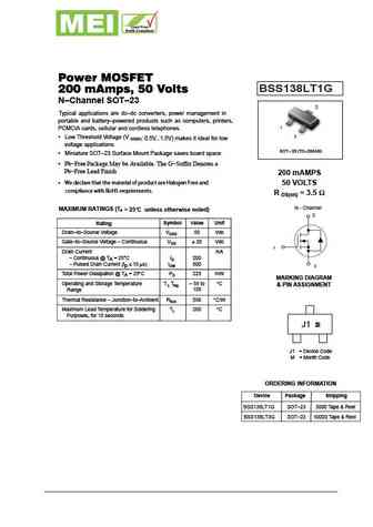
bss138lt1.pdf
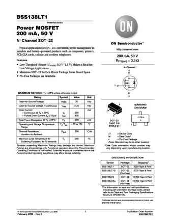
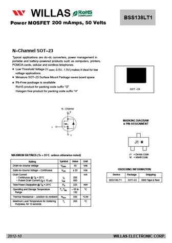
BSS138LT1 Preferred Device Power MOSFET 200 mA, 50 V N-Channel SOT-23 Typical applications are DC-DC converters, power management in http //onsemi.com portable and battery-powered products such as computers, printers, PCMCIA cards, cellular and cordless telephones. 200 mA, 50 V Features RDS(on) = 3.5 W Low Threshold Voltage (VGS(th) 0.5 V-1.5 V) Makes it Ideal for N-Channel L
bss138lt3 bss138lt3g.pdf

BSS138LT1 Power MOSFET 200 mA, 50 V N-Channel SOT-23 Typical applications are DC-DC converters, power management in http //onsemi.com portable and battery-powered products such as computers, printers, PCMCIA cards, cellular and cordless telephones. 200 mA, 50 V Features RDS(on) = 3.5 W Low Threshold Voltage (VGS(th) 0.5 V-1.5 V) Makes it Ideal for N-Channel Low Voltage Applica
bss138k.pdf

Is Now Part of To learn more about ON Semiconductor, please visit our website at www.onsemi.com Please note As part of the Fairchild Semiconductor integration, some of the Fairchild orderable part numbers will need to change in order to meet ON Semiconductor s system requirements. Since the ON Semiconductor product management systems do not have the ability to manage part nomenclatur
bss138l bvss138l.pdf
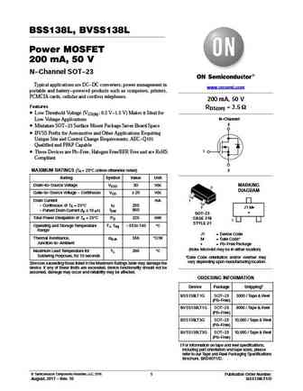
BSS138L, BVSS138L Power MOSFET 200 mA, 50 V N-Channel SOT-23 Typical applications are DC-DC converters, power management in www.onsemi.com portable and battery-powered products such as computers, printers, PCMCIA cards, cellular and cordless telephones. 200 mA, 50 V Features RDS(on) = 3.5 W Low Threshold Voltage (VGS(th) 0.5 V-1.5 V) Makes it Ideal for N-Channel Low Voltage Ap
bss138w.pdf
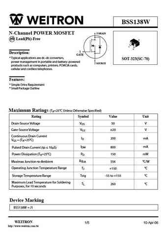
BSS138W 3 DRAIN N-Channel POWER MOSFET P b Lead(Pb)-Free 3 1 2 1 Description GATE * Typical applications are dc dc converters, SOT-323(SC-70) power management in portable and battery powered 2 SOURCE products such as computers, printers, PCMCIA cards, cellular and cordless telephones. Features * Simple Drive Requirement * Small Package Outline Maximum Ratings (TA=2
bss138lt1.pdf
FM120-M WILLAS THRU BSS 8LT1 200 mAmps, 50 Volts Power MOSFET FM1200-M 1.0A SURFACE MOUNT SCHOTTKY BARRIER RECTIFIERS -20V- 200V SOD-123 PACKAGE Pb Free Product Package outline Features Batch process design, excellent power dissipation offers better reverse leakage current and thermal resistance. SOD-123H Low profile surface mounted application in order to optim
bss138wt1.pdf
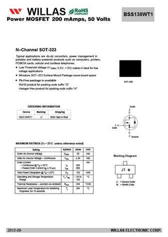
FM120-M WILLAS BSS138WT1 THRU 200 mAmps, 50 Volts Power MOSFET FM1200-M 1.0A SURFACE MOUNT SCHOTTKY BARRIER RECTIFIERS -20V- 200V SOD-123 PACKAGE Pb Free Product Package outline Features Batch process design, excellent power dissipation offers better reverse leakage current and thermal resistance. SOD-123H Low profile surface mounted application in order to optim
bss138c3.pdf
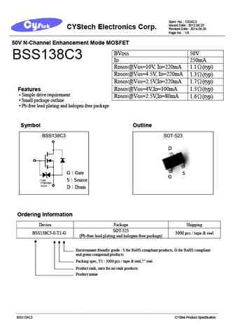
Spec. No. C834C3 Issued Date 2012.06.25 CYStech Electronics Corp. Revised Date 2014.08.20 Page No. 1/9 50V N-Channel Enhancement Mode MOSFET BVDSS 50V BSS138C3 ID 250mA RDSON@VGS=10V, ID=220mA 1.1 (typ) RDSON@VGS=4.5V, ID=220mA 1.3 (typ) RDSON@VGS=2.5V,ID=220mA 1.7 (typ) RDSON@VGS=4V,ID=100mA Features 1.3 (typ) Simple drive requirement RDSON@VGS=2.
lbss138wt1g s-lbss138wt1g.pdf
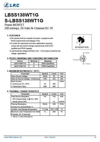
LBSS138WT1G S-LBSS138WT1G Power MOSFET 200 mAmps, 50 Volts N Channel SC-70 1. FEATURES We declare that the material of product compliance with RoHS requirements and Halogen Free. S- prefix for automotive and other applications requiring unique site and control change requirements; AEC-Q101 SC70(SOT-323) qualified and PPAP capable. Low threshold voltage (VGS(th)
lbss138lt1g s-lbss138lt1g.pdf
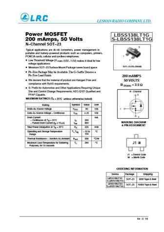
LESHAN RADIO COMPANY, LTD. Power MOSFET LBSS138LT1G 200 mAmps, 50 Volts S-LBSS138LT1G N Channel SOT 23 3 Typical applications are dc dc converters, power management in portable and battery powered products such as computers, printers, 1 PCMCIA cards, cellular and cordless telephones. 2 Low Threshold Voltage (V GS(th) 0.5V...1.5V) makes it ideal for low voltage applicat
bss138e-3.pdf
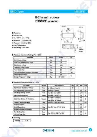
SMD Type MOSFET N-Channel MOSFET BSS138E (KSS138E) SOT-23-3 Unit mm +0.2 2.9 -0.1 +0.1 0.4 -0.1 3 Features VDS (V) = 50V ID = 300 mA (VGS = 10V) 1 2 +0.02 +0.1 RDS(ON) 2.5 (VGS = 10V) 0.15 -0.02 0.95 -0.1 +0.1 1.9 -0.2 RDS(ON) 3.5 (VGS =2.5V) Low On-Resistance ESD Rating 1.5KV HBM 1. Gate 2. Source 3. Drain Absolute M
bss138-3.pdf
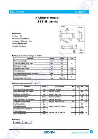
SMD Type MOSFET N-Channel MOSFET BSS138 (KSS138) SOT-23-3 Unit mm +0.2 2.9 -0.1 +0.1 0.4-0.1 3 Features VDS (V) = 50V ID = 200 mA (VGS = 10V) 1 2 +0.02 +0.1 0.15 -0.02 RDS(ON) 3.5 (VGS = 10V) 0.95 -0.1 +0.1 1.9 -0.2 Fast Switching Speed Low On-Resistance 1. Gate 2. Source 3. Drain Absolute Maximum Ratings Ta = 25 Parameter Sym
bss138e.pdf
SMD Type MOSFET N-Channel MOSFET BSS138E (KSS138E) SOT-23 Unit mm +0.1 2.9 -0.1 +0.1 0.4 -0.1 3 Features VDS (V) = 50V ID = 300 mA (VGS = 10V) 1 2 RDS(ON) 2.5 (VGS = 10V) +0.1 +0.05 0.95-0.1 0.1-0.01 +0.1 RDS(ON) 3.5 (VGS =2.5V) 1.9-0.1 Low On-Resistance ESD Rating 1.5KV HBM 1. Gate 2. Source 3. Drain Absolute Maximum
bss138-g.pdf
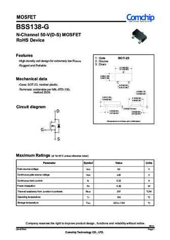
MOSFET BSS138-G N-Channel 50-V(D-S) MOSFET RoHS Device Features 1 Gate SOT-23 -High density cell design for extremely low RDS(ON). 2 Source 3 Drain -Rugged and Reliable. 0.118(3.00) 0.110(2.80) 3 0.055(1.40) 0.047(1.20) Mechanical data 1 2 -Case SOT-23, molded plastic. 0.079(2.00) 0.071(1.80) -Terminals solderable per MIL-STD-750, 0.006(0.15) method 2026. 0.
gsmbss138.pdf
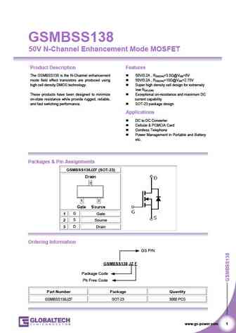
GSMBSS138 50V N-Channel Enhancement Mode MOSFET Product Description Features The GSMBSS138 is the N-Channel enhancement 50V/0.2A , RDS(ON)=3.5 @VGS=5V mode field effect transistors are produced using 50V/0.2A , RDS(ON)=10 @VGS=2.75V high cell density DMOS technology. Super high density cell design for extremely low RDS (ON) These products have been designed to min
bss138lt1g.pdf
Lead Free RoHS Compliant MEI BSS138LT1G N Channel SOT 23 3 Typical applications are dc dc converters, power management in portable and battery powered products such as computers, printers, 1 PCMCIA cards, cellular and cordless telephones. 2 Low Threshold Voltage (V GS(th) 0.5V...1.5V) makes it ideal for low voltage applications SOT 23 (TO 236AB) Miniatu
wstbss138.pdf
WSTBSS138 N-Ch MOSFET General Description Product Summery The WSTBSS138 is the highest performance BVDSS RDSON ID trench N-ch MOSFETs with extreme high cell density , which provide excellent RDSON and gate 110m 60V 2.1A charge for most of the synchronous buck converter applications . Applications The WSTBSS138 meet the RoHS and Green Product requirement , 100% EAS guara
bss138k.pdf
BSS138K www.VBsemi.tw N-Channel 60-V (D-S) MOSFET FEATURES PRODUCT SUMMARY Halogen-free According to IEC 61249-2-21 VDS (V) RDS(on) ( )ID (mA) Definition 2.8 at VGS = 10 V 60 250 Low Threshold 2 V (typ.) Low Input Capacitance 25 pF Fast Switching Speed 25 ns Low Input and Output Leakage SOT-23 TrenchFET Power MOSFET 1200V ESD Protection G 1
bss138w.pdf
BSS138W www.VBsemi.tw N-Channel 60-V (D-S) MOSFET FEATURES PRODUCT SUMMARY Halogen-free According to IEC 61249-2-21 VDS (V) RDS(on) ( )ID (mA) Definition 2 at VGS = 10 V 60 300 Low On-Resistance 2 Low Threshold 2 V (typ.) Low Input Capacitance 25 pF Fast Switching Speed 25 ns SOT-323 Low Input and Output Leakage SC-70 (3-LEADS) TrenchFET P
bss138dw.pdf
BSS138DW www.VBsemi.tw Dual N-Channel 60 V (D-S) MOSFET PRODUCT SUMMARY FEATURES VDS (V) RDS(on) ( )ID (mA) Halogen-free According to IEC 61249-2-21 Definition 2.5 at VGS = 10 V 60 300 Low On-Resistance 2.5 Low Threshold 2 V (typ.) Low Input Capacitance 25 pF Fast Switching Speed 25 ns SOT-363 Low Input and Output Leakage SC-70 TrenchFET
bss138w.pdf
RoHS COMPLIANT BSS138W N-Channel Enhancement Mode Field Effect Transistor Product Summary V 50V DS I 340mA D R ( at V =10V) 2.5ohm DS(ON) GS R ( at V =4.5V) 3.0ohm DS(ON) GS General Description Trench Power MV MOSFET technology Voltage controlled small signal switch Low input Capacitance Fast Switching Speed Low Input /
bss138dw.pdf
RoHS COMPLIANT BSS138DW N-Channel Enhancement Mode Field Effect Transistor Product Summary V 50V DS I 340mA D R ( at V =10V) 2.5ohm DS(ON) GS R ( at V =4.5V) 3.0ohm DS(ON) GS General Description Trench Power MV MOSFET technology Voltage controlled small signal switch Low input Capacitance Fast Switching Speed Low Input /
Другие IGBT... BSP92, BSR56, BSR57, BSR58, BSS100, BSS110, BSS123, BSS123A, BS170, BSS84, BUK100-50DL, BUK100-50GS, BUK101-50DL, BUK101-50GL, BUK101-50GS, BUK102-50DL, BUK102-50GL
Параметры MOSFET. Взаимосвязь и компромиссы
🌐 : EN ES РУ

Список транзисторов
Обновления
MOSFET: BPMS04N003M | BPM0405CG | BPM0306CG | BP0405SCG | B50T070F | B50T040F | BLM3404 | BL4N90 | SI2309S | SI2301F | BMSN3139 | BMS2302 | BMS2301 | BMDFN2302 | BMDFN2301 | BM8205
Popular searches
2n2222 data sheet | irf3205 datasheet | oc71 | njw0302g | 2n3904 transistor equivalent | 2sc2312 | bu406 datasheet | irfb7437