2SK3017. Аналоги и основные параметры
Наименование производителя: 2SK3017
Тип транзистора: MOSFET
Полярность: N
Предельные значения
Pd ⓘ
- Максимальная рассеиваемая мощность: 90 W
|Vds|ⓘ - Максимально допустимое напряжение сток-исток: 900 V
|Vgs|ⓘ - Максимально допустимое напряжение затвор-исток: 30 V
|Id| ⓘ - Максимально допустимый постоянный ток стока: 8.5 A
Tj ⓘ - Максимальная температура канала: 150 °C
Электрические характеристики
tr ⓘ -
Время нарастания: 25 ns
Cossⓘ - Выходная емкость: 220 pf
RDSonⓘ - Сопротивление сток-исток открытого транзистора: 1.25 Ohm
Тип корпуса: TO3P
Аналог (замена) для 2SK3017
- подборⓘ MOSFET транзистора по параметрам
2SK3017 даташит
..1. Size:724K toshiba
2sk3017.pdf 

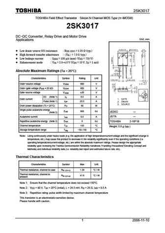
2SK3017 TOSHIBA Field Effect Transistor Silicon N Channel MOS Type ( -MOSIII) 2SK3017 DC-DC Converter, Relay Drive and Motor Drive Unit mm Applications Low drain-source ON resistance RDS (ON) = 1.05 (typ.) High forward transfer admittance Yfs = 7.0 S (typ.) Low leakage current IDSS = 100 A (max) (VDS = 720 V) Enhancement mode Vth = 2.0 4.0 V (VDS = 10
..2. Size:274K inchange semiconductor
2sk3017.pdf 

isc N-Channel MOSFET Transistor 2SK3017 FEATURES Drain Current I = 8.5A@ T =25 D C Drain Source Voltage V = 900V(Min) DSS Static Drain-Source On-Resistance R = 1.25 (Max) @V =10V DS(on) GS 100% avalanche tested Minimum Lot-to-Lot variations for robust device performance and reliable operation DESCRIPTION motor drive, DC-DC converter, power switch and solenoi
8.1. Size:340K 1
2sk3013.pdf 

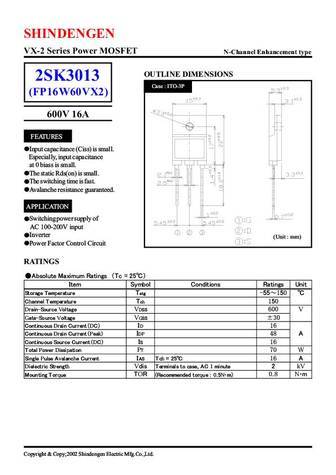
SHINDENGEN VX-2 Series Power MOSFET N-Channel Enhancement type OUTLINE DIMENSIONS 2SK3013 Case ITO-3P (FP16W60VX2) 600V 16A FEATURES Input capacitance (Ciss) is small. Especially, input capacitance at 0 biass is small. The static Rds(on) is small. The switching time is fast. Avalanche resistance guaranteed. APPLICATION Switching power supply of AC 100-200V input Inverter
8.2. Size:344K 1
2sk3012.pdf 

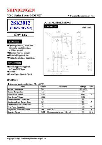
SHINDENGEN VX-2 Series Power MOSFET N-Channel Enhancement type OUTLINE DIMENSIONS 2SK3012 Case MTO-3P (Unit mm) (F16W60VX2) 600V 12A FEATURES Input capacitance (Ciss) is small. Especially, input capacitance at 0 biass is small. The static Rds(on) is small. The switching time is fast. Avalanche resistance guaranteed. APPLICATION Switching power supply of AC 100-200V input
8.3. Size:953K rohm
2sk3018ub.pdf 

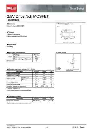
Data Sheet 2.5V Drive Nch MOSFET 2SK3018UB Structure Dimensions (Unit mm) Silicon N-channel MOSFET UMT3F 2.0 0.9 0.32 (3) Features 1) Low on-resistance. 2) Low voltage drive(2.5V drive). (1) (2) 0.65 0.65 0.13 1.3 Abbreviated symbol KN Application Switching Packaging specifications Inner circuit (3) Package Taping Type Code TCL Basic ordering u
8.4. Size:70K rohm
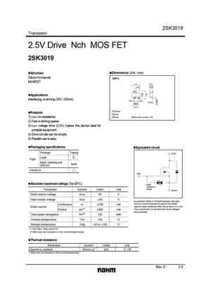
2sk3019.pdf 

2SK3019 Transistor 2.5V Drive Nch MOS FET 2SK3019 Dimensions (Unit mm) Structure Silicon N-channel EMT3 MOSFET 1.6 0.7 0.55 0.3 ( ) 3 Applications ( ) ( ) 2 1 Interfacing, switching (30V, 100mA) 0.2 0.2 0.15 0.5 0.5 1.0 (1)Source Features (2)Gate 1) Low on-resistance. (3)Drain Abbreviated symbol KN 2) Fast switching speed. 3) Low voltage drive (2.5
8.5. Size:79K rohm
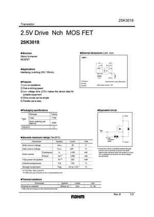
2sk3018.pdf 

2SK3018 Transistor 2.5V Drive Nch MOS FET 2SK3018 External dimensions (Unit mm) Structure Silicon N-channel UMT3 MOSFET 2.0 0.9 0.3 0.2 0.7 (3) Applications Interfacing, switching (30V, 100mA) (2) (1) 0.65 0.65 0.15 1.3 (1) Source Each lead has same dimensions Features (2) Gate Abbreviated symbol KN 1) Low on-resistance. (3) Drain 2) Fast switching s
8.6. Size:953K rohm
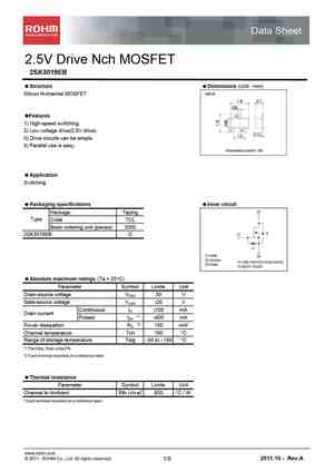
2sk3019eb.pdf 

Data Sheet 2.5V Drive Nch MOSFET 2SK3019EB Structure Dimensions (Unit mm) Silicon N-channel MOSFET EMT3F (3) Features 1) High-speed switching. (1) (2) 2) Low voltage drive(2.5V drive). 3) Drive circuits can be simple. 4) Parallel use is easy. Abbreviated symbol KN Application Switching Packaging specifications Inner circuit (3) Package Taping Type
8.7. Size:1125K mcc
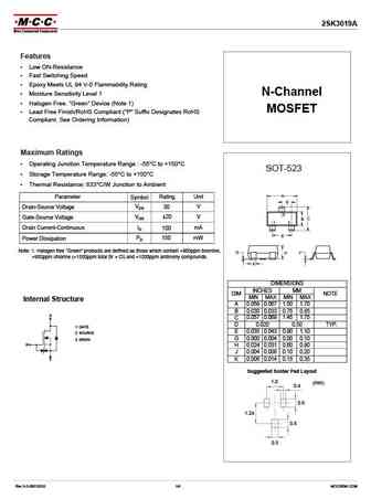
2sk3019a.pdf 

2SK3019A Features Low ON-Resistance Fast Switching Speed Epoxy Meets UL 94 V-0 Flammability Rating Moisture Sensitivity Level 1 N-Channel Halogen Free. Green Device (Note 1) MOSFET Lead Free Finish/RoHS Compliant ("P" Suffix Designates RoHS Compliant. See Ordering Information) Maximum Ratings Operating Junction Temperature Range -55 C to +150 C
8.8. Size:726K mcc
2sk3019.pdf 

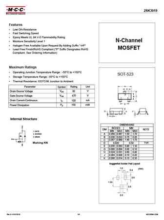
2SK3019 Features Low ON-Resistance Fast Switching Speed Epoxy Meets UL 94 V-0 Flammability Rating Moisture Sensitivity Level 1 N-Channel Halogen Free Available Upon Request By Adding Suffix "-HF" MOSFET Lead Free Finish/RoHS Compliant ("P" Suffix Designates RoHS Compliant. See Ordering Information) Maximum Ratings Operating Junction Temperature Range -55
8.9. Size:322K mcc
2sk3018.pdf 

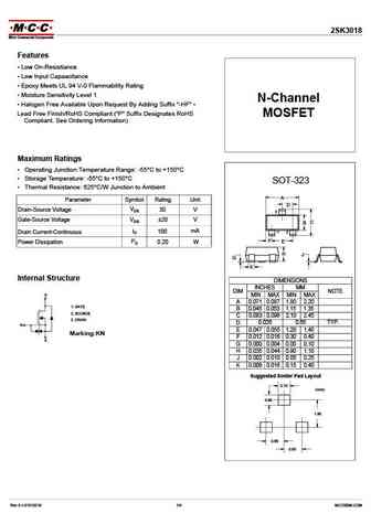
SK3018 Features Low On-Resistiance Low Input Capaacitance Maximum Ratings
8.10. Size:29K panasonic
2sk301.pdf 

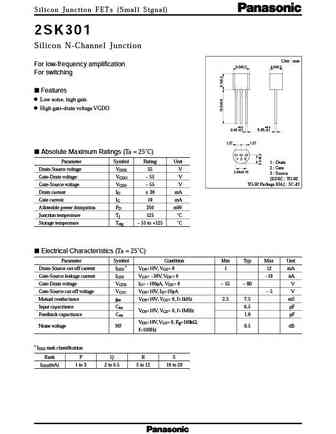
Silicon Junction FETs (Small Signal) 2SK301 2SK301 Silicon N-Channel Junction Unit mm For low-frequency amplification 5.0 0.2 4.0 0.2 For switching Features Low noise, high gain High gate-drain voltage VGDO +0.2 +0.2 0.45 0.1 0.45 0.1 1.27 1.27 Absolute Maximum Ratings (Ta = 25 C) 1 2 3 Parameter Symbol Rating Unit 1 Drain 2 Gate Drain-Source voltage VDSX
8.12. Size:1677K jiangsu
2sk3019.pdf 

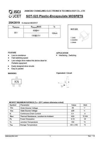
JIANGSU CHANGJING ELECTRONICS TECHNOLOGY CO., LTD SOT-523 Plastic-Encapsulate MOSFETS 2SK3019 N-channel MOSFET ID V(BR)DSS RDS(on)MAX SOT-523 8 @4V 30V 100mA 13 @2.5V 1. GATE 2. SOURCE 3. DRAIN FEATURE APPLICATION Low on-resistance Interfacing , Switching Fast switching speed Low voltage drive makes this device ideal for Portable equipment Easily des
8.13. Size:1362K jiangsu
2sk3018.pdf 

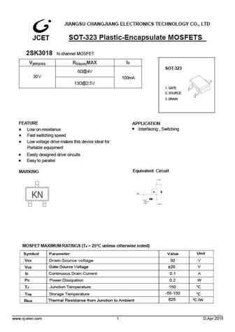
JIANGSU CHANGJIANG ELECTRONICS TECHNOLOGY CO., LTD SOT-323 Plastic-Encapsulate MOSFETS 2SK3018 N-channel MOSFET ID V(BR)DSS RDS(on)MAX SOT-323 8 @4V 30V 100mA 13 @2.5V 1. GATE 2. SOURCE 3. DRAIN FEATURE APPLICATION Interfacing , Switching Low on-resistance Fast switching speed Low voltage drive makes this device ideal for Portable equipment
8.14. Size:979K htsemi
2sk3018.pdf 

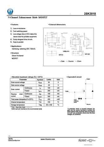
2SK3018 N-Channel Enhancement Mode MOSFET Features External dimensions 1) Low on-resistance. 2) Fast switching speed. 3) Low voltage drive (2.5V) makes this device ideal for portable equipment. 4) Easily designed drive circuits. 5) Easy to parallel. Applications Interfacing, switching (30V, 100mA) Units mm Structure SOT-323 S
8.15. Size:298K gsme
2sk3018.pdf 

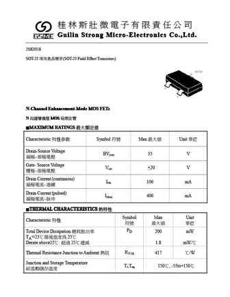
Guilin Strong Micro-Electronics Co.,Ltd. Guilin Strong Micro-Electronics Co.,Ltd. Guilin Strong Micro-Electronics Co.,Ltd. Guilin Strong Micro-Electronics Co.,Ltd. 2SK3018 SOT-23 (SOT-23 Field Effect Transistors) N-Channel Enhancement-Mode MOS FETs N-Channel Enhancement-Mode MOS FETs N-Channel Enhancement-Mode MOS FE
8.16. Size:705K wietron
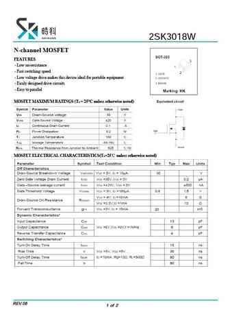
2sk3018w.pdf 

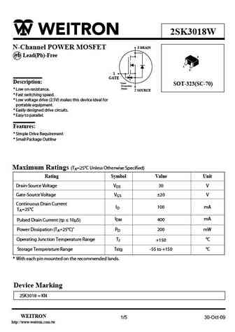
2SK3018W 3 DRAIN N-Channel POWER MOSFET P b Lead(Pb)-Free 3 1 2 1 GATE Description *Gate SOT-323(SC-70) Protection Diode * Low on-resistance. 2 SOURCE * Fast switching speed. * Low voltage drive (2.5V) makes this device ideal for portable equipment. * Easily designed drive circuits. * Easy to parallel. Features * Simple Drive Requirement * Small Package Outline Maxi
8.17. Size:709K wietron
2sk3019t.pdf 

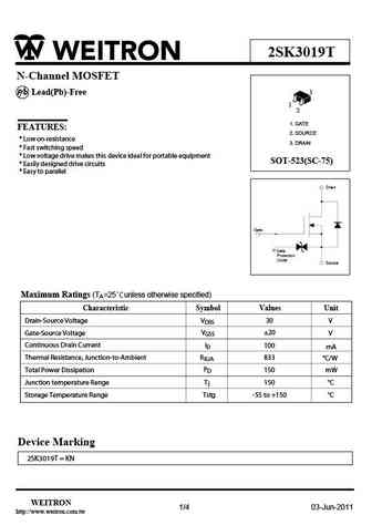
2SK3019T N-Channel MOSFET 3 P b Lead(Pb)-Free 1 2 1. GATE FEATURES 2. SOURCE * Low on-resistance 3. DRAIN * Fast switching speed * Low voltage drive makes this device ideal for portable equipment SOT-523(SC-75) * Easily designed drive circuits * Easy to parallel Maximum Ratings (TA=25 Cunless otherwise specified) Characteristic Symbol Values Unit Drain-Source Voltage VDSS 3
8.18. Size:475K willas
2sk3018lt1.pdf 

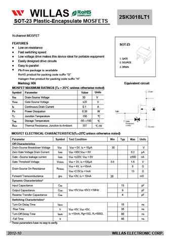
FM120-M WILLAS THRU 2SK3018LT1 SOT-23 Plastic-Encapsulate MOSFETS FM1200-M 1.0A SURFACE MOUNT SCHOTTKY BARRIER RECTIFIERS -20V- 200V SOD-123 PACKAGE Pb Free Product Package outline N-channel MOSFET Features Batch process design, excellent power dissipation offers better reverse leakage current and thermal resistance. SOD-123H FEATURES le surface mounted application i
8.19. Size:485K willas
2sk3019tt1.pdf 

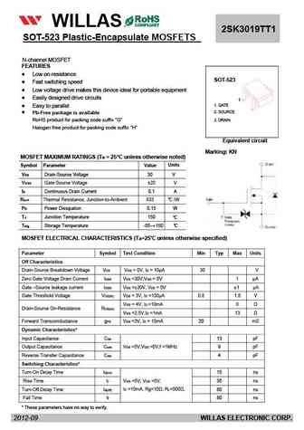
FM120-M WILLAS THRU 2SK3019TT1 SOT-523 Plastic-Encapsulate MOSFETS FM1200-M 1.0A SURFACE MOUNT SCHOTTKY BARRIER RECTIFIERS -20V- 200V SOD-123 PACKAGE Pb Free Product Package outline N-channel MOSFET Features FEATURES Batch process design, excellent power dissipation offers better reverse leakage current and thermal resistance. SOD-123H Low on-resistance Low
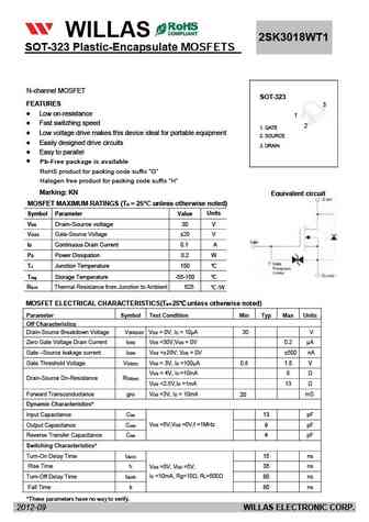
8.20. Size:467K willas
2sk3018wt1.pdf 

FM120-M WILLAS 2SK3018WT1 THRU SOT-323 Plastic-Encapsulate MOSFETS FM1200-M 1.0A SURFACE MOUNT SCHOTTKY BARRIER RECTIFIERS -20V- 200V SOD-123 PACKAGE Pb Free Product Package outline Features Batch process design, excellent power dissipation offers better rMOSFET N-channel everse leakage current and thermal resistance. SOD-123H Low profile surface mounted applicat
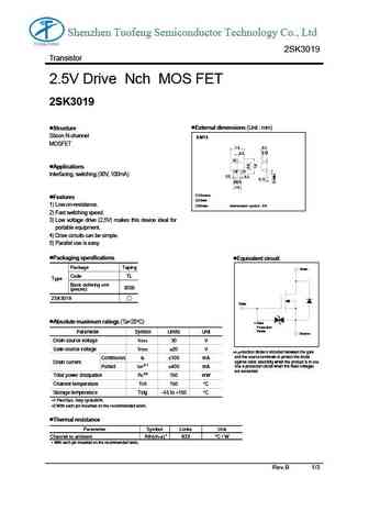
8.21. Size:574K shenzhen
2sk3019.pdf 

Shenzhen Tuofeng Semiconductor Technology Co., Ltd 2SK3019 Transistor 2.5V Drive Nch MOS FET 2SK3019 External dimensions (Unit mm) Structure Silicon N-channel EMT3 MOSFET 1.6 0.7 0.55 0.3 ( ) 3 Applications ( ) ( ) 2 1 Interfacing, switching (30V, 100mA) 0.2 0.2 0.15 0.5 0.5 1.0 (1)Source Features (2)Gate 1) Low on-resistance. (3)Drain Abbreviated sym
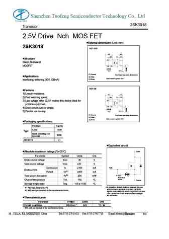
8.22. Size:1699K shenzhen
2sk3018.pdf 

Shenzhen Tuofeng Semiconductor Technology Co., Ltd 2SK3018 Transistor 2.5V Drive Nch MOS FET External dimensions (Unit mm) 2SK3018 SOT-323 2.0 0.9 0.3 0.2 0.7 Structure (3) Silicon N-channel MOSFET (2) (1) 0.65 0.65 0.15 1.3 (1) Source Each lead has same dimensions Applications (2) Gate Abbreviated symbol KN (3) Drain Interfacing, switching (30V, 100mA) SO
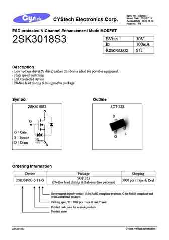
8.23. Size:317K cystek
2sk3018s3.pdf 

Spec. No. C800S3 Issued Date 2010.07.19 CYStech Electronics Corp. Revised Date 2013.12.10 Page No. 1/8 ESD protected N-Channel Enhancement Mode MOSFET BVDSS 30V 2SK3018S3 ID 100mA 8 RDSON(MAX) Description Low voltage drive(2V drive) makes this device ideal for portable equipment. High speed switching ESD protected device Pb-free lead pla
8.24. Size:320K cystek
2sk3019c3.pdf 

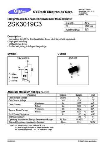
Spec. No. C800C3 Issued Date 2011.01.19 CYStech Electronics Corp. Revised Date Page No. 1/8 ESD protected N-Channel Enhancement Mode MOSFET BVDSS 30V 2SK3019C3 ID 100mA 8 RDSON(MAX) Description Low voltage drive(2.5V drive) makes this device ideal for portable equipment. High speed switching ESD protected device Pb-free lead plating & ha
8.25. Size:1094K blue-rocket-elect
2sk3018w.pdf 

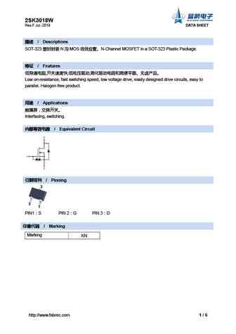
2SK3018W Rev.F Jul.-2019 DATA SHEET / Descriptions SOT-323 N MOS N-Channel MOSFET in a SOT-323 Plastic Package. / Features , , , Low on-resistance, fast switching speed, low voltage drive, easily designed drive circuits, easy to parallel. Halo
8.26. Size:1101K blue-rocket-elect
2sk3018.pdf 

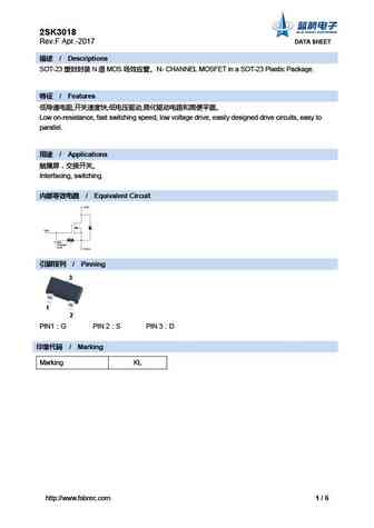
2SK3018 Rev.F Apr.-2017 DATA SHEET / Descriptions SOT-23 N MOS N- CHANNEL MOSFET in a SOT-23 Plastic Package. / Features , , , Low on-resistance, fast switching speed, low voltage drive, easily designed drive circuits, easy to parallel. / Applicatio
8.27. Size:311K lrc
l2sk3018wt1g s-l2sk3018wt1g.pdf 

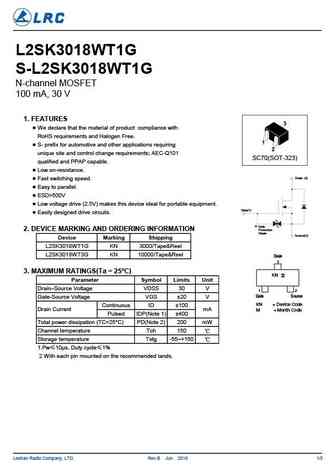
L2SK3018WT1G S-L2SK3018WT1G N-channel MOSFET 100 mA, 30 V 1. FEATURES We declare that the material of product compliance with RoHS requirements and Halogen Free. S- prefix for automotive and other applications requiring unique site and control change requirements; AEC-Q101 SC70(SOT-323) qualified and PPAP capable. Low on-resistance. Drain (3) Fast switching sp
8.28. Size:558K lrc
l2sk3019lt1g.pdf 

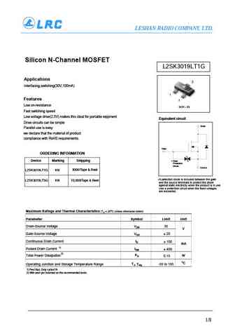
LESHAN RADIO COMPANY, LTD. Silicon N-Channel MOSFET L2SK3019LT1G Applications 3 Interfacing,switching(30V,100mA) 1 Features 2 Low on-resistance SOT 23 Fast switching speed Low voltage drive(2.5V) makes this ideal for portable equipment Equivalent circuit Drive circuits can be simple Drain Parallel use is easy we declare that the material of product compliance with RoHS
8.29. Size:97K lrc
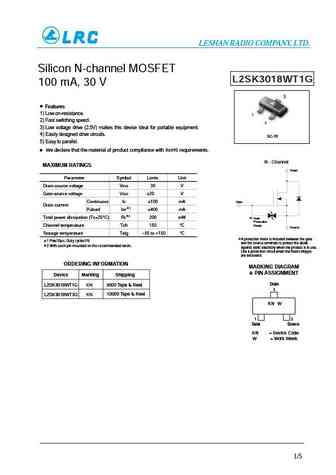
l2sk3018wt1g.pdf 

LESHAN RADIO COMPANY, LTD. Silicon N-channel MOSFET L2SK3018WT1G 100 mA, 30 V 3 Features 1) Low on-resistance. 1 2) Fast switching speed. 2 3) Low voltage drive (2.5V) makes this device ideal for portable equipment. 4) Easily designed drive circuits. SC-70 5) Easy to parallel. We declare that the material of product compliance with RoHS requirements. N - Channel MAX
8.30. Size:1097K kexin
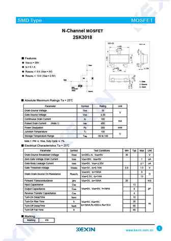
2sk3018-3.pdf 

SMD Type MOSFET N-Channel MOSFET 2SK3018 SOT-23-3 Unit mm +0.2 2.9 -0.1 +0.1 0.4 -0.1 3 Features VDS (V) = 30V Drain ID = 0.1 A 1 2 RDS(ON) 8 (VGS = 4V) +0.02 +0.1 0.15 -0.02 0.95 -0.1 +0.1 1.9 -0.2 RDS(ON) 13 (VGS = 2.5V) Gate 1. Gate Gate 2. Source Protection Diode 3. Drain Source Absolute Maximum Ratings Ta = 25 Par
8.31. Size:969K kexin
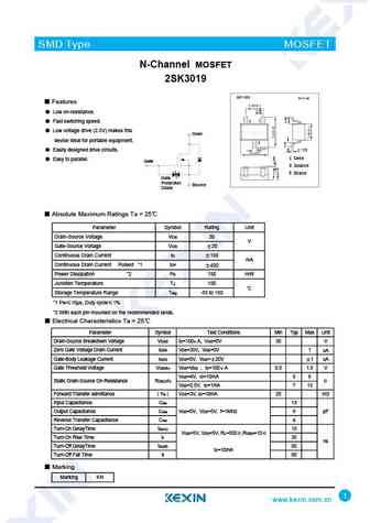
2sk3019.pdf 

SMD Type MOSFET N-Channel MOSFET 2SK3019 Features Low on-resistance. Fast switching speed. Low voltage drive (2.5V) makes this Drain device ideal for portable equipment. Easily designed drive circuits. 1 Gate Easy to parallel. Gate 2 Source 3 Drain Gate Protection Source Diode Absolute Maximum Ratings Ta = 25 Parameter Symbol Rating Uni
8.32. Size:799K kexin
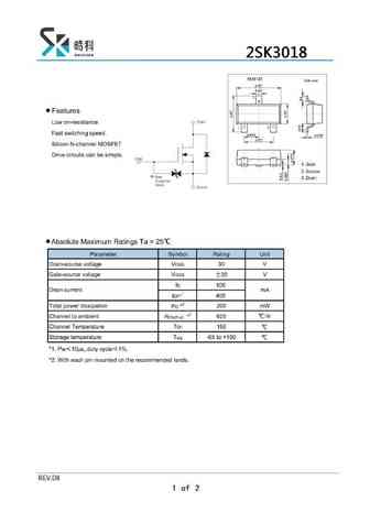
2sk3018.pdf 

SMD Type MOSFET N-Channel MOSFET 2SK3018 SOT-23 Unit mm +0.1 2.9-0.1 +0.1 0.4 -0.1 3 Features VDS (V) = 30V 1 2 Drain ID = 0.1 A +0.1 +0.05 0.95 -0.1 0.1 -0.01 1.9+0.1 -0.1 RDS(ON) 8 (VGS = 4V) RDS(ON) 13 (VGS = 2.5V) Gate 1. Gate 2. Source Gate 3. Drain Protection Diode Source Absolute Maximum Ratings Ta = 25 Parameter
8.33. Size:1941K slkor
2sk3018w.pdf 

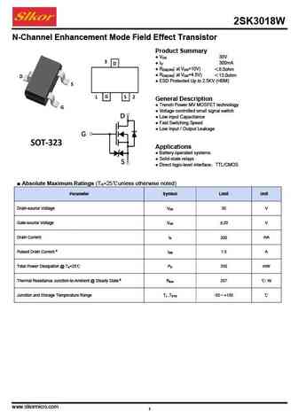
2SK3018W N-Channel Enhancement Mode Field Effect Transistor Product Summary V 30V DS I 300mA D R ( at V =10V) 8.0ohm DS(ON) GS R ( at V =4.5V) 13.0ohm DS(ON) GS ESD Protected Up to 2.5KV (HBM) General Description Trench Power MV MOSFET technology Voltage controlled small signal switch Low input Capacitance Fast Switching Speed Low
8.34. Size:484K slkor
2sk3018.pdf 

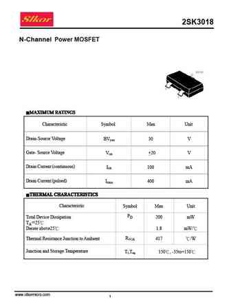
2SK3018 N-Channel Power MOSFET MAXIMUM RATINGS MAXIMUM RATINGS MAXIMUM RATINGS MAXIMUM RATINGS Characteristic Symbol Max Unit Drain-Source Voltage BVDSS 30 V Gate- Source Voltage VGS +20 V Drain Current (continuous) IDR 100 mA Drain Current (pulsed) IDRM 400 mA THERMAL CHARACTERISTICS THERMAL CHARACTERISTICS THERMAL CHARACTERISTICS THERMAL CHARACTERISTICS Characteristi
8.35. Size:388K guangdong hottech
2sk3018.pdf 

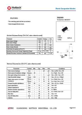
Plastic-Encapsulate Mosfets 2SK3018 FEATURES N-Channel MOSFET Fast switching speed and low on-resistance. Easily designed drived circuits. Absolute Maximum Ratings (TA=25oC, unless otherwise noted) 1.Gate 2.Source SOT-23 Parameter Symbol Ratings Unit 3.Drain VDS 30 Drain-Source Voltage V VGS Gate-source Voltage V 20 Drain ID Drain Current (Continuous) 100 mA IDM Dra
8.36. Size:1465K cn shikues
2sk3019.pdf 

2SK3019 N-channel MOSFET SOT-523 FEATURES 3 Low on-resistance 1 Fast switching speed 1. GATE Low voltage drive makes this device ideal for portable equipment 2 2. SOURCE Easily designed drive circuits 3. DRAIN Easy to parallel Marking KN Equivalent circuit MOSFET MAXIMUM RATINGS (Ta = 25 C unless otherwise noted) Units Symbol Parameter Value VDS D
8.37. Size:387K cn shikues
2sk3018w.pdf 

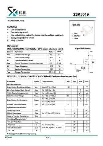
2SK3018W N-channel MOSFET FEATURES Low on-resistance Fast switching speed Low voltage drive makes this device ideal for portable equipment Low voltage drive makes this device ideal for portable equipment Easily designed drive circuits Easy to parallel MOSFET MAXIMUM RATINGS (Ta = 25 C unless otherwise noted) = 25 C unless otherwise noted) MOSFET ELECTRICAL CHARACT
8.39. Size:208K cn tak cheong
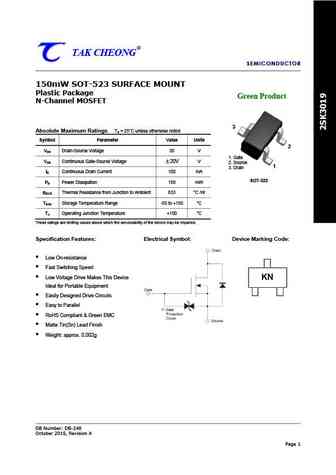
2sk3019.pdf 

TAK CHEONG SEMICONDUCTOR 150mW SOT-523 SURFACE MOUNT Plastic Package Green Product N-Channel MOSFET 3 Absolute Maximum Ratings TA = 25 C unless otherwise noted Symbol Parameter Value Units 2 VDS Drain-Source Voltage 30 V 1. Gate VGS Continuous Gate-Source Voltage 20V V 2. Source 1 3. Drain ID Continuous Drain Current 100 mA SOT-523 PD Power Dissipation 1
8.40. Size:2775K cn tuofeng
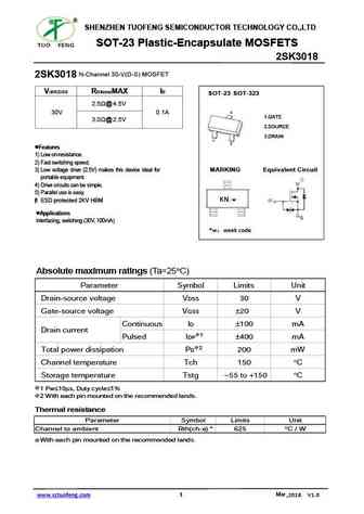
2sk3018.pdf 

SHENZHEN TUOFENG SEMICONDUCTOR TECHNOLOGY CO.,LTD SOT-23 Plastic-Encapsulate MOSFETS 2SK3018 N-Channel 30-V(D-S) MOSFET 2SK3018 V(BR)DSS RDS(on)MAX ID SOT-23 SOT-323 2.5 @ 4.5V 3 30V 0.1A 1.GATE 3.0 @ 2.5V 2.SOURCE 3.DRAIN 1 2 Features 1) Low on-resistance. 2) Fast switching speed. 3) Low voltage drive (2.5V) makes this device ideal for MARKING Equivalent Circuit por
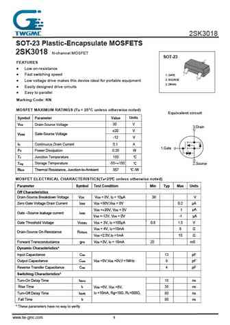
8.41. Size:810K cn twgmc
2sk3018.pdf 

MMBT5551 2SK3018 AO3400 SI2305 SOT-23 Plastic-Encapsulate MOSFETS 2SK3018 N-channel MOSFET SOT-23 FEATURES Low on-resistance Fast switching speed 1. GATE 2. SOURCE Low voltage drive makes this device ideal for portable equipment 3. DRAIN Easily designed drive circuits Easy to parallel Marking KN MOSFET MAXIMUM RATINGS (Ta = 25 C unless otherwise noted)
8.42. Size:274K inchange semiconductor
2sk3013.pdf 
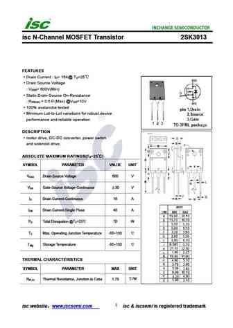
isc N-Channel MOSFET Transistor 2SK3013 FEATURES Drain Current I = 16A@ T =25 D C Drain Source Voltage V = 600V(Min) DSS Static Drain-Source On-Resistance R = 0.6 (Max) @V =10V DS(on) GS 100% avalanche tested Minimum Lot-to-Lot variations for robust device performance and reliable operation DESCRIPTION motor drive, DC-DC converter, power switch and solenoid
8.43. Size:330K inchange semiconductor
2sk3012.pdf 
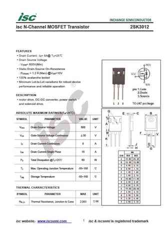
isc N-Channel MOSFET Transistor 2SK3012 FEATURES Drain Current I = 8A@ T =25 D C Drain Source Voltage V = 600V(Min) DSS Static Drain-Source On-Resistance R = 1.2 (Max) @V =10V DS(on) GS 100% avalanche tested Minimum Lot-to-Lot variations for robust device performance and reliable operation DESCRIPTION motor drive, DC-DC converter, power switch and solenoid d
Другие IGBT... 2SK2953, 2SK2962, 2SK2963, 2SK2964, 2SK2968, 2SK2989, 2SK2992, 2SK2998, RFP50N06, 2SK3132, 2SK3301, 2SK3371, 2SK3373, 2SK3438, 2SK3453, 2SK3466, 2SK3471
