3N90. Аналоги и основные параметры
Наименование производителя: 3N90
Тип транзистора: MOSFET
Полярность: N
Предельные значения
Pd ⓘ - Максимальная рассеиваемая мощность: 90 W
|Vds|ⓘ - Максимально допустимое напряжение сток-исток: 900 V
|Vgs|ⓘ - Максимально допустимое напряжение затвор-исток: 30 V
|Id| ⓘ - Максимально допустимый постоянный ток стока: 3 A
Tj ⓘ - Максимальная температура канала: 150 °C
Электрические характеристики
tr ⓘ - Время нарастания: 25 ns
Cossⓘ - Выходная емкость: 63 pf
RDSonⓘ - Сопротивление сток-исток открытого транзистора: 4.1 Ohm
Тип корпуса: TO-220 TO-262 TO-251 TO-252 TO-220F TO-220F1
Аналог (замена) для 3N90
- подборⓘ MOSFET транзистора по параметрам
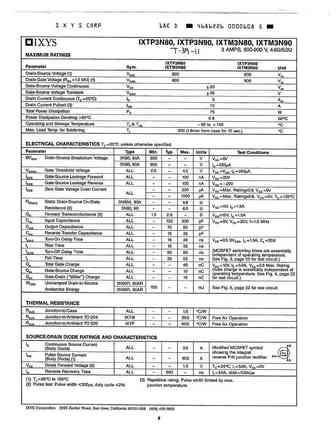
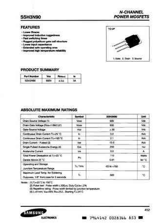
3N90 даташит
3n90.pdf
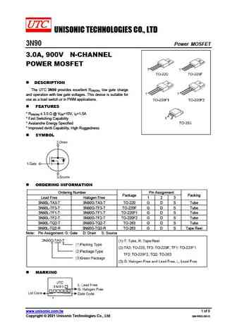
UNISONIC TECHNOLOGIES CO., LTD 3N90 Power MOSFET 3.0A, 900V N-CHANNEL POWER MOSFET DESCRIPTION The UTC 3N90 provides excellent RDS(ON), low gate charge and operation with low gate voltages. This device is suitable for use as a load switch or in PWM applications. FEATURES * RDS(ON) 3.5 @ VGS=10V, ID=1.5A * Fast Switching Capability * Avalanche Energy Spec
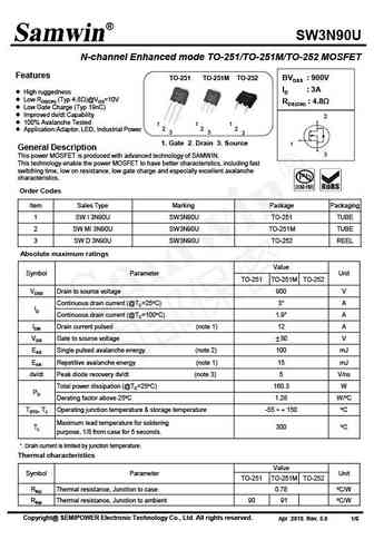
sw3n90u swi3n90u swmi3n90u swd3n90u.pdf
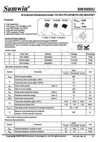
SW3N90U N-channel Enhanced mode TO-251/TO-251M/TO-252 MOSFET Features TO-251 TO-251M TO-252 BVDSS 900V ID 3A High ruggedness Low RDS(ON) (Typ 4.8 )@VGS=10V RDS(ON) 4.8 Low Gate Charge (Typ 19nC) Improved dv/dt Capability 2 100% Avalanche Tested 1 1 1 2 2 2 Application Adaptor, LED, Industrial Power 3 3 3 1. Gate 2. Drain 3. Sou
ssp3n90.pdf
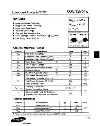
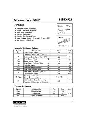
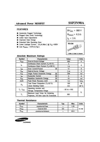
SSP3N90A Advanced Power MOSFET FEATURES BVDSS = 900 V Avalanche Rugged Technology RDS(on) = 6.2 Rugged Gate Oxide Technology Lower Input Capacitance ID = 3 A Improved Gate Charge Extended Safe Operating Area TO-220 Lower Leakage Current 25 A (Max.) @ VDS = 900V Low RDS(ON) 4.679 (Typ.) 1 2 3 1.Gate 2. Drain 3. Source Absolute Maximum Ratings Symbol Chara
fqpf3n90.pdf
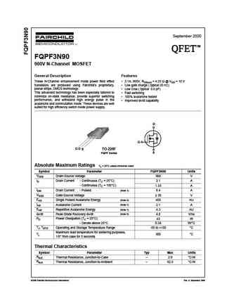
September 2000 TM QFET QFET QFET QFET FQPF3N90 900V N-Channel MOSFET General Description Features These N-Channel enhancement mode power field effect 2.1A, 900V, RDS(on) = 4.25 @ VGS = 10 V transistors are produced using Fairchild s proprietary, Low gate charge ( typical 20 nC) planar stripe, DMOS technology. Low Crss ( typical 8.0 pF) This advanced technology has
fqb3n90tm fqi3n90tu.pdf
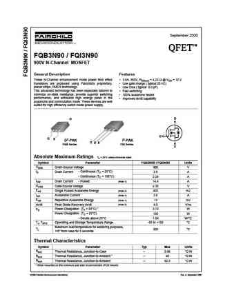
September 2000 TM QFET QFET QFET QFET FQB3N90 / FQI3N90 900V N-Channel MOSFET General Description Features These N-Channel enhancement mode power field effect 3.6A, 900V, RDS(on) = 4.25 @ VGS = 10 V transistors are produced using Fairchild s proprietary, Low gate charge ( typical 20 nC) planar stripe, DMOS technology. Low Crss ( typical 8.0 pF) This advanced techn
fqp3n90.pdf
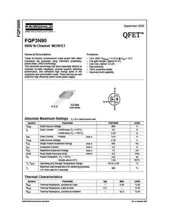
September 2000 TM QFET QFET QFET QFET FQP3N90 900V N-Channel MOSFET General Description Features These N-Channel enhancement mode power field effect 3.6A, 900V, RDS(on) = 4.25 @ VGS = 10 V transistors are produced using Fairchild s proprietary, Low gate charge ( typical 20 nC) planar stripe, DMOS technology. Low Crss ( typical 8.0 pF) This advanced technology has
fqb3n90 fqi3n90.pdf
September 2000 TM QFET QFET QFET QFET FQB3N90 / FQI3N90 900V N-Channel MOSFET General Description Features These N-Channel enhancement mode power field effect 3.6A, 900V, RDS(on) = 4.25 @ VGS = 10 V transistors are produced using Fairchild s proprietary, Low gate charge ( typical 20 nC) planar stripe, DMOS technology. Low Crss ( typical 8.0 pF) This advanced techn
sss3n90a.pdf
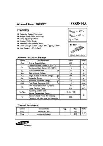
Advanced Power MOSFET FEATURES BVDSS = 900 V Avalanche Rugged Technology RDS(on) = 6.2 Rugged Gate Oxide Technology Lower Input Capacitance ID = 2 A Improved Gate Charge Extended Safe Operating Area Lower Leakage Current 25 A (Max.) @ VDS = 900V Low RDS(ON) 4.679 (Typ.) 1 2 3 1.Gate 2. Drain 3. Source Absolute Maximum Ratings Symbol Characteristic Value
ssp3n90a.pdf
Advanced Power MOSFET FEATURES BVDSS = 900 V Avalanche Rugged Technology RDS(on) = 6.2 Rugged Gate Oxide Technology Lower Input Capacitance ID = 3 A Improved Gate Charge Extended Safe Operating Area Lower Leakage Current 25 A (Max.) @ VDS = 900V Low RDS(ON) 4.679 (Typ.) 1 2 3 1.Gate 2. Drain 3. Source Absolute Maximum Ratings Symbol Characteristic Value
ssw3n90a.pdf
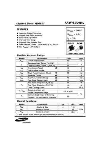
Advanced Power MOSFET FEATURES BVDSS = 900 V Avalanche Rugged Technology RDS(on) = 6.2 Rugged Gate Oxide Technology Lower Input Capacitance ID = 3 A Improved Gate Charge Extended Safe Operating Area Lower Leakage Current 25 A (Max.) @ VDS = 900V 2 Low RDS(ON) 4.679 (Typ.) 1 1 2 3 3 1. Gate 2. Drain 3. Source Absolute Maximum Ratings Symbol Charact
ssu3n90a.pdf
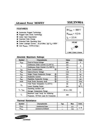
Advanced Power MOSFET FEATURES BVDSS = 900 V Avalanche Rugged Technology RDS(on) = 6.2 Rugged Gate Oxide Technology Lower Input Capacitance ID = 2.5 A Improved Gate Charge Extended Safe Operating Area Lower Leakage Current 25 A (Max.) @ VDS = 900V Low RDS(ON) 4.679 (Typ.) 1 2 3 1. Gate 2. Drain 3. Source Absolute Maximum Ratings Symbol Characteristic Val
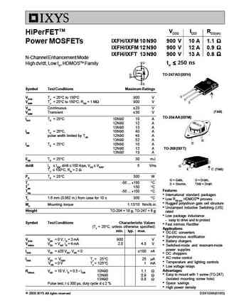
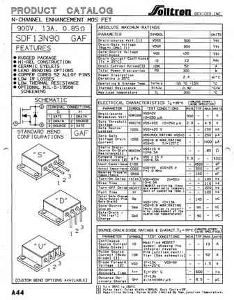
ixfh10n90 ixfm10n90 ixfh12n90 ixfm12n90 ixfh13n90 ixfm13n90.pdf
VDSS ID25 RDS(on) HiPerFETTM IXFH/IXFM 10 N90 900 V 10 A 1.1 Power MOSFETs IXFH/IXFM 12 N90 900 V 12 A 0.9 IXFH/IXFT 13 N90 900 V 13 A 0.8 N-Channel Enhancement Mode 250 ns High dv/dt, Low trr, HDMOSTM Family trr TO-247 AD (IXFH) Symbol Test Conditions Maximum Ratings VDSS TJ = 25 C to 1
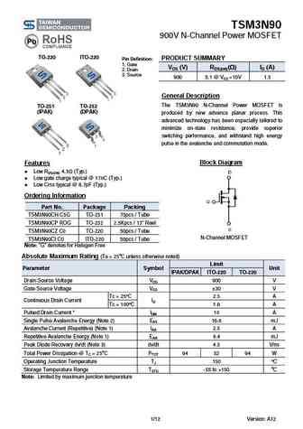
tsm3n90ch tsm3n90ci tsm3n90cp tsm3n90cz.pdf
TSM3N90 900V N-Channel Power MOSFET TO-220 ITO-220 PRODUCT SUMMARY Pin Definition 1. Gate VDS (V) RDS(on)( ) ID (A) 2. Drain 3. Source 900 5.1 @ VGS =10V 1.5 General Description The TSM3N90 N-Channel Power MOSFET is TO-251 TO-252 (IPAK) (DPAK) produced by new advance planar process. This advanced technology has been especially tailored to minimize on-state re
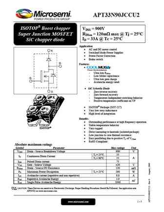
apt33n90jccu2.pdf
APT33N90JCCU2 ISOTOP Boost chopper VDSS = 900V RDSon = 120m max @ Tj = 25 C Super Junction MOSFET ID = 33A @ Tc = 25 C SiC chopper diode Application AC and DC motor control K Switched Mode Power Supplies Power Factor Correction Brake switch D Features - Ultra low RDSon - Low Miller capacitance G - Ultra low gate charge - Avalanche
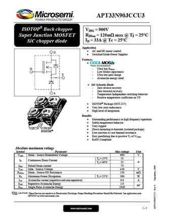
apt33n90jccu3.pdf
APT33N90JCCU3 ISOTOP Buck chopper VDSS = 900V RDSon = 120m max @ Tj = 25 C Super Junction MOSFET ID = 33A @ Tc = 25 C SiC chopper diode Application AC and DC motor control D Switched Mode Power Supplies Features - Ultra low RDSon G - Low Miller capacitance S - Ultra low gate charge - Avalanche energy rated SiC Schottky Diode - Zero rev
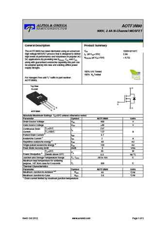
aotf3n90.pdf
AOTF3N90 900V, 2.4A N-Channel MOSFET General Description Product Summary VDS 1000V@150 The AOTF3N90 has been fabricated using an advanced high voltage MOSFET process that is designed to deliver ID (at VGS=10V) 2.4A high levels of performance and robustness in popular AC- RDS(ON) (at VGS=10V)
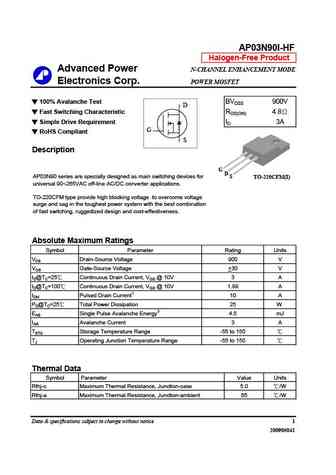
ap03n90i-hf.pdf
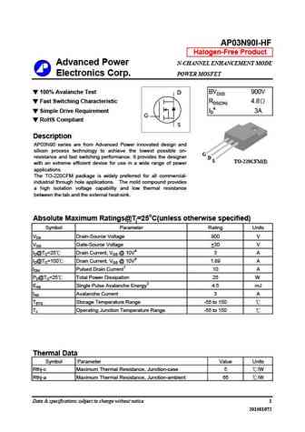
AP03N90I-HF Halogen-Free Product Advanced Power N-CHANNEL ENHANCEMENT MODE Electronics Corp. POWER MOSFET 100% Avalanche Test BVDSS 900V D Fast Switching Characteristic RDS(ON) 4.8 Simple Drive Requirement ID 3A G RoHS Compliant S Description G D AP03N90 series are specially designed as main switching devices for S TO-220CFM(I) universal 90 265VAC off-line AC/D
ap03n90p-hf.pdf
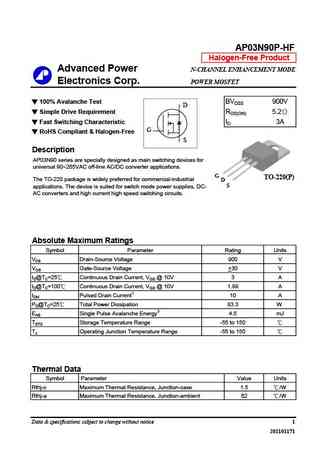
AP03N90P-HF Halogen-Free Product Advanced Power N-CHANNEL ENHANCEMENT MODE Electronics Corp. POWER MOSFET 100% Avalanche Test BVDSS 900V D Simple Drive Requirement RDS(ON) 5.2 Fast Switching Characteristic ID 3A G RoHS Compliant & Halogen-Free S Description AP03N90 series are specially designed as main switching devices for universal 90 265VAC off-line AC/DC conve
ap03n90i.pdf
AP03N90I-HF Halogen-Free Product Advanced Power N-CHANNEL ENHANCEMENT MODE Electronics Corp. POWER MOSFET 100% Avalanche Test BVDSS 900V D Fast Switching Characteristic RDS(ON) 4.8 Simple Drive Requirement ID4 3A G RoHS Compliant S Description AP03N90 series are from Advanced Power innovated design and silicon process technology to achieve the lowest possible on-
jcs13n90aba jcs13n90wa.pdf
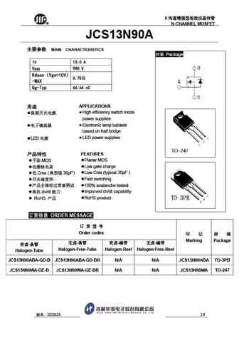
N R N-CHANNEL MOSFET JCS13N90A MAIN CHARACTERISTICS Package ID 13.0 A VDSS 900 V Rdson Vgs=10V 0.75 -MAX Qg-Typ 66.64 nC APPLICATIONS High efficiency switch mode . power supplies Electronic lamp ballasts based on half bridge LED power s
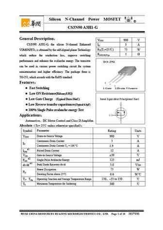
cs3n90 a3h.pdf
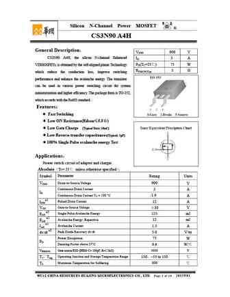
Silicon N-Channel Power MOSFET R CS3N90 A3H General Description VDSS 900 V CS3N90 A3H, the silicon N-channel Enhanced ID 3 A PD(TC=25 ) 75 W VDMOSFETs, is obtained by the self-aligned planar Technology RDS(ON)Typ 5 which reduce the conduction loss, improve switching performance and enhance the avalanche energy. The transistor can be used in various power swit
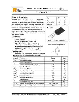
cs3n90f a9h.pdf
Silicon N-Channel Power MOSFET R CS3N90F A9H General Description VDSS 900 V CS3N90F A9H, the silicon N-channel Enhanced VDMOSFET, ID 3 A PD(TC=25 ) 30 W is obtained by the self-aligned planar Technology which reduce RDS(ON)Typ 4.7 the conduction loss, improve switching performance and enhance the avalanche energy. The transistor can be used in various powe
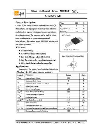
cs3n90 a8.pdf
Silicon N-Channel Power MOSFET R CS3N90 A8 General Description VDSS 900 V CS3N90 A8, the silicon N-channel Enhanced VDMOSFETs, is ID 3 A PD(TC=25 ) 80 W obtained by the self-aligned planar Technology which reduce the RDS(ON)Typ 5.0 conduction loss, improve switching performance and enhance the avalanche energy. The transistor can be used in various power swi
cs3n90 a4h.pdf
Silicon N-Channel Power MOSFET R CS3N90 A4H General Description VDSS 900 V CS3N90 A4H, the silicon N-channel Enhanced ID 3 A PD(TC=25 ) 75 W VDMOSFETs, is obtained by the self-aligned planar Technology RDS(ON)Typ 5 which reduce the conduction loss, improve switching performance and enhance the avalanche energy. The transistor can be used in various power sw
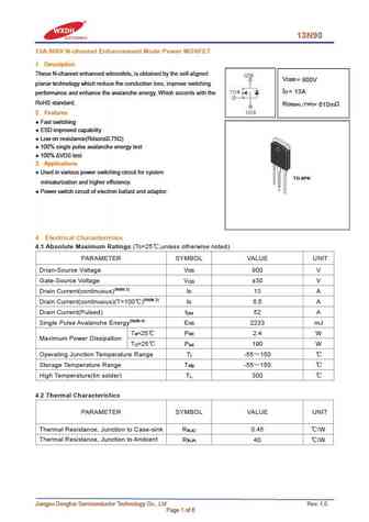
13n90.pdf
13N90 13A 900V N-channel Enhancement Mode Power MOSFET 1 Description These N-channel enhanced vdmosfets, is obtained by the self-aligned V DSS = 900V planar technology which reduce the conduction loss, improve switching I = 13A D performance and enhance the avalanche energy. Which accords with the RoHS standard. R DS(on) TYP) = 610m 2 Features Fast switching ESD impr
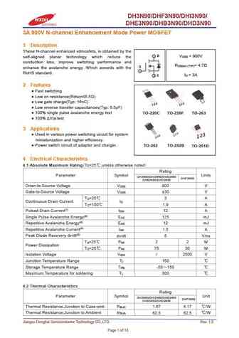
dh3n90 dhf3n90 dhi3n90 dhe3n90 dhb3n90 dhd3n90.pdf
DH3N90/DHF3N90/DHI3N90/ DHE3N90/DHB3N90/DHD3N90 3A 900V N-channel Enhancement Mode Power MOSFET 1 Description These N-channel enhanced vdmosfets, is obtained by the 2 D V = 900V DSS self-aligned planar technology which reduce the conduction loss, improve switching performance and R = 4.7 DS(on) (TYP) G enhance the avalanche energy. Which accords with the 1 RoHS standard. I = 3
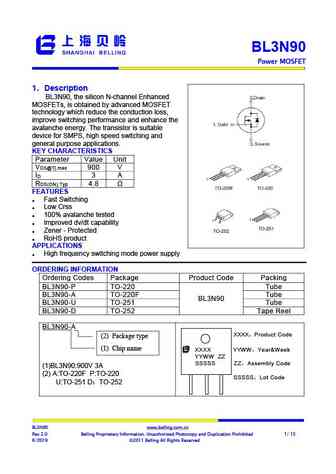
bl3n90-p bl3n90-a bl3n90-u bl3n90-d.pdf
BL3N90 Power MOSFET 1 Description Step-Down Converter BL3N90, the silicon N-channel Enhanced , MOSFETs, is obtained by advanced MOSFET technology which reduce the conduction loss, improve switching performance and enhance the avalanche energy. The transistor is suitable device for SMPS, high speed switching and general purpose applications. KEY CHARACTERISTICS Param
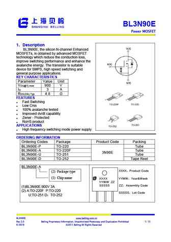
bl3n90e-p bl3n90e-a bl3n90e-u bl3n90e-d.pdf
BL3N90E Power MOSFET 1 Description Step-Down Converter BL3N90E, the silicon N-channel Enhanced , MOSFETs, is obtained by advanced MOSFET technology which reduce the conduction loss, improve switching performance and enhance the avalanche energy. The transistor is suitable device for SMPS, high speed switching and general purpose applications. KEY CHARACTERISTICS Par
swi3n90u swmi3n90u swd3n90u.pdf
SW3N90U N-channel Enhanced mode TO-251/TO-251M/TO-252 MOSFET Features TO-251 TO-251M TO-252 BVDSS 900V ID 3A High ruggedness Low RDS(ON) (Typ 4.8 )@VGS=10V RDS(ON) 4.8 Low Gate Charge (Typ 19nC) Improved dv/dt Capability 2 100% Avalanche Tested 1 1 1 2 2 2 Application Adaptor, LED, Industrial Power 3 3 3 1. Gate 2. Drain 3. Sou
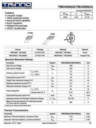
tmd3n90 tmu3n90.pdf
TMD3N90(G)/TMU3N90(G) N-channel MOSFET Features BVDSS ID RDS(on) Low gate charge 900V 2.5A
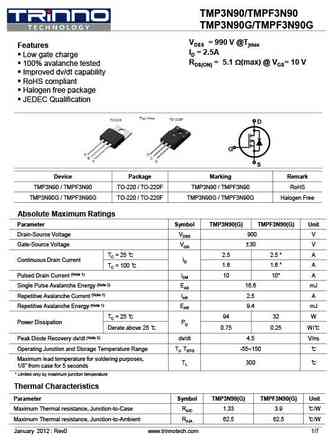
tmp3n90 tmpf3n90.pdf
TMP3N90/TMPF3N90 TMP3N90G/TMPF3N90G VDSS = 990 V @Tjmax Features ID = 2.5A Low gate charge RDS(ON) = 5.1 W(max) @ VGS= 10 V 100% avalanche tested Improved dv/dt capability RoHS compliant Halogen free package JEDEC Qualification D G S Device Package Marking Remark TMP3N90 / TMPF3N90 TO-220 / TO-220F TMP3N90 / TMPF3N90 RoHS TMP3N90G / TMPF
cs3n90fa9h.pdf
Silicon N-Channel Power MOSFET R CS3N90F A9H General Description VDSS 900 V CS3N90F A9H, the silicon N-channel Enhanced VDMOSFET, ID 3 A PD(TC=25 ) 30 W is obtained by the self-aligned planar Technology which reduce RDS(ON)Typ 4.7 the conduction loss, improve switching performance and enhance the avalanche energy. The transistor can be used in various powe
cs3n90a3h1-g.pdf
Silicon N-Channel Power MOSFET R CS3N90 A3H1-G General Description VDSS 900 V CS3N90 A3H1-G, the silicon N-channel Enhanced ID 3 A PD(TC=25 ) 75 W VDMOSFETs, is obtained by the self-aligned planar Technology RDS(ON)Typ 5 which reduce the conduction loss, improve switching performance and enhance the avalanche energy. The transistor can be used in various po
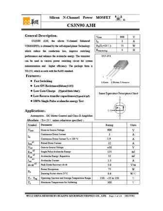
cs3n90a3h.pdf
Silicon N-Channel Power MOSFET R CS3N90 A3H General Description VDSS 900 V CS3N90 A3H, the silicon N-channel Enhanced ID 3 A PD(TC=25 ) 75 W VDMOSFETs, is obtained by the self-aligned planar Technology RDS(ON)Typ 5 which reduce the conduction loss, improve switching performance and enhance the avalanche energy. The transistor can be used in various power swit
cs3n90a4h.pdf
Silicon N-Channel Power MOSFET R CS3N90 A4H General Description VDSS 900 V CS3N90 A4H, the silicon N-channel Enhanced ID 3 A PD(TC=25 ) 75 W VDMOSFETs, is obtained by the self-aligned planar Technology RDS(ON)Typ 5 which reduce the conduction loss, improve switching performance and enhance the avalanche energy. The transistor can be used in various power sw
cs3n90a8.pdf
Silicon N-Channel Power MOSFET R CS3N90 A8 General Description VDSS 900 V CS3N90 A8, the silicon N-channel Enhanced VDMOSFETs, is ID 3 A PD(TC=25 ) 80 W obtained by the self-aligned planar Technology which reduce the RDS(ON)Typ 5.0 conduction loss, improve switching performance and enhance the avalanche energy. The transistor can be used in various power swi
cs3n90f cs3n90p cs3n90b.pdf
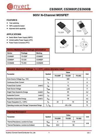
nvert Suzhou Convert Semiconductor Co ., Ltd. CS3N90F, CS3N90P,CS3N90B 900V N-Channel MOSFET FEATURES Fast switching 100% avalanche tested Improved dv/dt capability APPLICATIONS Switch Mode Power Supply (SMPS) Uninterruptible Power Supply (UPS) Power Factor Correction (PFC) Device Marking and Package Information Device Package Marking CS3N90F TO-220F CS3N90
hm3n90f.pdf
HM3N90F Silicon N-Channel Power MOSFET General Description VDSS 900 V HM3N90F, the silicon N-channel Enhanced VDMOSFET, ID 3 A PD(TC=25 ) 30 W is obtained by the self-aligned planar Technology which reduce RDS(ON)Typ 4.7 the conduction loss, improve switching performance and enhance the avalanche energy. The transistor can be used in various power switching circuit
hm3n90i.pdf
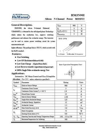
HM3N90I Silicon N-Channel Power MOSFET General Description VDSS 900 V HM3N90I, the silicon N-channel Enhanced ID 3 A PD(TC=25 ) 75 W VDMOSFETs, is obtained by the self-aligned planar Technology RDS(ON)Typ 5 which reduce the conduction loss, improve switching performance and enhance the avalanche energy. The transistor can be used in various power switching circuit for
aotf3n90.pdf
isc N-Channel MOSFET Transistor AOTF3N90 FEATURES Drain Current I =2.4A@ T =25 D C Drain Source Voltage- V =900V(Min) DSS Static Drain-Source On-Resistance R =6.7 (Max) DS(on) 100% avalanche tested Minimum Lot-to-Lot variations for robust device performance and reliable operation DESCRIPTION Designed for use in switch mode power supplies and general purpose
sw3n90u.pdf
isc N-Channel MOSFET Transistor SW3N90U FEATURES Drain Current I = 3.0A@ T =25 D C Drain Source Voltage V = 900V(Min) DSS Static Drain-Source On-Resistance R = 5.8 (Max) @ V = 10V DS(on) GS 100% avalanche tested Minimum Lot-to-Lot variations for robust device performance and reliable operation DESCRIPTION motor drive, DC-DC converter, power switch and soleno
Другие MOSFET... 9N90 , 10N90 , 11N90 , 12N90 , 9N95 , 9N100 , 1N90 , 2N90 , AON6414A , 4N90 , 5N90 , 6N90 , 7N90 , 1N80 , 2N80 , 3N80 , 4N80 .
🌐 : EN ES РУ
Список транзисторов
Обновления
MOSFET: ASD80R750E | ASD70R950E | ASD70R600E | ASD70R380E | ASD65R850E | ASD65R550E | ASD65R350E | ASD65R300E | ASD65R280E | ASD65R270E | ASD60R330E | ASD60R280E | ASB80R750E | ASB70R380E | ASB65R300E | ASB65R220E
Popular searches
tip127 datasheet | irlz24n | irf620 | irfp350 | 13003 transistor | c458 transistor | 2sc1775 | 2n1305
