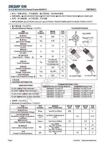
7N65. Аналоги и основные параметры
Наименование производителя: 7N65
Тип транзистора: MOSFET
Полярность: N
Предельные значения
Pd ⓘ - Максимальная рассеиваемая мощность: 142 W
|Vds|ⓘ - Максимально допустимое напряжение сток-исток: 650 V
|Vgs|ⓘ - Максимально допустимое напряжение затвор-исток: 30 V
|Id| ⓘ - Максимально допустимый постоянный ток стока: 7.4 A
Tj ⓘ - Максимальная температура канала: 150 °C
Электрические характеристики
tr ⓘ - Время нарастания: 150 ns
Cossⓘ - Выходная емкость: 140 pf
RDSonⓘ - Сопротивление сток-исток открытого транзистора: 0.94 Ohm
Тип корпуса: TO-220 TO-262 TO-263 TO-220F TO-220F1 TO-220F2
Аналог (замена) для 7N65
- подборⓘ MOSFET транзистора по параметрам
7N65 даташит
7n65.pdf

UNISONIC TECHNOLOGIES CO., LTD 7N65 Power MOSFET 7.4A, 650V N-CHANNEL POWER MOSFET DESCRIPTION The UTC 7N65 is a high voltage power MOSFET and is designed to have better characteristics, such as fast switching time, low gate charge, low on-state resistance and have a high rugged avalanche characteristics. This power MOSFET is usually used at high speed switching applicatio
7n65.pdf
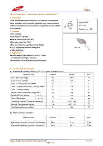
7N65 7A 650V N-channel Enhancement Mode Power MOSFET 1 Description These N-channel enhanced vdmosfets, is obtained by the self-aligned V DSS = 650V planar technology which reduce the conduction loss, improve switching I = 7.0A D performance and enhance the avalanche energy. Which accords with the RoHS standard. R DS(on) TYP) =1.2 2 Features Fast switching ESD improve
7n65.pdf
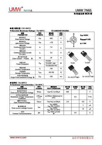
R UMW UMW 7N65 UMW 7N65 N- MOS N- MOS N- MOS N- MOS TC=25 C TC=25 TC=25 C TC=25 C C Absolute Maximum Ratings Tc=25 C TO-220/220F/262/263 /220F/262/263 /220F/262/263 /220F/262/263 Absolute Maximum Ratings Tc=25 C TO-220/220F/262/263 Absolute Maximum Ratings Tc=25 C TO-220 Absolute Maximum Ratings T
7n65.pdf
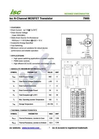
INCHANGE Semiconductor isc N-Channel MOSFET Transistor 7N65 FEATURES Drain Current I = 7A@ T =25 D C Drain Source Voltage V = 650V(Min) DSS Static Drain-Source On-Resistance RDS(on) = 1.35 (Max) @VGS = 10 V Avalanche Energy Specified Fast Switching Minimum Lot-to-Lot variations for robust device performance and reliable operation APPLICATIONS High speed
fcpf067n65s3.pdf

Is Now Part of To learn more about ON Semiconductor, please visit our website at www.onsemi.com ON Semiconductor and the ON Semiconductor logo are trademarks of Semiconductor Components Industries, LLC dba ON Semiconductor or its subsidiaries in the United States and/or other countries. ON Semiconductor owns the rights to a number of patents, trademarks, copyrights, trade secrets, and oth
utc7n65l.pdf
UNISONIC TECHNOLOGIES CO., LTD 7N65 Power MOSFET 7.4A, 650V N-CHANNEL POWER MOSFET DESCRIPTION The UTC 7N65 is a high voltage power MOSFET and is designed to have better characteristics, such as fast switching time, low gate charge, low on-state resistance and have a high rugged avalanche characteristics. This power MOSFET is usually used at high speed switching applications
std7n65m2.pdf
STD7N65M2 N-channel 650 V, 0.98 typ., 5 A MDmesh M2 Power MOSFET in a DPAK package Datasheet - production data Features RDS(on) Order code VDS max ID TAB STD7N65M2 650 V 1.15 5 A 3 Extremely low gate charge 1 Excellent output capacitance (Coss) profile 100% avalanche tested DPAK Zener-protected Applications Switching applications Figure 1. Inte
stp7n65m2 stu7n65m2.pdf
STP7N65M2, STU7N65M2 N-channel 650 V, 0.98 typ., 5 A MDmesh M2 Power MOSFETs in TO-220 and IPAK packages Datasheet - production data Features TAB R DS(on) Order code VDS ID max STP7N65M2 650 V 1.15 5 A 3 2 STU7N65M2 650 V 1.15 5 A TAB 1 TO-220 Extremely low gate charge 3 2 Excellent output capacitance (Coss) profile IPAK 1 100% avalanche
stw57n65m5-4.pdf
STW57N65M5-4 N-channel 650 V, 0.056 typ., 42 A, MDmesh V Power MOSFET in a TO247-4 package Datasheet - production data Features RDS(on) Order code VDS @ TJmax max ID STW57N65M5-4 710 V 0.063 42 A Higher VDS rating 4 Higher dv/dt capability 3 2 1 Excellent switching performance thanks to the extra driving source pin TO247-4 Easy to drive 100% aval
stf7n65m2.pdf
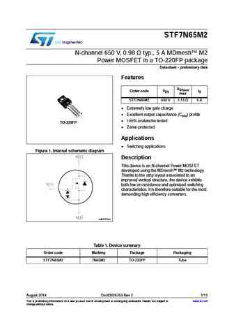
STF7N65M2 N-channel 650 V, 0.98 typ., 5 A MDmesh M2 Power MOSFET in a TO-220FP package Datasheet - preliminary data Features RDS(on) Order code VDS max ID STF7N65M2 650 V 1.15 5 A Extremely low gate charge 3 2 Excellent output capacitance (Coss) profile 1 100% avalanche tested TO-220FP Zener-protected Applications Switching applications Figure 1
stl57n65m5.pdf
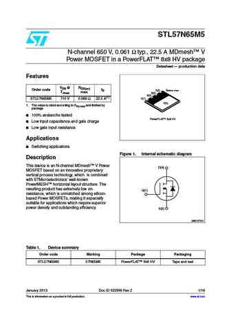
STL57N65M5 N-channel 650 V, 0.061 typ., 22.5 A MDmesh V Power MOSFET in a PowerFLAT 8x8 HV package Datasheet production data Features VDS @ RDS(on) Order code ID S(2) Bottom view TJmax max S(2) S(2) G(1) STL57N65M5 710 V 0.069 22.5 A(1) D(3) 1. The value is rated according to Rthj-case and limited by package 100% avalanche tested PowerFLAT 8x8 HV
stl17n65m5.pdf
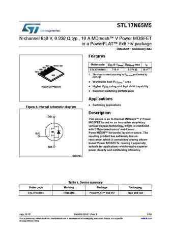
STL17N65M5 N-channel 650 V, 0.338 typ., 10 A MDmesh V Power MOSFET in a PowerFLAT 8x8 HV package Datasheet - preliminary data Features Order code VDS @ TJmax RDS(on) max ID S(2) Bottom view S(2) S(2) STL17N65M5 710 V 0.374 10 A(1) G(1) 1. The value is rated according to Rthj-case and limited by D(3) package Worldwide best RDS(on) * area Higher VDSS rating an
stw57n65m5 stwa57n65m5.pdf
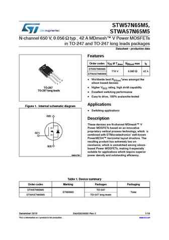
STW57N65M5, STWA57N65M5 N-channel 650 V, 0.056 typ., 42 A MDmesh V Power MOSFETs in TO-247 and TO-247 long leads packages Datasheet - production data Features Order codes VDS @ TJmax RDS(on) max ID STW57N65M5 710 V 0.063 42 A STWA57N65M5 Worldwide best RDS(on)*area amongst the 3 2 silicon based devices 1 TO-247 Higher VDSS rating, high dv/dt capability TO-24
stw77n65m5.pdf
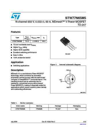
STW77N65M5 N-channel 650 V, 0.033 , 69 A, MDmesh V Power MOSFET TO-247 Features VDSS Type RDS(on) max ID @TjMAX STW77N65M5 710 V
stb57n65m5 stf57n65m5 sti57n65m5 stp57n65m5.pdf
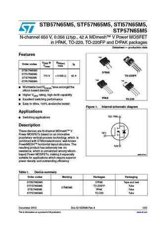
STB57N65M5, STF57N65M5, STI57N65M5, STP57N65M5 N-channel 650 V, 0.056 typ., 42 A MDmesh V Power MOSFET in I PAK, TO-220, TO-220FP and D PAK packages Datasheet production data Features TAB VDSS @ RDS(on) Order codes ID TJmax max 3 1 3 STB57N65M5 2 1 D PAK STF57N65M5 710 V
tk17n65w.pdf
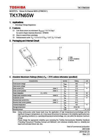
TK17N65W MOSFETs Silicon N-Channel MOS (DTMOS ) TK17N65W TK17N65W TK17N65W TK17N65W 1. Applications 1. Applications 1. Applications 1. Applications Switching Voltage Regulators 2. Features 2. Features 2. Features 2. Features (1) Low drain-source on-resistance RDS(ON) = 0.17 (typ.) by used to Super Junction Structure DTMOS (2) Easy to control Gate switching (3) En
fqb7n65ctm.pdf
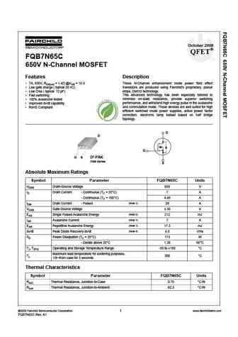
October 2008 QFET FQB7N65C 650V N-Channel MOSFET Features Description 7A, 650V, RDS(on) = 1.4 @VGS = 10 V These N-Channel enhancement mode power field effect Low gate charge ( typical 28 nC) transistors are produced using Fairchild s proprietary, planar stripe, DMOS technology. Low Crss ( typical 12 pF) This advanced technology has been especially tailored to Fa
fqp7n65c fqpf7n65c.pdf

QFET FQP7N65C/FQPF7N65C 650V N-Channel MOSFET General Description Features These N-Channel enhancement mode power field effect 7A, 650V, RDS(on) = 1.4 @VGS = 10 V transistors are produced using Fairchild s proprietary, Low gate charge ( typical 28 nC) planar stripe, DMOS technology. Low Crss ( typical 12 pF) This advanced technology has been especially tailored to
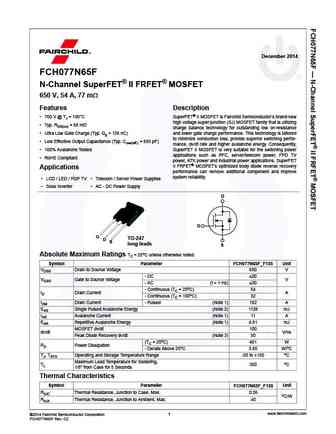
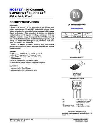
fch077n65f f085.pdf
December 2014 FCH077N65F_F085 N-Channel SuperFET II FRFET MOSFET 650 V, 54 A, 77 m D Features Typical RDS(on) = 68 m at VGS = 10 V, ID = 27 A Typical Qg(tot) = 126 nC at VGS = 10V, ID = 27 A UIS Capability G Qualified to AEC Q101 G RoHS Compliant D TO-247 S S Description SuperFET II MOSFET is Fairchild Semiconductor s brand-new For current package drawing
fqp7n65c fqpf7n65cydtu fqpf7n65c f105.pdf
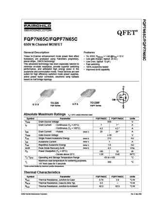
QFET FQP7N65C/FQPF7N65C 650V N-Channel MOSFET General Description Features These N-Channel enhancement mode power field effect 7A, 650V, RDS(on) = 1.4 @VGS = 10 V transistors are produced using Fairchild s proprietary, Low gate charge ( typical 28 nC) planar stripe, DMOS technology. Low Crss ( typical 12 pF) This advanced technology has been especially tailored to
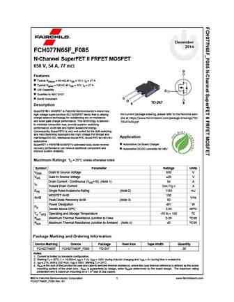
fch077n65f.pdf
December 2014 FCH077N65F N-Channel SuperFET II FRFET MOSFET 650 V, 54 A, 77 m Features Description 700 V @ TJ = 150 C SuperFET II MOSFET is Fairchild Semiconductor s brand-new high voltage super-junction (SJ) MOSFET family that is utilizing Typ. RDS(on) = 68 m charge balance technology for outstanding low on-resistance Ultra Low Gate Charge (Typ. Qg = 126 nC
sihg47n65e.pdf
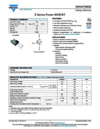
SiHG47N65E www.vishay.com Vishay Siliconix E Series Power MOSFET FEATURES PRODUCT SUMMARY Low figure-of-merit (FOM) Ron x Qg VDS (V) at TJ max. 700 Low input capacitance (Ciss) RDS(on) max. at 25 C ( ) VGS = 10 V 0.072 Reduced switching and conduction losses Qg max. (nC) 273 Ultra low gate charge (Qg) Qgs (nC) 46 Qgd (nC) 79 Avalanche energy rated (UIS) Co
dmg7n65sj3.pdf
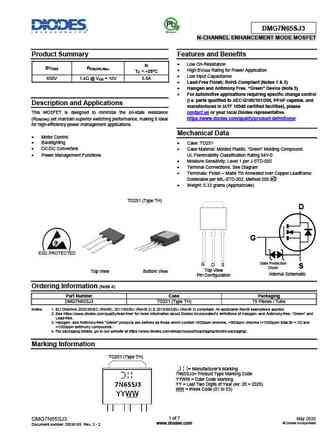
DMG7N65SJ3 N-CHANNEL ENHANCEMENT MODE MOSFET Product Summary Features and Benefits Low On-Resistance I D BV R DSS DS(ON) Max High BV Rating for Power Application DSS T = +25 C C Low Input Capacitance 650V 1.4 @ V = 10V 5.5A GS Lead-Free Finish; RoHS Compliant (Notes 1 & 2) Halogen and Antimony Free. Green Device (Note 3) For automot
dmg7n65scti.pdf
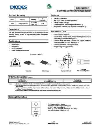
DMG7N65SCTI N-CHANNEL ENHANCEMENT MODE MOSFET Product Summary Features Low Input Capacitance ID BVDSS RDS(ON) Package TC = +25 High BVDSS Rating for Power Application C ITO220AB Low Input/Output Leakage 650V 1.4 @VGS = 10V 7.7A (Type TH) Lead-Free Finish; RoHS Compliant (Notes 1 & 2) Halogen and Antimony Free. Green Device (Note 3) Descrip
dmg7n65sct.pdf
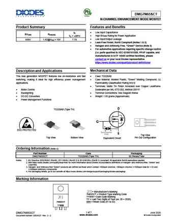
DMG7N65SCT N-CHANNEL ENHANCEMENT MODE MOSFET Product Summary Features and Benefits Low Input Capacitance I D BV R DSS DS(ON) High BV Rating for Power Application DSS T = +25 C C Low Input/Output Leakage 650V 1.4 @V = 10V 7.7A GS Lead-Free Finish; RoHS Compliant (Notes 1 & 2) Halogen and Antimony Free. Green Device (Note 3) For automo
spp07n65c3 spa07n65c3 spi07n65c3 rev1.92.pdf
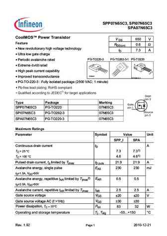
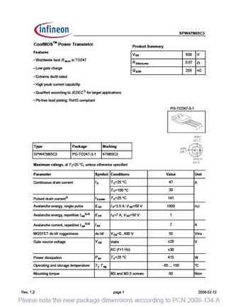
SPP07N65C3, SPI07N65C3 SPA07N65C3 CoolMOS Power Transistor V 650 V DS Feature RDS(on) 0.6 New revolutionary high voltage technology ID 7.3 A Ultra low gate charge PG-TO220-3 PG-TO262-3-1 PG-TO220 Periodic avalanche rated 2 Extreme dv/dt rated 3 High peak current capability 2 3 2 1 1 P-TO220-3-31 Improved transconductance P-TO220-3-1 PG-TO
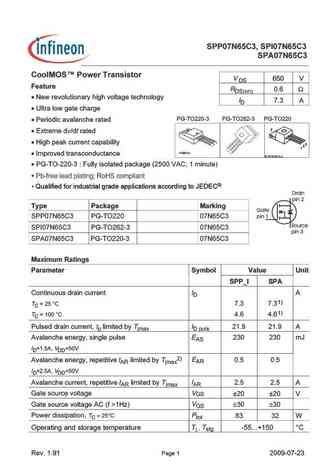
spw47n65c3.pdf
SPW47N65C3 CoolMOSTM Power Transistor Product Summary Features V 650 V DS Worldwide best R in TO247 ds,on R 0.07 DS(on),max Low gate charge Q 255 nC g,typ Extreme dv/dt rated High peak current capability Qualified according to JEDEC1) for target applications Pb-free lead plating; RoHS compliant PG-TO247-3-1 Type Package Marking SPW47N65C3 PG-TO247
mcp07n65.pdf
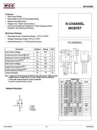
MCP07N65 Features High Current Rating Epoxy Meets UL 94 V-0 Flammability Rating Moisture Sensitivity Level 1 Halogen Free. Green Device (Note 1) N-CHANNEL Lead Free Finish/RoHS Compliant ("P" Suffix Designates RoHS Compliant. See Ordering Information) MOSFET Maximum Ratings Operating Junction Temperature Range -55 C to +150 C Storage Temperatur
mcpf07n65.pdf
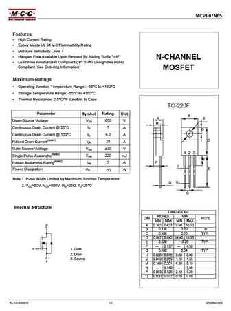
MCPF07N65 Features High Current Rating Epoxy Meets UL 94 V-0 Flammability Rating Moisture Sensitivity Level 1 Halogen Free Available Upon Request By Adding Suffix "-HF" N-CHANNEL Lead Free Finish/RoHS Compliant ("P" Suffix Designates RoHS Compliant. See Ordering Information) MOSFET Maximum Ratings Operating Junction Temperature Range -55 C to +150 C S
fch077n65f-f085.pdf
MOSFET N-Channel, SUPERFET) II, FRFET) 650 V, 54 A, 77 mW FCH077N65F-F085 Description SuperFET II MOSFET is ON Semiconductor s brand-new high www.onsemi.com voltage super-junction (SJ) MOSFET family that is utilizing charge balance technology for outstanding low on-resistance and lower gate charge performance. This technology is tailored to minimize VDS RDS(ON) MAX ID MAX condu
nth4l027n65s3f.pdf
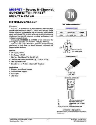
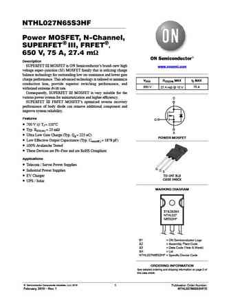
MOSFET Power, N-Channel, SUPERFET) III, FRFET) 650 V, 75 A, 27.4 mW NTH4L027N65S3F Description www.onsemi.com SUPERFET III MOSFET is ON Semiconductor s brand-new high voltage super-junction (SJ) MOSFET family that is utilizing charge balance technology for outstanding low on-resistance and lower gate VDSS RDS(ON) MAX ID MAX charge performance. This advanced technology is tailored
nvhl027n65s3f.pdf
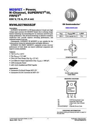
MOSFET Power, N-Channel, SUPERFET) III, FRFET) 650 V, 75 A, 27.4 mW NVHL027N65S3F www.onsemi.com Description SUPERFET III MOSFET is ON Semiconductor s brand-new high voltage super-junction (SJ) MOSFET family that is utilizing charge VDSS RDS(ON) MAX ID MAX balance technology for outstanding low on-resistance and lower gate charge performance. This advanced technology is tailore
fcp067n65s3.pdf
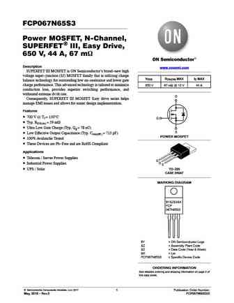
FCP067N65S3 Power MOSFET, N-Channel, SUPERFET) III, Easy Drive, 650 V, 44 A, 67 mW Description www.onsemi.com SUPERFET III MOSFET is ON Semiconductor s brand-new high voltage super-junction (SJ) MOSFET family that is utilizing charge VDSS RDS(ON) MAX ID MAX balance technology for outstanding low on-resistance and lower gate charge performance. This advanced technology is tailored to
fch067n65s3.pdf
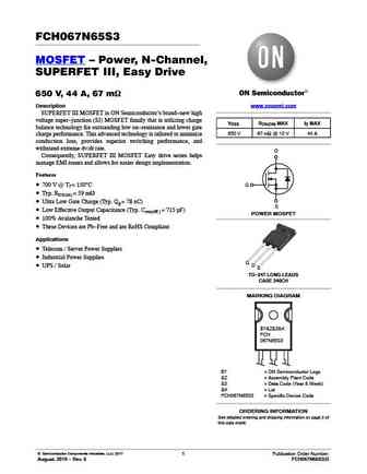
FCH067N65S3 MOSFET Power, N-Channel, SUPERFET III, Easy Drive 650 V, 44 A, 67 mW Description www.onsemi.com SUPERFET III MOSFET is ON Semiconductor s brand-new high voltage super-junction (SJ) MOSFET family that is utilizing charge VDSS RDS(ON) MAX ID MAX balance technology for outstanding low on-resistance and lower gate 650 V 67 mW @ 10 V 44 A charge performance. This advanced
fch077n65f.pdf

Is Now Part of To learn more about ON Semiconductor, please visit our website at www.onsemi.com Please note As part of the Fairchild Semiconductor integration, some of the Fairchild orderable part numbers will need to change in order to meet ON Semiconductor s system requirements. Since the ON Semiconductor product management systems do not have the ability to manage part nomenclatur
nth027n65s3f.pdf
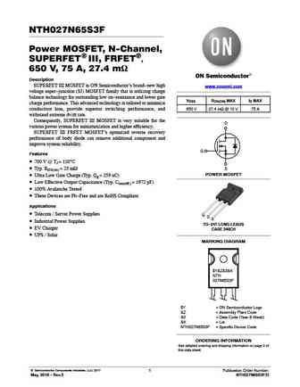
NTH027N65S3F Power MOSFET, N-Channel, SUPERFET) III, FRFET), 650 V, 75 A, 27.4 mW Description SUPERFET III MOSFET is ON Semiconductor s brand-new high www.onsemi.com voltage super-junction (SJ) MOSFET family that is utilizing charge balance technology for outstanding low on-resistance and lower gate VDSS RDS(ON) MAX ID MAX charge performance. This advanced technology is tailored to
nthl027n65s3hf.pdf
NTHL027N65S3HF Power MOSFET, N-Channel, SUPERFET) III, FRFET), 650 V, 75 A, 27.4 mW Description SUPERFET III MOSFET is ON Semiconductor s brand-new high www.onsemi.com voltage super-junction (SJ) MOSFET family that is utilizing charge balance technology for outstanding low on-resistance and lower gate charge performance. This advanced technology is tailored to minimize VDSS RDS(ON)
7n65k.pdf

UNISONIC TECHNOLOGIES CO., LTD 7N65K Preliminary Power MOSFET 7.4A, 650V N-CHANNEL POWER MOSFET DESCRIPTION The UTC 7N65K is a high voltage power MOSFET and is designed to have better characteristics, such as fast switching time, low gate charge, low on-state resistance and have a high rugged avalanche characteristics. This power MOSFET is usually used at high speed switch
7n65a.pdf
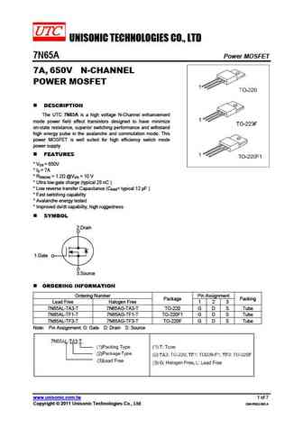
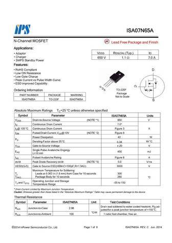
UNISONIC TECHNOLOGIES CO., LTD 7N65A Power MOSFET 7A, 650V N-CHANNEL POWER MOSFET DESCRIPTION The UTC 7N65A is a high voltage N-Channel enhancement mode power field effect transistors designed to have minimize on-state resistance, superior switching performance and withstand high energy pulse in the avalanche and commutation mode. This power MOSFET is well suited for high ef
7n65kl-tm3-t 7n65kg-tm3-t 7n65kl-tn3-r 7n65kg-tn3-r 7n65kg-tf2-t 7n65kl-tf3t-t 7n65kg-tf3t-t.pdf

UNISONIC TECHNOLOGIES CO., LTD 7N65K-MTQ Power MOSFET 7A, 650V N-CHANNEL POWER MOSFET DESCRIPTION The UTC 7N65K-MTQ is a high voltage power MOSFET designed to have better characteristics, such as fast switching time, low gate charge, low on-state resistance and high rugged avalanche characteristics. This power MOSFET is usually used in high speed switching applications of s
7n65l-ta3-t 7n65g-ta3-t 7n65l-tf1-t 7n65g-tf1-t 7n65l-tf3-t 7n65g-tf3-t 7n65l-tf3t-t 7n65g-tf3t-t 7n65l-tm3-t.pdf

UNISONIC TECHNOLOGIES CO., LTD 7N65-TC Power MOSFET 7A, 650V N-CHANNEL POWER MOSFET 1 1 TO-220 TO-220F DESCRIPTION The UTC 7N65-TC is a N-channel mode power MOSFET using 1 UTC s advanced technology to provide customers with planar stripe 1 and DMOS technology. This technology allows a minimum on-state TO-220F3 TO-220F1 resistance and superior switching performance.
7n65kl-ta3-t 7n65kg-ta3-t 7n65kl-tf3-t 7n65kg-tf3-t 7n65kl-tf1-t 7n65kg-tf1-t 7n65kl-tf2-t 7n65kg-tf2-t.pdf

UNISONIC TECHNOLOGIES CO., LTD 7N65K-MTQ Power MOSFET 7.0A, 650V N-CHANNEL POWER MOSFET DESCRIPTION The UTC 7N65K-MTQ is a high voltage power MOSFET designed to have better characteristics, such as fast switching time, low gate charge, low on-state resistance and high rugged avalanche characteristics. This power MOSFET is usually used in high speed switching applications of
7n65l-t2q-t 7n65g-t2q-t 7n65l-tq2-r 7n65g-tq2-r 7n65l-tq2-t 7n65g-tq2-t 7n65g-tf3-t.pdf

UNISONIC TECHNOLOGIES CO., LTD 7N65-R Power MOSFET 7.4A, 650V N-CHANNEL POWER MOSFET DESCRIPTION The UTC 7N65-R is a high voltage power MOSFET and is designed to have better characteristics, such as fast switching time, low gate charge, low on-state resistance and have a high rugged avalanche characteristics. This power MOSFET is usually used at high speed switching applic
7n65z.pdf
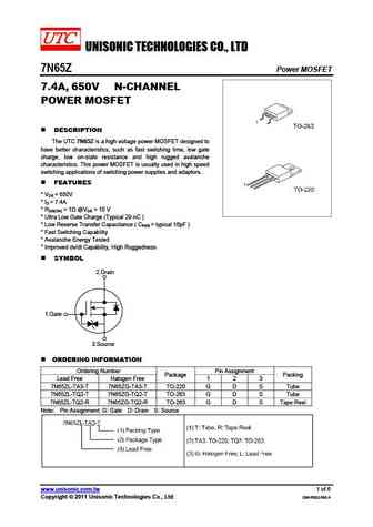
UNISONIC TECHNOLOGIES CO., LTD 7N65Z Power MOSFET 7.4A, 650V N-CHANNEL POWER MOSFET DESCRIPTION The UTC 7N65Z is a high voltage power MOSFET designed to have better characteristics, such as fast switching time, low gate charge, low on-state resistance and high rugged avalanche characteristics. This power MOSFET is usually used in high speed switching applications of switchin
7n65l-tn3-r 7n65g-tn3-r 7n65l-t2q-t 7n65g-t2q-t 7n65l-tq2-t 7n65g-tq2-t 7n65l-tq2-r 7n65g-tq2-r 7n65g-tm3-t.pdf
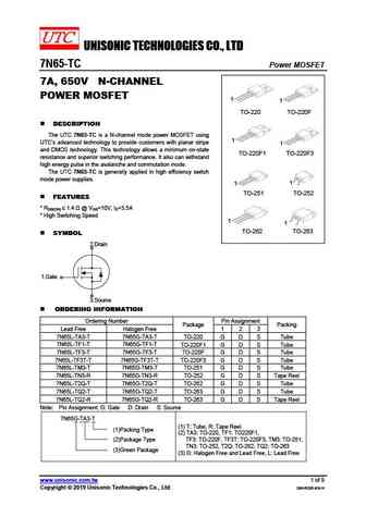
UNISONIC TECHNOLOGIES CO., LTD 7N65-TC Power MOSFET 7A, 650V N-CHANNEL POWER MOSFET 1 1 TO-220 TO-220F DESCRIPTION The UTC 7N65-TC is a N-channel mode power MOSFET using 1 UTC s advanced technology to provide customers with planar stripe 1 and DMOS technology. This technology allows a minimum on-state TO-220F3 TO-220F1 resistance and superior switching performance.
7n65kl-ta3-t 7n65kg-ta3-t 7n65kl-tf3-t 7n65kg-tf3-t 7n65kl-tf1-t 7n65kg-tf1-t 7n65kl-tf2-t.pdf
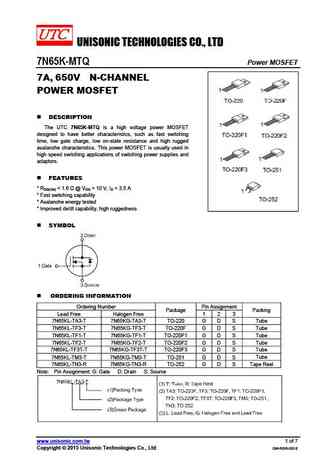
UNISONIC TECHNOLOGIES CO., LTD 7N65K-MTQ Power MOSFET 7A, 650V N-CHANNEL POWER MOSFET DESCRIPTION The UTC 7N65K-MTQ is a high voltage power MOSFET designed to have better characteristics, such as fast switching time, low gate charge, low on-state resistance and high rugged avalanche characteristics. This power MOSFET is usually used in high speed switching applications of s
7n65kl-ta3-t 7n65kg-ta3-t 7n65kl-tf3-t 7n65kg-tf3-t 7n65kl-tf1-t 7n65kg-tf1-t 7n65kl-tq2-t 7n65kg-tq2-t 7n65kl-tq2-r 7n65kg-tq2-r.pdf
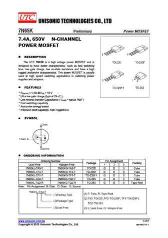
UNISONIC TECHNOLOGIES CO., LTD 7N65K Preliminary Power MOSFET 7.4A, 650V N-CHANNEL POWER MOSFET DESCRIPTION The UTC 7N65K is a high voltage power MOSFET and is designed to have better characteristics, such as fast switching time, low gate charge, low on-state resistance and have a high rugged avalanche characteristics. This power MOSFET is usually used at high speed switch
7n65kl-tf3t-t 7n65kg-tf3t-t 7n65kl-tm3-t 7n65kg-tm3-t 7n65kl-tn3-r 7n65kg-tn3-r 7n65kl-t2q-t 7n65kg-t2q-t.pdf
UNISONIC TECHNOLOGIES CO., LTD 7N65K-MTQ Power MOSFET 7.0A, 650V N-CHANNEL POWER MOSFET DESCRIPTION The UTC 7N65K-MTQ is a high voltage power MOSFET designed to have better characteristics, such as fast switching time, low gate charge, low on-state resistance and high rugged avalanche characteristics. This power MOSFET is usually used in high speed switching applications of
7n65l-ta3-t 7n65g-ta3-t 7n65l-tf1-t 7n65g-tf1-t 7n65l-tf2-t 7n65g-tf2-t 7n65l-tf3-t.pdf
UNISONIC TECHNOLOGIES CO., LTD 7N65-R Power MOSFET 7.4A, 650V N-CHANNEL POWER MOSFET DESCRIPTION The UTC 7N65-R is a high voltage power MOSFET and is designed to have better characteristics, such as fast switching time, low gate charge, low on-state resistance and have a high rugged avalanche characteristics. This power MOSFET is usually used at high speed switching applic
tsm7n65cz.pdf
TSM7N65 650V N-Channel Power MOSFET ITO-220 TO-220 Pin Definition PRODUCT SUMMARY 1. Gate 2. Drain VDS (V) RDS(on)( ) ID (A) 3. Source 650 1.2 @ VGS =10V 3 General Description The TSM7N65 N-Channel enhancement mode Power MOSFET is produced by planar stripe DMOS technology. This advanced technology has been especially tailored to minimize on-state resistance, provide supe
tsm7n65ci.pdf
TSM7N65 650V N-Channel Power MOSFET TO-220 ITO-220 Pin Definition PRODUCT SUMMARY 1. Gate VDS (V) RDS(on)( ) ID (A) 2. Drain 3. Source 650 1.2 @ VGS =10V 6.4 General Description The TSM7N65 N-Channel enhancement mode Power MOSFET is produced by planar stripe DMOS technology. This advanced technology has been especially tailored to minimize on-state resistance, provide
cjp07n65.pdf
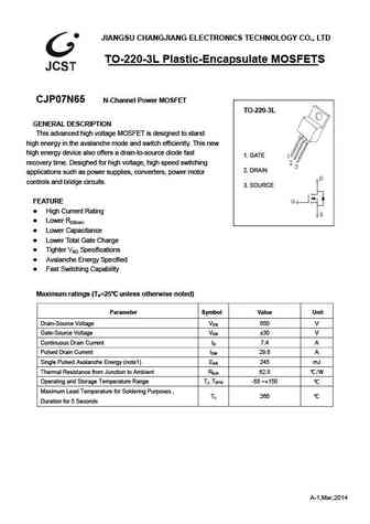
JIANGSU CHANGJIANG ELECTRONICS TECHNOLOGY CO., LTD TO-220-3L Plastic-Encapsulate MOSFETS CJP07N65 N-Channel Power MOSFET TO-220-3L GENERAL DESCRIPTION This advanced high voltage MOSFET is designed to stand high energy in the avalanche mode and switch efficiently. This new high energy device also offers a drain-to-source diode fast 1. GATE recovery time. Desighed for high vo
cjpf07n65.pdf
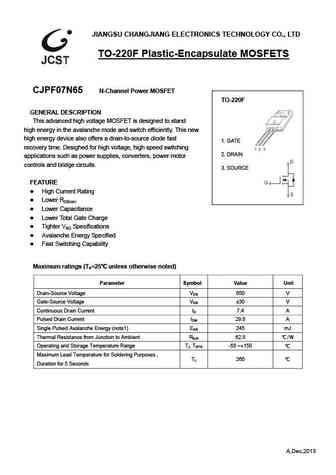
JIANGSU CHANGJIANG ELECTRONICS TECHNOLOGY CO., LTD TO-220F Plastic-Encapsulate MOSFETS CJPF07N65 N-Channel Power MOSFET TO-220F GENERAL DESCRIPTION This advanced high voltage MOSFET is designed to stand high energy in the avalanche mode and switch efficiently. This new high energy device also offers a drain-to-source diode fast 1. GATE recovery time. Desighed for high volta
kf7n65fm.pdf
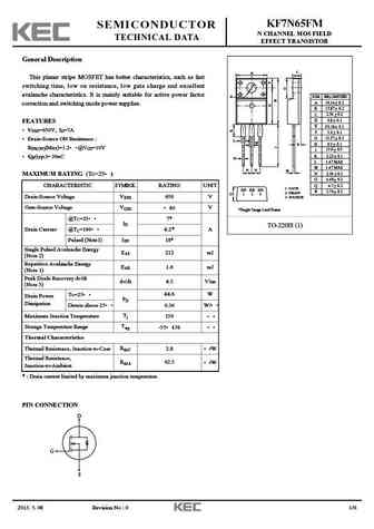
KF7N65FM SEMICONDUCTOR N CHANNEL MOS FIELD TECHNICAL DATA EFFECT TRANSISTOR General Description C A This planar stripe MOSFET has better characteristics, such as fast switching time, low on resistance, low gate charge and excellent avalanche characteristics. It is mainly suitable for active power factor E DIM MILLIMETERS _ A 10.16 0.2 + correction and switching mode power suppli
kf7n65p-f.pdf
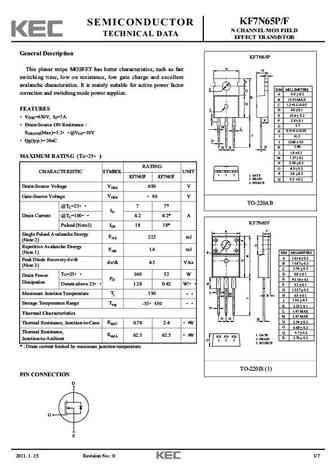
KF7N65P/F SEMICONDUCTOR N CHANNEL MOS FIELD TECHNICAL DATA EFFECT TRANSISTOR General Description KF7N65P A This planar stripe MOSFET has better characteristics, such as fast O C switching time, low on resistance, low gate charge and excellent F avalanche characteristics. It is mainly suitable for active power factor E DIM MILLIMETERS G correction and switching mode power suppli
apt47n65bc3g.pdf
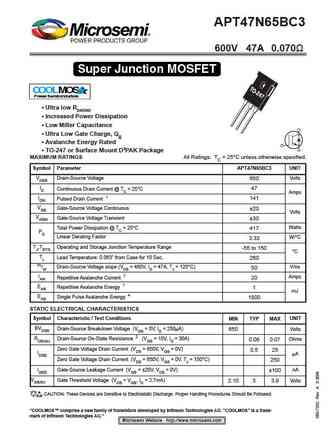
APT47N65BC3 600V 47A 0.070 Super Junction MOSFET COOLMOS Power Semiconductors D3 Ultra low RDS(ON) Increased Power Dissipation Low Miller Capacitance Ultra Low Gate Charge, Qg Avalanche Energy Rated TO-247 or Surface Mount D3PAK Package MAXIMUM RATINGS All Ratings TC = 25 C unless otherwise specified. Symbol Parameter APT47N65BC3 UNIT VDSS Drain-So
apt97n65b2c6 apt97n65lc6.pdf
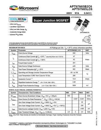
APT97N65B2C6 APT97N65LC6 650V 97A 0.041 APT97N65B2C6 COOLMOS Power Semiconductors Super Junction MOSFET T-Max TO-264 Ultra Low RDS(ON) Low Miller Capacitance Ultra Low Gate Charge, Qg Avalanche Energy Rated APT97N65LC6 Extreme dv/dt Rated D G Unless stated otherwise, Microsemi discrete MOSFETs contain a single MOSFET die. This device is made with
cep07n65 ceb07n65 cef07n65.pdf
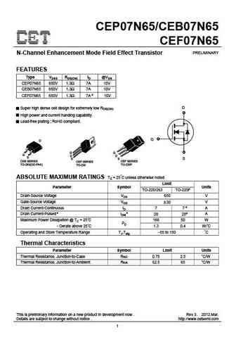
CEP07N65/CEB07N65 CEF07N65 PRELIMINARY N-Channel Enhancement Mode Field Effect Transistor FEATURES Type VDSS RDS(ON) ID @VGS CEP07N65 650V 1.3 7A 10V CEB07N65 650V 1.3 7A 10V CEF07N65 650V 1.3 7A d 10V D Super high dense cell design for extremely low RDS(ON). High power and current handing capability. Lead-free plating ; RoHS compliant. G S CEB SERIES CEP SERIES CEF SER
cep07n65a ceb07n65a cef07n65a.pdf
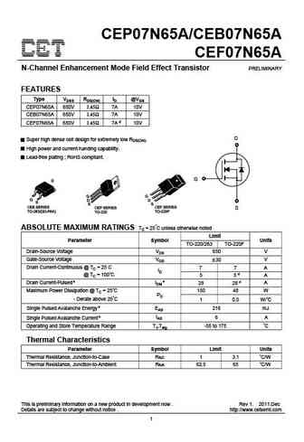
CEP07N65A/CEB07N65A CEF07N65A N-Channel Enhancement Mode Field Effect Transistor PRELIMINARY FEATURES Type VDSS RDS(ON) ID @VGS CEP07N65A 650V 1.45 7A 10V CEB07N65A 650V 1.45 7A 10V CEF07N65A 650V 1.45 7A d 10V D Super high dense cell design for extremely low RDS(ON). High power and current handing capability. Lead-free plating ; RoHS compliant. G CEB SERIES CEP SERIES CE
ced07n65a ceu07n65a.pdf
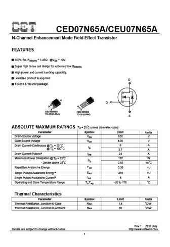
CED07N65A/CEU07N65A N-Channel Enhancement Mode Field Effect Transistor FEATURES 650V, 6A, RDS(ON) = 1.45 @VGS = 10V. Super high dense cell design for extremely low RDS(ON). High power and current handing capability. Lead free product is acquired. D TO-251 & TO-252 package. D G G S CEU SERIES CED SERIES TO-252(D-PAK) TO-251(I-PAK) S ABSOLUTE MAXIMUM RATINGS Tc = 25 C unless
ceu07n65a ced07n65a.pdf
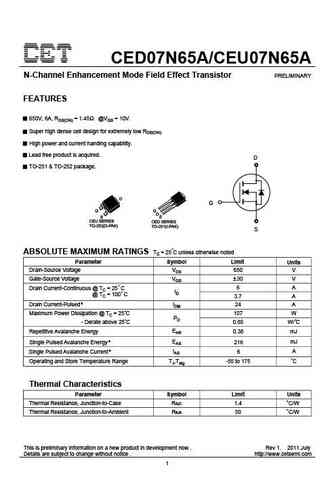
CED07N65A/CEU07N65A N-Channel Enhancement Mode Field Effect Transistor PRELIMINARY FEATURES 650V, 6A, RDS(ON) = 1.45 @VGS = 10V. Super high dense cell design for extremely low RDS(ON). High power and current handing capability. Lead free product is acquired. D TO-251 & TO-252 package. D G G S CEU SERIES CED SERIES TO-252(D-PAK) TO-251(I-PAK) S ABSOLUTE MAXIMUM RATINGS Tc =
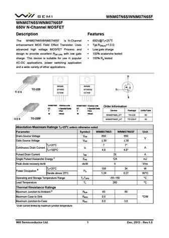
wnm07n65-f.pdf
WNM07N65/WNM07N65F WNM07N65/WNM07N65F 650V N-Channel MOSFET Description Features C The WNM07N65/WNM07N65F is N-Channel 650V@TJ=25 enhancement MOS Field Effect Transistor. Uses Typ.RDS(on)=1.0 advanced high voltage MOSFET Process and Low gate charge design to provide excellent RDS (ON) with low gate 100% avalanche tested charge. This device is suitable for use in p
h07n65.pdf
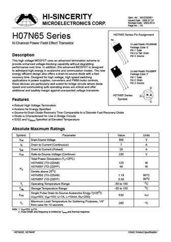
Spec. No. MOS200801 HI-SINCERITY Issued Date 2008.07.22 Revised Date 2009.0514 MICROELECTRONICS CORP. Page No. 1/6 H07N65 Series Pin Assignment H07N65 Series Tab N-Channel Power Field Effect Transistor 3-Lead Plastic TO-220AB Package Code E Pin 1 Gate Pin 2 & Tab Drain Description Pin 3 Source This high voltage MOSFET uses an advanced termination scheme
aot7n65.pdf

AOT7N65/AOTF7N65 650V, 7A N-Channel MOSFET General Description Product Summary VDS 750V@150 The AOT7N65 & AOTF7N65 have been fabricated using an advanced high voltage MOSFET process that is ID (at VGS=10V) 7A designed to deliver high levels of performance and RDS(ON) (at VGS=10V)
aod7n65 aoi7n65.pdf

AOD7N65/AOI7N65 650V,7A N-Channel MOSFET General Description Product Summary The AOD7N65 & AOI7N65 have been fabricated using an advanced high voltage MOSFET process that is designed VDS 750V@150 to deliver high levels of performance and robustness in ID (at VGS=10V) 7A popular AC-DC applications. RDS(ON) (at VGS=10V)
aot7n65 aotf7n65.pdf

AOT7N65/AOTF7N65 650V, 7A N-Channel MOSFET General Description Product Summary VDS 750V@150 The AOT7N65 & AOTF7N65 have been fabricated using an advanced high voltage MOSFET process that is ID (at VGS=10V) 7A designed to deliver high levels of performance and RDS(ON) (at VGS=10V)
aotf7n65.pdf
AOT7N65/AOTF7N65 650V, 7A N-Channel MOSFET General Description Product Summary VDS 750V@150 The AOT7N65 & AOTF7N65 have been fabricated using an advanced high voltage MOSFET process that is ID (at VGS=10V) 7A designed to deliver high levels of performance and RDS(ON) (at VGS=10V)
aoi7n65.pdf

AOD7N65/AOI7N65 650V,7A N-Channel MOSFET General Description Product Summary The AOD7N65 & AOI7N65 have been fabricated using an advanced high voltage MOSFET process that is designed VDS 750V@150 to deliver high levels of performance and robustness in ID (at VGS=10V) 7A popular AC-DC applications. RDS(ON) (at VGS=10V)
aod7n65.pdf
AOD7N65/AOI7N65 650V,7A N-Channel MOSFET General Description Product Summary The AOD7N65 & AOI7N65 have been fabricated using an advanced high voltage MOSFET process that is designed VDS 750V@150 to deliver high levels of performance and robustness in ID (at VGS=10V) 7A popular AC-DC applications. RDS(ON) (at VGS=10V)
afn07n65t220ft afn07n65t220t.pdf
AFN07N65 Alfa-MOS 650V / 7A N-Channel Technology Enhancement Mode MOSFET General Description Features AFN07N65 is an N-channel enhancement mode Power 650V/3.5A,RDS(ON)=1.4 (MAX)@VGS=10V MOSFET which is produced using VDMOS technology. The Low gate charge improved planar stripe cell and the improved guard ring Low Crss terminal have been especially tailored to minimize on-sta
sif7n65c.pdf
Shenzhen SI Semiconductors Co., LTD. Product Specification Shenzhen SI Semiconductors Co., LTD. Product Specification Shenzhen SI Semiconductors Co., LTD. Product Specification Shenzhen SI Semiconductors Co., LTD. Product Specification N- MOS / N-CHANNEL POWER MOSFET SIF7N65C N- MOS / N-CHANNEL POWER MOSFET SIF7N65C N
sif7n65d.pdf
Shenzhen SI Semiconductors Co., LTD. Product Specification Shenzhen SI Semiconductors Co., LTD. Product Specification Shenzhen SI Semiconductors Co., LTD. Product Specification Shenzhen SI Semiconductors Co., LTD. Product Specification N- MOS / N-CHANNEL POWER MOSFET SIF7N65D N- MOS / N-CHANNEL POWER MOSFET SIF7N65D N
jcs7n65bb jcs7n65sb jcs7n65cb jcs7n65fb.pdf
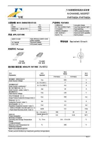
N R N-CHANNEL MOSFET JCS7N65B MAIN CHARACTERISTICS ID 7.0 A VDSS 650 V Package Rdson-max 1.3 (@Vgs=10V Qg-typ 25 nC APPLICATIONS High frequency switching mode power supply Electronic ballast LED LED power supply
jcs7n65ve jcs7n65re jcs7n65ce jcs7n65se jcs7n65be jcs7n65fe.pdf
N R N-CHANNEL MOSFET JCS7N65E MAIN CHARACTERISTICS Package ID 7.0 A VDSS 650 V Rdson-max 1.1 @Vgs=10V Qg-typ 23 nC APPLICATIONS High frequency switching mode power supply Electronic ballast LED LED power supply
mtn7n65fp.pdf
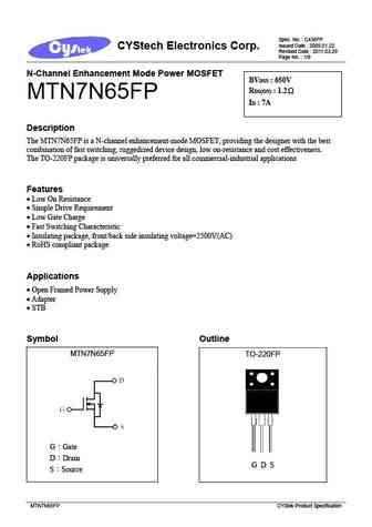
Spec. No. C436FP Issued Date 2009.01.22 CYStech Electronics Corp. Revised Date 2011.03.29 Page No. 1/9 N-Channel Enhancement Mode Power MOSFET BVDSS 650V RDS(ON) 1.2 MTN7N65FP ID 7A Description The MTN7N65FP is a N-channel enhancement-mode MOSFET, providing the designer with the best combination of fast switching, ruggedized device design, low on-resistanc
7n65a 7n65af.pdf
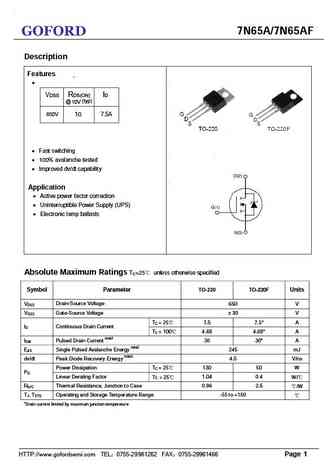
7N65A/7N65AF GOFORD Description Features - VDSS RDS(ON) ID @ 10V (typ) 7.5A 650V 1 Fast switching 100% avalanche tested Improved dv/dt capability Application Active power factor correction Uninterruptible Power Supply (UPS) Electronic lamp ballasts Absolute Maximum Ratings TC=25 unless otherwise specified Symbol Parameter TO-220
g7n65.pdf
GOFORD G7N65 Description Features VDSS RDS(ON) ID @ 10V (typ) 7.5 A 650V 1 Fast switching 100% avalanche tested Improved dv/dt capability Application Active power factor correction Uninterruptible Power Supply (UPS) Electronic lamp ballasts Absolute Maximum Ratings TC=25 unless otherwise specified Max. Symbol Parameter Units TO
sdu07n65 sdd07n65.pdf
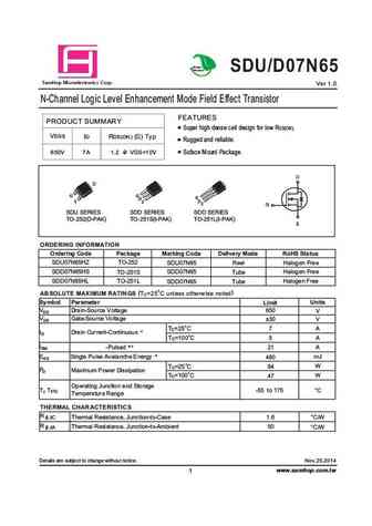
Green Product SDU/D07N65 a S mHop Microelectronics C orp. Ver 1.0 N-Channel Logic Level Enhancement Mode Field Effect Transistor FEATURES PRODUCT SUMMARY Super high dense cell design for low RDS(ON). VDSS ID RDS(ON) ( ) Typ Rugged and reliable. 650V 7A 1.2 @ VGS=10V Suface Mount Package. D G G S S SDU SERIES SDD SERIES SDD SERIES TO-252(D-PAK) TO-251S(I-PAK) TO-251L(I-PAK) O
sp07n65.pdf
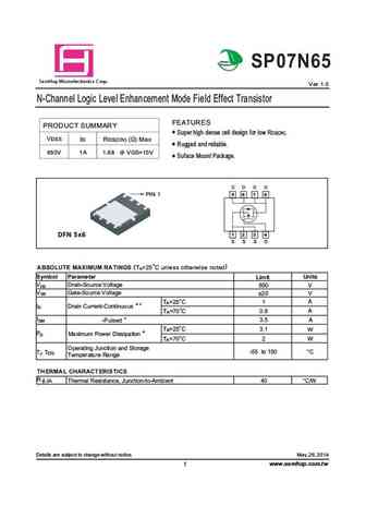
Green Product SP07N65 a S mHop Microelectronics C orp. Ver 1.0 N-Channel Logic Level Enhancement Mode Field Effect Transistor FEATURES PRODUCT SUMMARY Super high dense cell design for low RDS(ON). VDSS ID RDS(ON) ( ) Max Rugged and reliable. 650V 1A 1.68 @ VGS=10V Suface Mount Package. PIN 1 5 6 7 8 DFN 5x6 1 2 3 4 (TA=25 C unless otherwise noted) ABSOLUTE MAXIMUM RATINGS Sy
sdf07n65 sdp07n65.pdf
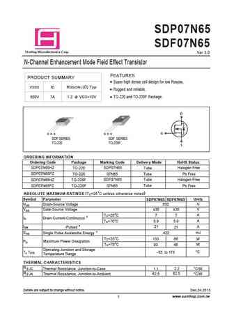
SDP07N65 SDF07N65 a S mHop Microelectronics C orp. Ver 3.0 N-Channel Enhancement Mode Field Effect Transistor FEATURES PRODUCT SUMMARY Super high dense cell design for low RDS(ON). VDSS ID RDS(ON) ( ) Typ Rugged and reliable. 650V 7A 1.2 @ VGS=10V TO-220 and TO-220F Package. D G G D S G D S SDP SERIES SDF SERIES TO-220 TO-220F S ORDERING INFORMATION Ordering Code Package Mar
ssf7n65f.pdf
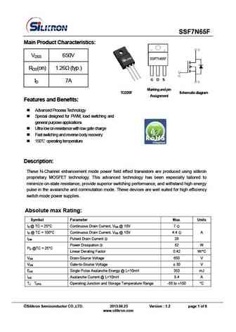
SSF7N65F Main Product Characteristics VDSS 650V RDS(on) 1.26 (typ.) ID 7A Marking and p in TO220F Schematic diagram Assignment Features and Benefits Advanced Process Technology Special designed for PWM, load switching and general purpose applications Ultra low on-resistance with low gate charge Fast switching and reverse body recovery 150
brf7n65.pdf
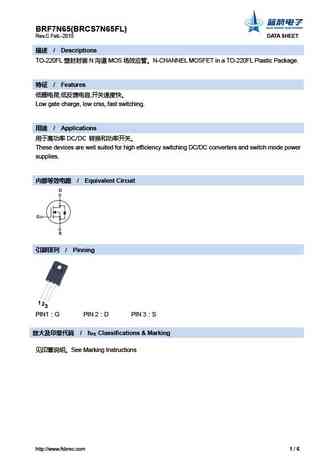
BRF7N65(BRCS7N65FL) Rev.C Feb.-2015 DATA SHEET / Descriptions TO-220FL N MOS N-CHANNEL MOSFET in a TO-220FL Plastic Package. / Features , , Low gate charge, low crss, fast switching. / Applications DC/DC These devices are well suited for
br7n65.pdf
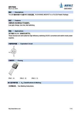
BR7N65 Rev. G Jul.-2018 DATA SHEET / Descriptions TO-220 N MOS N-CHANNEL MOSFET in a TO-220 Plastic Package. / Features , , Low gate charge, low crss, fast switching. / Applications DC/DC These devices are well suited for high efficiency sw
brd7n65.pdf
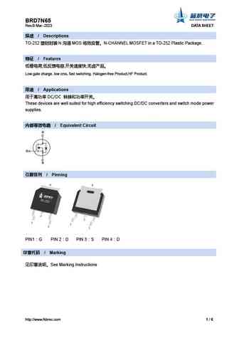
BRD7N65 Rev.B Mar.-2023 DATA SHEET / Descriptions TO-252 N MOS N-CHANNEL MOSFET in a TO-252 Plastic Package. / Features , , , Low gate charge, low crss, fast switching. Halogen-free Product,HF Product. / Applications DC/DC Thes
bri7n65.pdf
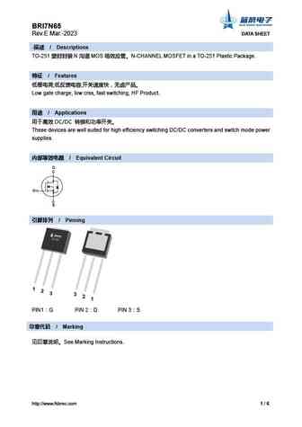
BRI7N65 Rev.E Mar.-2023 DATA SHEET - / Descriptions TO-251 N MOS N-CHANNEL MOSFET in a TO-251 Plastic Package. / Features , , Low gate charge, low crss, fast switching, HF Product. / Applications DC/DC These devices are well su
brb7n65.pdf
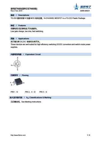
BRB7N65(BRCS7N65B) Rev.C Feb.-2015 DATA SHEET / Descriptions TO-263 N MOS N-CHANNEL MOSFET in a TO-252 Plastic Package. / Features , , Low gate charge, low crss, fast switching. / Applications DC/DC These devices are well suited for high
bra7n65.pdf
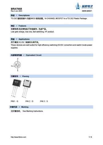
BRA7N65 Rev. A Jul.-2023 DATA SHEET / Descriptions TO-262 N MOS N-CHANNEL MOSFET in a TO-262 Plastic Package. / Features , , , Low gate charge, low crss, fast switching, HF product. / Applications DC/DC These devices are well sui
brd7n65s.pdf
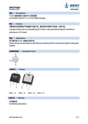
BRD7N65S Rev.A Dec.-2023 DATA SHEET / Descriptions TO-252 N MOS N-CHANNEL MOSFET in a TO-252 Plastic Package. / Features , , , Low gate charge, low crss, fast switching,HF Product. Have good Electromagnetic Interference porfo
brfl7n65.pdf
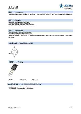
BRFL7N65 Rev.G Dec.-2017 DATA SHEET / Descriptions TO-220FL N MOS N-CHANNEL MOSFET in a TO-220FL Plastic Package. / Features , , Low gate charge, low crss, fast switching. / Applications DC/DC These devices are well suited for high effic
brfl7n65s.pdf
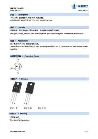
BRFL7N65S Rev.A Dec.-2023 DATA SHEET / Descriptions TO-220FL N MOS N-CHANNEL MOSFET in a TO-220FL Plastic Package. / Features Low gate charge, low crss, fast switching,Have good Electromagnetic Interference porformance. / Applications
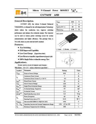
cs7n65 a4tdy.pdf
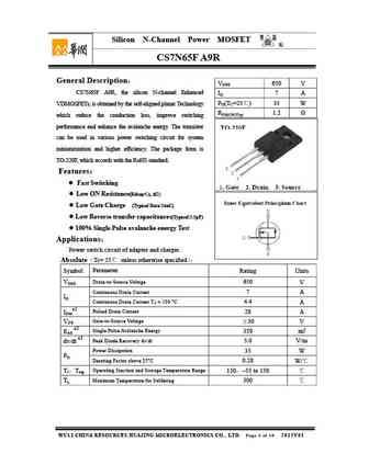
Silicon N-Channel Power MOSFET R CS7N65 A4TDY General Description VDSS 650 V CS7N65 A4TDY, the silicon N-channel Enhanced ID 7 A PD(TC=25 ) 95 W VDMOSFETs, is obtained by the self-aligned planar Technology RDS(ON)Typ 1.1 which reduce the conduction loss, improve switching performance and enhance the avalanche energy. The transistor can be used in various p
cs7n65 a4r.pdf
Silicon N-Channel Power MOSFET R CS7N65 A4R General Description VDSS 650 V CS7N65 A4R, the silicon N-channel Enhanced ID 7 A PD(TC=25 ) 100 W VDMOSFETs, is obtained by the self-aligned planar Technology RDS(ON)Typ 1.2 which reduce the conduction loss, improve switching performance and enhance the avalanche energy. The transistor can be used in various power
cs7n65f a9tdy.pdf
Silicon N-Channel Power MOSFET R CS7N65F A9TDY General Description VDSS 650 V CS7N65F A9TDY, the silicon N-channel Enhanced ID 7 A PD(TC=25 ) 40 W VDMOSFETs, is obtained by the self-aligned planar Technology RDS(ON)Typ 1.1 which reduce the conduction loss, improve switching performance and enhance the avalanche energy. The transistor can be used in various
cs7n65 a0d.pdf

Silicon N-Channel Power MOSFET R CS7N65 A0D General Description VDSS 650 V CS7N65 A0D, the silicon N-channel Enhanced ID 7 A PD(TC=25 ) 100 W VDMOSFETs, is obtained by the self-aligned planar Technology RDS(ON)Typ 0.98 which reduce the conduction loss, improve switching performance and enhance the avalanche energy. The transistor can be used in various powe
cs7n65 a3r.pdf

Silicon N-Channel Power MOSFET R CS7N65 A3R General Description VDSS 650 V CS7N65 A3R, the silicon N-channel Enhanced ID 7 A PD(TC=25 ) 100 W VDMOSFETs, is obtained by the self-aligned planar Technology RDS(ON)Typ 1.2 which reduce the conduction loss, improve switching performance and enhance the avalanche energy. The transistor can be used in various power
cs7n65 a3tdy.pdf
Silicon N-Channel Power MOSFET R CS7N65 A3TDY General Description VDSS 650 V CS7N65 A3TDY, the silicon N-channel Enhanced ID 7 A PD(TC=25 ) 95 W VDMOSFETs, is obtained by the self-aligned planar Technology RDS(ON)Typ 1.1 which reduce the conduction loss, improve switching performance and enhance the avalanche energy. The transistor can be used in various pow
cs7n65f a9r.pdf
Silicon N-Channel Power MOSFET R CS7N65F A9R General Description VDSS 650 V CS7N65F A9R, the silicon N-channel Enhanced ID 7 A PD(TC=25 ) 35 W VDMOSFETs, is obtained by the self-aligned planar Technology RDS(ON)Typ 1.2 which reduce the conduction loss, improve switching performance and enhance the avalanche energy. The transistor can be used in various power
cm7n65f.pdf
R C76F MN5 www.jdsemi.cn ShenZhen Jingdao Electronic Co.,Ltd. POWER MOSFET 650V N-Channel VDMOS RoHS 1 LD E 2 1 2
ftk7n65p f dd.pdf
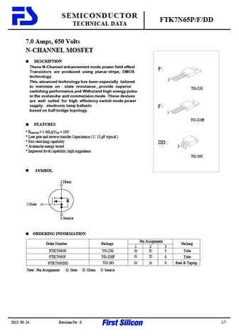
SEMICONDUCTOR FTK7N65P/F/DD TECHNICAL DATA 7.0 Amps, 650 Volts N-CHANNEL MOSFET DESCRIPTION These N-Channel enhancement mode power field effect P Transistors are produced using planar stripe, DMOS technology. 1 This advanced technology has been especially tailored to minimize on - state resistance , provide superior TO-220 switching performance,and Withstand high energy pulse
dhdsj7n65 dhbsj7n65.pdf
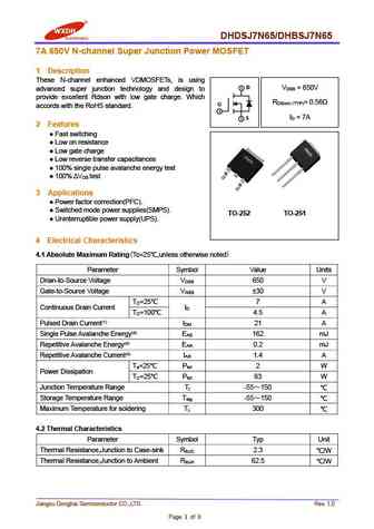
DHDSJ7N65/DHBSJ7N65 7A 650V N-channel Super Junction Power MOSFET 1 Description These N-channel enhanced VDMOSFETs, is using 2 D V = 650V DSS advanced super junction technology and design to provide excellent Rdson with low gate charge. Which R = 0.56 DS(on) (TYP) G accords with the RoHS standard. 1 I = 7A 3 S D 2 Features Fast switching Low on resistance
dhsj17n65 dhfsj17n65 dhisj17n65 dhesj17n65.pdf
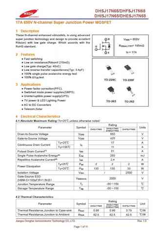
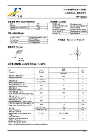
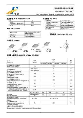
DHSJ17N65/DHFSJ17N65 DHISJ17N65/DHESJ17N65 17A 650V N-channel Super Junction Power MOSFET 1 Description These N-channel enhanced vdmosfets, is using advanced super junction technology and design to provide excellent 2 D V = 650V DSS Rds(on) with low gate charge. Which accords with the R = 185m DS(on) (TYP) RoHS standard. G 1 I = 17A 3 S D 2 Features Fast switching Low
dhd7n65.pdf
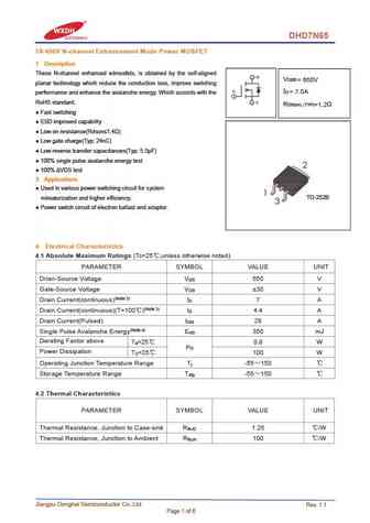
DHD7N65 7A 650V N-channel Enhancement Mode Power MOSFET 1 Description These N-channel enhanced vdmosfets, is obtained by the self-aligned V DSS = 650V planar technology which reduce the conduction loss, improve switching I = 7.0A D performance and enhance the avalanche energy. Which accords with the RoHS standard. R DS(on) TYP) =1.2 Fast switching ESD improved capabil
svs7n65dd2tr svs7n65fd2 svs7n65mjd2 svs7n65fjd2 svs7n65sd2 svs7n65sd2tr.pdf
SVS7N65D(F)(MJ)(FJ)(S)D2 7A, 650V MOS 2 SVS7N65D(F)(MJ)(FJ)(S)D2 N MOSFET 1 2 1 3 MOS TO-220F-3L 3 SVS7N65D(F)(MJ)(
svf7n65f-t.pdf
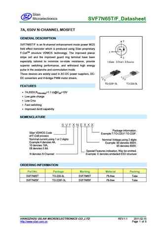
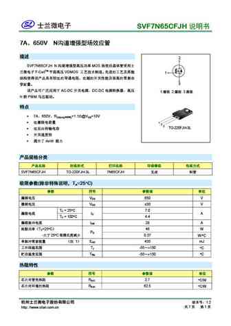
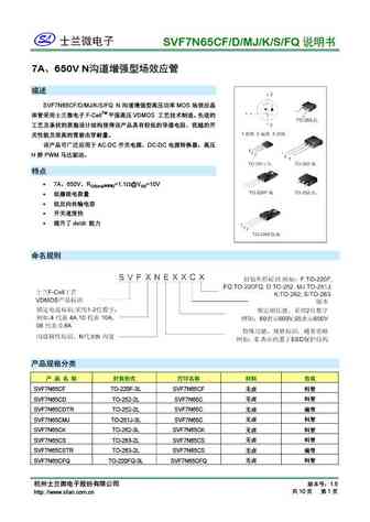
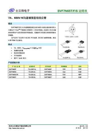
SVF7N65T/F_Datasheet 7A, 650V N-CHANNEL MOSFET GENERAL DESCRIPTION SVF7N65T/F is an N-channel enhancement mode power MOS field effect transistor which is produced using Silan proprietary F-CellTM structure VDMOS technology. The improved planar stripe cell and the improved guard ring terminal have been especially tailored to minimize on-state resistance, provide superior switching
svf7n65cf svf7n65cd svf7n65cmj svf7n65ck svf7n65ct.pdf
SVF7N65CF/D/MJ/K/T 7A 650V N 2 SVF7N65CF/D/MJ/K/T N MOS 1 F-CellTM VDMOS 1 2 3 TO-262-3L 3
svs7n65f svs7n65d svs7n65dtr svs7n65mj.pdf
SVS7N65F/D/MJ 7A, 650V MOS 2 SVS7N65F/D/MJ N MOSFET MOS 1 3 1 SVS7N65F / 3
mdf7n65bth.pdf
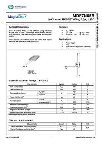
MDF7N65B N-Channel MOSFET 650V, 7.0A, 1.35 General Description Features These N-channel MOSFET are produced using advanced V = 650V DS MagnaChip s MOSFET Technology, which provides low on- I = 7.0A @ V = 10V D GS state resistance, high switching performance and excellent R 1.35 @ V = 10V DS(ON) GS quality. Applications These devices are suitable devic
msf7n65.pdf
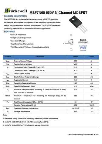
MSF7N65 650V N-Channel MOSFET GENERAL DESCRIPTION The MSF7N65 is a N-channel enhancement-mode MOSFET , providing the designer with the best combination of fast switching, ruggedized device design, low on-resistance and cost effectiveness. The TO-220F package is universally preferred for all commercial-industrial applications FEATURES Low On Resistance Simple Drive Requi
ru7n65l.pdf
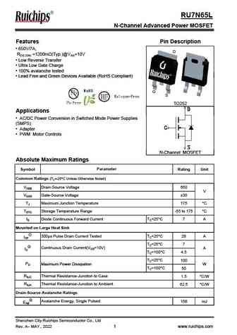
RU7N65L N-Channel Advanced Power MOSFET Features Pin Description 650V/7A, D RDS (ON) =1200m (Typ.)@VGS=10V Low Reverse Transfer Ultra Low Gate Charge 100% avalanche tested Lead Free and Green Devices Available (RoHS Compliant) Lead Free and Green Devices Available (RoHS Compliant) G S TO252 D D D D D D D Applications pp AC/DC Power Conversio
wfd7n65l.pdf
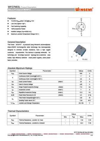
WFD7N65L Product Description Silicon N-Channel MOSFET Silicon N-Channel MOSFET Silicon N-Channel MOSFET Silicon N-Channel MOSFET Features D 7A,650V,R (Max1.38 )@V =10V DS(on) GS Low Crss (typical 15pF ) Fast Switching Capability G 100%Avalanche Tested Isolation Voltage (V =4000V AC) ISO Maximum Junction Temperature Range(150 ) S General Description
wff7n65s.pdf
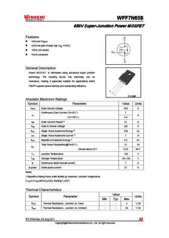
WFF7N65S WFF7N65S WFF7N65S WFF7N65S 650V Super-Junction Power MOSFET 650V Super-Junction Power MOSFET 650V Super-Junction Power MOSFET 650V Super-Junction Power MOSFET Features D Ultra low Rdson Ultra low gate charge (typ. Qg =19nC) 100% UIS tested G RoHS compliant S General Description Power MOSFET is fabricated using advanced super junction technology. The re
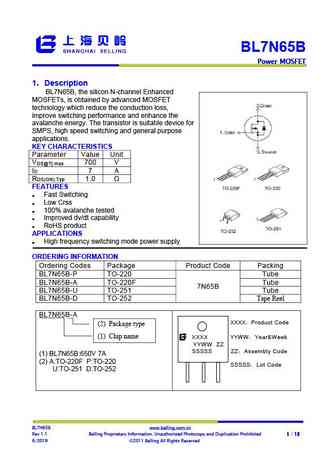
bl7n65b-p bl7n65b-a bl7n65b-u bl7n65b-d.pdf
BL7N65B Power MOSFET Power MOSFET Power MOSFET Power MOSFET 1 Description BL7N65B, the silicon N-channel Enhanced MOSFETs, is obtained by advanced MOSFET technology which reduce the conduction loss, improve switching performance and enhance the avalanche energy. The transistor is suitable device for SMPS, high speed switching and general purpose application
bl7n65a-p bl7n65a-a bl7n65a-u bl7n65a-d.pdf

BL7N65A Power MOSFET Power MOSFET Power MOSFET Power MOSFET 1 Description BL7N65A, the silicon N-channel Enhanced MOSFETs, is obtained by advanced MOSFET technology which reduce the conduction loss, improve switching performance and enhance the avalanche energy. The transistor is suitable device for SMPS, high speed switching and general purpose application
fhp7n65g.pdf
N N-CHANNEL MOSFET FHP7N65G MAIN CHARACTERISTICS FEATURES ID 7A Low gate charge VDSS 650V Crss ( 5.5pF) Low Crss (typical 5.5pF ) Rdson-typ @Vgs=10V 1.0 Fast switching Qg-typ 24nC 100% 100% avalanche tested dv/dt Improved dv/dt
fhp7n65a fhf7n65a.pdf
N N-CHANNEL MOSFET FHP7N65A /FHF7N65A MAIN CHARACTERISTICS FEATURES ID 7A Low gate charge VDSS 650V Crss ( 5.5pF) Low Crss (typical 5.5pF ) Rdson-typ @Vgs=10V 1.0 Fast switching Qg-typ 24nC 100% 100% avalanche tested dv/dt Impr
jfpc7n65c jffc7n65c.pdf
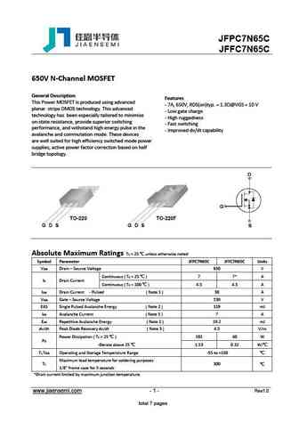
JFPC7N65C JFFC7N65C 650V N-Channel MOSFET General Description Features This Power MOSFET is produced using advanced - 7A, 650V, RDS(on)typ. = 1.3 @VGS = 10 V planar stripe DMOS technology. This advanced - Low gate charge technology has been especially tailored to minimize - High ruggedness on-state resistance, provide superior switching - Fast switching performance, a
jffc7n65e.pdf
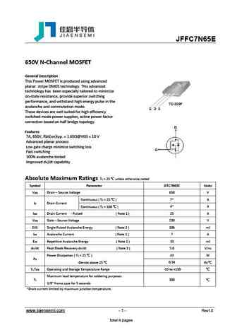
JFFC7N65E 650V N-Channel MOSFET General Description This Power MOSFET is produced using advanced planar stripe DMOS technology. This advanced technology has been especially tailored to minimize on-state resistance, provide superior switching performance, and withstand high energy pulse in the avalanche and commutation mode. These devices are well suited for high efficiency s
slp7n65c slf7n65c.pdf
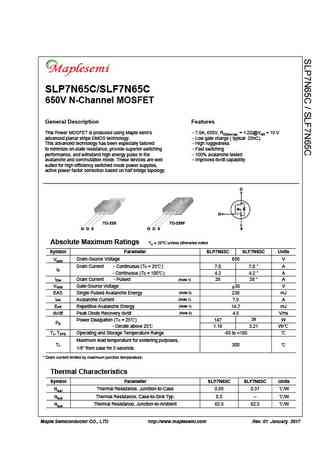
SLP7N65C/SLF7N65C 650V N-Channel MOSFET General Description Features This Power MOSFET is produced using Maple semi s - 7.0A, 650V, RDS(on) typ. = 1.2 @VGS = 10 V advanced planar stripe DMOS technology. - Low gate charge ( typical 25nC) This advanced technology has been especially tailored - High ruggedness to minimize on-state resistance, provide superior switching - Fast switching p
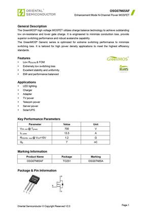
osg07n65af.pdf
OSG07N65AF Enhancement Mode N-Channel Power MOSFET General Description The GreenMOS high voltage MOSFET utilizes charge balance technology to achieve outstanding low on-resistance and lower gate charge. It is engineered to minimize conduction loss, provide superior switching performance and robust avalanche capability. The GreenMOS Generic series is optimized for extreme switchi
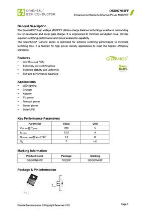
osg07n65ff.pdf
OSG07N65FF Enhancement Mode N-Channel Power MOSFET General Description The GreenMOS high voltage MOSFET utilizes charge balance technology to achieve outstanding low on-resistance and lower gate charge. It is engineered to minimize conduction loss, provide superior switching performance and robust avalanche capability. The GreenMOS Generic series is optimized for extreme switchi
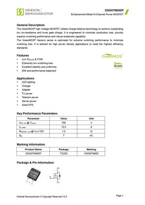
osg07n65df.pdf
OSG07N65DF Enhancement Mode N-Channel Power MOSFET General Description The GreenMOS high voltage MOSFET utilizes charge balance technology to achieve outstanding low on-resistance and lower gate charge. It is engineered to minimize conduction loss, provide superior switching performance and robust avalanche capability. The GreenMOS Generic series is optimized for extreme switchi
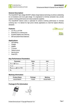
osg07n65pf.pdf
OSG07N65PF Enhancement Mode N-Channel Power MOSFET General Description The GreenMOS high voltage MOSFET utilizes charge balance technology to achieve outstanding low on-resistance and lower gate charge. It is engineered to minimize conduction loss, provide superior switching performance and robust avalanche capability. The GreenMOS Generic series is optimized for extreme switchi
pta07n65b.pdf
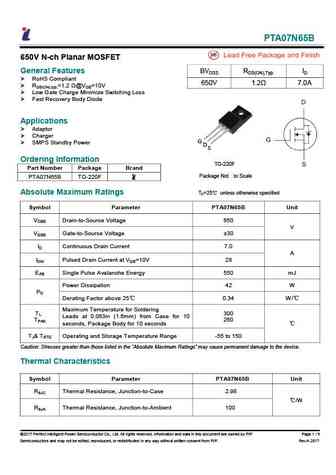
PTA07N65B 650V N-ch Planar MOSFET General Features BVDSS RDS(ON),Typ. ID RoHS Compliant 650V 1.2 7.0A RDS(ON),typ.=1.2 @VGS=10V Low Gate Charge Minimize Switching Loss Fast Recovery Body Diode Applications Adaptor Charger G SMPS Standby Power D S Ordering Information TO-220F Part Number Package Brand Package Not to Scale P
psu07n65 psd07n65.pdf
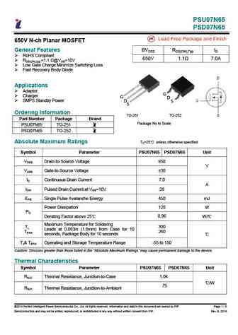
PSU07N65 PSD07N65 650V N-ch Planar MOSFET General Features BVDSS RDS(ON),Typ. ID RoHS Compliant 650V 1.1 7.0A RDS(ON),typ.=1.1 @VGS=10V Low Gate Charge Minimize Switching Loss Fast Recovery Body Diode Applications Adaptor G Charger G D SMPS Standby Power D S S Ordering Information TO-251 TO-252 Part Number Package Brand
psa07n65.pdf
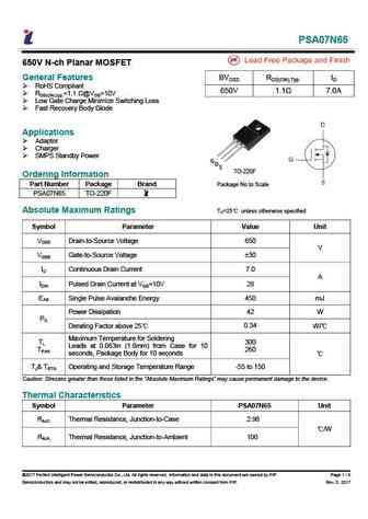
PSA07N65 650V N-ch Planar MOSFET General Features BVDSS RDS(ON),Typ. ID RoHS Compliant 650V 1.1 7.0A RDS(ON),typ.=1.1 @VGS=10V Low Gate Charge Minimize Switching Loss Fast Recovery Body Diode Applications Adaptor Charger SMPS Standby Power G D S TO-220F Ordering Information Part Number Package Brand Package No to Scale PSA07N6
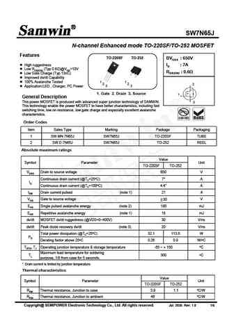
swb7n65dw.pdf
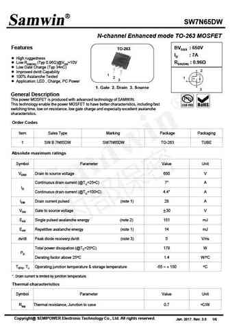
SW7N65DW N-channel Enhanced mode TO-263 MOSFET Features BVDSS 650V TO-263 ID 7A High ruggedness Low RDS(ON) (Typ 0.96 )@VGS=10V RDS(ON) 0.96 Low Gate Charge (Typ 34nC) 2 Improved dv/dt Capability 1 100% Avalanche Tested 2 1 3 Application LED , Charge, PC Power 1. Gate 2. Drain 3. Source 3 General Description This power
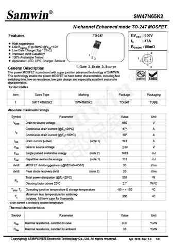
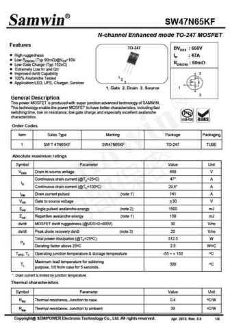
sw47n65k2 swt47n65k2.pdf
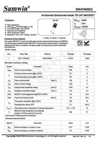
SW47N65K2 N-channel Enhanced mode TO-247 MOSFET TO-247 BVDSS 650V Features ID 47A High ruggedness RDS(ON) 56m Low RDS(ON) (Typ 56m )@VGS=10V Low Gate Charge (Typ 103nC) 2 Improved dv/dt Capability 1 100% Avalanche Tested 2 1 3 Application LED, UPS, Charge, Servicer 1. Gate 2. Drain 3. Source 3 General Description This p
swt47n65k2.pdf
SW47N65K2 N-channel Enhanced mode TO-247 MOSFET TO-247 BVDSS 650V Features ID 47A High ruggedness RDS(ON) 56m Low RDS(ON) (Typ 56m )@VGS=10V Low Gate Charge (Typ 103nC) 2 Improved dv/dt Capability 1 100% Avalanche Tested 2 1 3 Application LED, UPS, Charger, Servicer 1. Gate 2. Drain 3. Source 3 General Description This
swt47n65k2f.pdf
SW47N65K2F N-channel Enhanced mode TO-247 MOSFET Features TO-247 BVDSS 650V ID 47A High ruggedness Low RDS(ON) (Typ 59m )@VGS=10V RDS(ON) 59m Low Gate Charge (Typ 102nC) Improved dv/dt Capability 2 1 100% Avalanche Tested 2 1 3 Application Charger, UPS , LED , Servicer 1. Gate 2. Drain 3. Source 3 General Description Th
swt47n65k.pdf
SW47N65K N-channel Enhanced mode TO-247 MOSFET Features BVDSS 650V TO-247 ID 47A High ruggedness Low RDS(ON) (Typ 60m )@VGS=10V RDS(ON) 60m Low Gate Charge (Typ 152nC) Improved dv/dt Capability 2 1 100% Avalanche Tested 2 3 Application Charger,LED,PC Power 1 1. Gate 2. Drain 3. Source 3 General Description This power MO
swf7n65dd swn7n65dd swd7n65dd.pdf
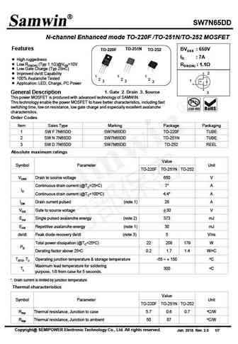
SW7N65DD N-channel Enhanced mode TO-220F /TO-251N/TO-252 MOSFET Features TO-251N TO-220F TO-252 BVDSS 650V ID 7A High ruggedness Low RDS(ON) (Typ 1.1 )@VGS=10V RDS(ON) 1.1 Low Gate Charge (Typ 28nC) 2 Improved dv/dt Capability 1 1 1 100% Avalanche Tested 2 2 2 1 3 3 3 Application LED, Charge, PC Power 1. Gate 2. Drain 3. So
swp7n65d swi7n65d swn7n65d swd7n65d swf7n65d swmn7n65d swj7n65d swha7n65d.pdf
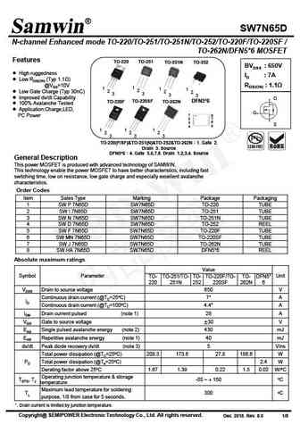
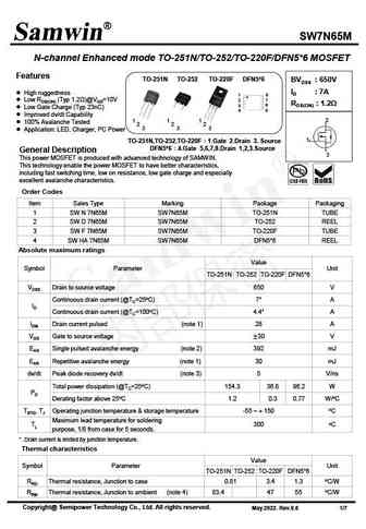
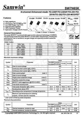
SW7N65D N-channel Enhanced mode TO-220/TO-251/TO-251N/TO-252/TO-220F/TO-220SF / TO-262N/DFN5*6 MOSFET Features TO-220 TO-251 TO-251N TO-252 BVDSS 650V High ruggedness ID 7A Low RDS(ON) (Typ 1.1 ) @VGS=10V RDS(ON) 1.1 1 1 1 1 2 2 Low Gate Charge (Typ 30nC) 2 2 3 3 3 3 Improved dv/dt Capability D DFN5*6 TO-220F TO-220SF TO-262N 100% Avalan
swf7n65k2 swi7n65k2 swn7n65k2 swd7n65k2.pdf
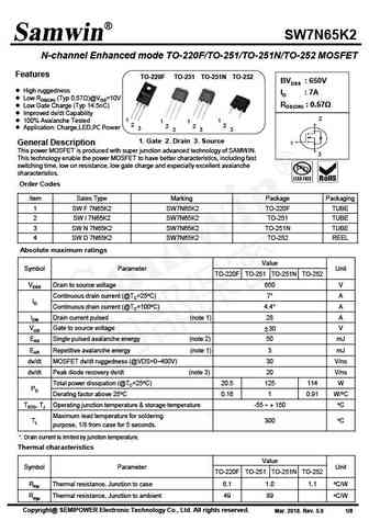
SW7N65K2 N-channel Enhanced mode TO-220F/TO-251/TO-251N/TO-252 MOSFET Features TO-220F TO-251 TO-251N TO-252 BVDSS 650V High ruggedness ID 7A Low RDS(ON) (Typ 0.57 )@VGS=10V RDS(ON) 0.57 Low Gate Charge (Typ 14.5nC) Improved dv/dt Capability 2 1 100% Avalanche Tested 1 1 1 2 2 2 2 Application Charge,LED,PC Power 3 3 3
swn7n65da swj7n65da swd7n65da.pdf
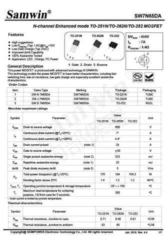
SW7N65DA N-channel Enhanced mode TO-251N/TO-262N/TO-252 MOSFET Features TO-262N TO-251N TO-252 BVDSS 650V High ruggedness ID 7A Low RDS(ON) (Typ 1.4 )@VGS=10V RDS(ON) 1.4 Low Gate Charge (Typ 25nC) Improved dv/dt Capability 2 1 1 1 100% Avalanche Tested 2 2 2 3 3 3 1 Application LED , Charge, PC Power 1. Gate 2. Drai
swt47n65kf.pdf
SW47N65KF N-channel Enhanced mode TO-247 MOSFET Features TO-247 BVDSS 650V High ruggedness ID 47A Low RDS(ON) (Typ 60m )@VGS=10V RDS(ON) 60m Low Gate Charge (Typ 152nC) Extremely Low trr and Qrr 2 Improved dv/dt Capability 1 100% Avalanche Tested 2 3 Application LED, UPS, Charger, Servicer 1 1. Gate 2. Drain 3. Source
swyn7n65d.pdf
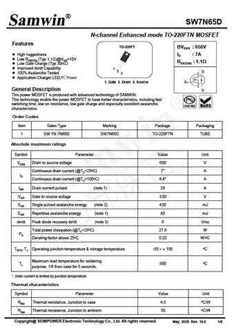
SW7N65D N-channel Enhanced mode TO-220FTN MOSFET Features TO-220FT BVDSS 650V High ruggedness ID 7A Low RDS(ON) (Typ 1.1 )@VGS=10V RDS(ON) 1.1 Low Gate Charge (Typ 30nC) Improved dv/dt Capability 1 2 D 100% Avalanche Tested 3 Application Charger,LED,PC Power 1. Gate 2. Drain 3. Source G General Description S This power MOSFET is produced wi
sw7n65d swp7n65d swi7n65d swn7n65d swd7n65d swf7n65d swmn7n65d swj7n65d swha7n65d.pdf

SW7N65D N-channel Enhanced mode TO-220/TO-251/TO-251N/TO-252/TO-220F/TO-220SF / TO-262N/DFN5*6 MOSFET Features TO-220 TO-251 TO-251N TO-252 BVDSS 650V High ruggedness ID 7A Low RDS(ON) (Typ 1.1 ) @VGS=10V RDS(ON) 1.1 1 1 1 1 2 2 Low Gate Charge (Typ 30nC) 2 2 3 3 3 3 Improved dv/dt Capability D DFN5*6 TO-220F TO-220SF TO-262N 100% Avalan
swn7n65m swd7n65m swf7n65m swha7n65m.pdf
SW7N65M N-channel Enhanced mode TO-251N/TO-252/TO-220F/DFN5*6 MOSFET Features TO-251N TO-252 TO-220F DFN5*6 BVDSS 650V ID 7A High ruggedness 1 8 Low RDS(ON) (Typ 1.2 )@VGS=10V 2 7 RDS(ON) 1.2 6 3 Low Gate Charge (Typ 23nC) 4 5 Improved dv/dt Capability 2 1 1 1 100% Avalanche Tested 2 2 2 3 3 3 Application LED, Charger, PC Power 1 TO-251
swf7n65k swmn7n65k swi7n65k swn7n65k swd7n65k swp7n65k.pdf
SW7N65K N-channel Enhanced mode TO-220F/TO-220SF/TO-251/TO- 251N/TO-252/TO-220 MOSFET Features TO-220F TO-220SF TO-251 TO-251N TO-252 TO-220 BVDSS 650V ID 7A High ruggedness Low RDS(ON) (Typ 0.5 )@VGS=10V RDS(ON) 0.5 Low Gate Charge (Typ 21nC) Improved dv/dt Capability 2 100% Avalanche Tested 1 1 1 1 1 1 2 2 2 2 2 2 Applica
swmn7n65j swd7n65j.pdf
SW7N65J N-channel Enhanced mode TO-220SF/TO-252 MOSFET Features TO-220SF TO-252 BVDSS 650V High ruggedness ID 7A Low RDS(ON) (Typ 0.6 )@VGS=10V RDS(ON) 0.6 Low Gate Charge (Typ 13nC) Improved dv/dt Capability 100% Avalanche Tested 1 1 2 2 2 Application LED , Charger, PC Power 3 3 1. Gate 2. Drain 3. Source 1 General Description This power MO
swp7n65d swi7n65d swn7n65d swui7n65d swd7n65d swf7n65d swmn7n65d swj7n65d swha7n65d swy7n65d.pdf
SW7N65D N-channel Enhanced mode TO-220/TO-251/TO-251N/TO-251U/TO-252/TO- 220F/TO-220SF/TO-262N/DFN5*6/TO-220FT MOSFET Features TO-220 TO-251 TO-251N TO-251U TO-252 BVDSS 650V High ruggedness ID 7A Low RDS(ON) (Typ 1.1 ) @VGS=10V RDS(ON) 1.1 1 1 1 1 1 2 2 Low Gate Charge (Typ 30nC) 2 2 2 3 3 3 3 3 Improved dv/dt Capability D TO-220FT TO-262N DFN
src7n65.pdf
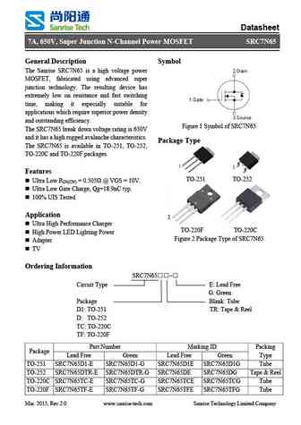
Datasheet 7A, 650V, Super Junction N-Channel Power MOSFET SRC7N65 General Description Symbol The Sanrise SRC7N65 is a high voltage power MOSFET, fabricated using advanced super junction technology. The resulting device has extremely low on resistance and fast switching time, making it especially suitable for applications which require superior power density and outstanding effic
srm7n65e1.pdf
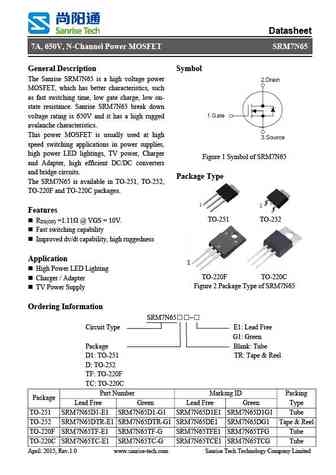
Datasheet 7A, 650V, N-Channel Power MOSFET SRM7N65 General Description Symbol The Sanrise SRM7N65 is a high voltage power MOSFET, which has better characteristics, such as fast switching time, low gate charge, low on- state resistance. Sanrise SRM7N65 break down voltage rating is 650V and it has a high rugged avalanche characteristics. This power MOSFET is usually used at high
srm7n65.pdf
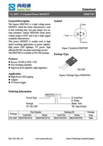
Datasheet 7A, 650V, N-Channel Power MOSFET SRM7N65 General Description Symbol The Sanrise SRM7N65 is a high voltage power MOSFET, which has better characteristics, such as fast switching time, low gate charge, low on- state resistance. Sanrise SRM7N65 break down voltage rating is 650V and it has a high rugged avalanche characteristics. This power MOSFET is usually used at high
sl7n65f sl7n65c.pdf

SL7N65 N-CHANNEL MOSFET MAIN CHARACTERISTICS 7A I D 650V V DSS 1.4 R V =10V DS(ON) GS 30nC Q G APPLICATIONS High efficiency switch mode power supplies Electronic lamp ballasts based on half bridge LED LED power supplies FEATURES 1 Gate Low
sl7n65.pdf
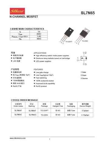
SL7N65 N-CHANNEL MOSFET MAIN CHARACTERISTICS 7A I D 650V V DSS 1.4 R V =10V DS(ON) GS 30nC Q G APPLICATIONS High efficiency switch mode power supplies Electronic lamp ballasts based on half bridge LED LED power supplies FEATURES 1 Gate Low
tmd7n65az tmu7n65az.pdf
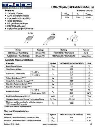
TMD7N65AZ(G)/TMU7N65AZ(G) Features N-channel MOSFET Low gate charge BVDSS ID RDS(on) 100% avalanche tested 650V 6.5A
tmp7n65az tmpf7n65az.pdf
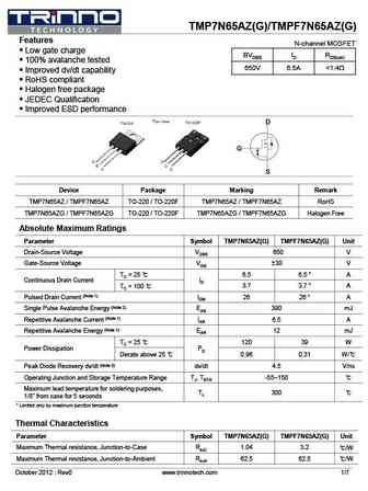
TMP7N65AZ(G)/TMPF7N65AZ(G) Features N-channel MOSFET Low gate charge BVDSS ID RDS(on) 100% avalanche tested 650V 6.5A
tmd7n65z tmu7n65z.pdf
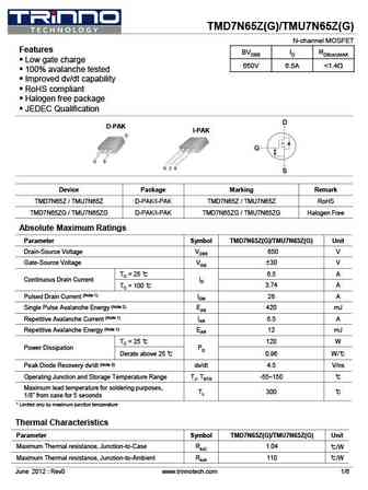
TMD7N65Z(G)/TMU7N65Z(G) N-channel MOSFET Features BVDSS ID RDS(on)MAX Low gate charge 650V 6.5A
tmp7n65z tmpf7n65z.pdf
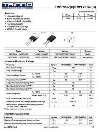
TMP7N65Z(G)/TMPF7N65Z(G) N-channel MOSFET Features BVDSS ID RDS(on) Low gate charge 650V 6.5A
tsp7n65m tsf7n65m.pdf
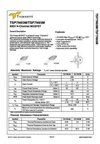
TSP7N65M/TSF7N65M 650V N-Channel MOSFET General Description Features This Power MOSFET is produced using Truesemi s 7A,650V,Max.RDS(on)=1.6 @ VGS =10V advanced planar stripe DMOS technology. This advanced technology has been especially tailored to Low gate charge(typical 29nC) minimize on-state resistance, provide superior switching High ruggedness performance, and wi
wmk7n65d1b wmh7n65d1b wml7n65d1b wmo7n65d1b.pdf
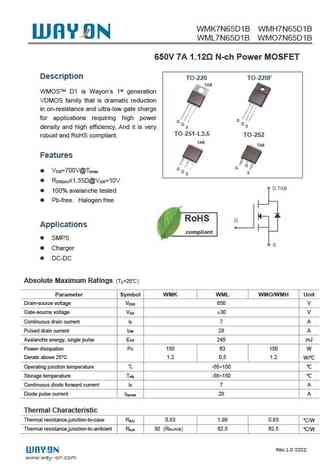
WMK7N65D1B WMH7N65D1B WML7N65D1B WMO7N65D1B 650V 7A 1.12 N-ch Power MOSFET Description TO-220 TO-220F TAB WMOSTM D1 is Wayon s 1st generation VDMOS family that is dramatic reduction in on-resistance and ultra-low gate charge for applications requiring high power G G D D S S density and high efficiency. And it is very TO-251-L3.5 TO-252 robust and RoHS compliant. TAB TAB
wml07n65c2 wmh07n65c2 wmm07n65c2 wmo07n65c2 wmp07n65c2 wmg07n65c2.pdf
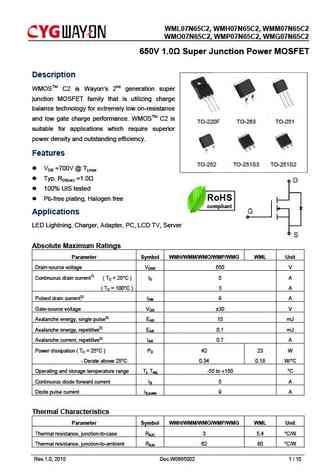
WML0 MM07N65C 07N65C2, WMH07N65C2, WM C2 WMO0 MG07N65C 07N65C2, WMP07N65C2, WM C2 650 Junction ET 0V 1.0 Super J n Power MOSFE Descrip ption WMOSTM C2 is Wa 2nd generation super ayon s n junction MOSFET fa that is utilizing charge M amily balance te or extremely esistance echnology fo y low on-re and low ga charge performanc WMOSTM C2 is ate ce. TO-220F TO TO-25
wmm07n65c4 wml07n65c4 wmo07n65c4 wmn07n65c4 wmp07n65c4 wmk07n65c4.pdf
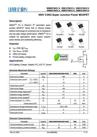
WMM0 65C4, MO07N65C 07N65C4, WML07N6 WM C4 WMN0 65C4, MK07N65C 07N65C4, WMP07N6 WM C4 650V 0.96 S T V Super Junction Power MOSFET Descrip ption WMOSTM C4 is Wa 4th generation super ayon s n junction MOSFET fa that is utilizing charge M amily S balance te or extremely esistance echnology fo y low on-re D S D G G G S D G and low ga charge performanc WM
cs7n65fa9tdy.pdf

Silicon N-Channel Power MOSFET R CS7N65F A9TDY General Description VDSS 650 V CS7N65F A9TDY, the silicon N-channel Enhanced ID 7 A PD(TC=25 ) 40 W VDMOSFETs, is obtained by the self-aligned planar Technology RDS(ON)Typ 1.1 which reduce the conduction loss, improve switching performance and enhance the avalanche energy. The transistor can be used in various
cs7n65a4tdy.pdf

Silicon N-Channel Power MOSFET R CS7N65 A4TDY General Description VDSS 650 V CS7N65 A4TDY, the silicon N-channel Enhanced ID 7 A PD(TC=25 ) 95 W VDMOSFETs, is obtained by the self-aligned planar Technology RDS(ON)Typ 1.1 which reduce the conduction loss, improve switching performance and enhance the avalanche energy. The transistor can be used in various p
cs7n65a0d.pdf
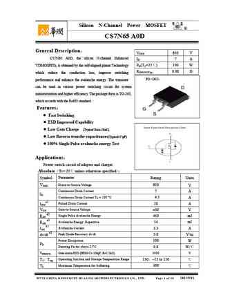
Silicon N-Channel Power MOSFET R CS7N65 A0D General Description VDSS 650 V CS7N65 A0D, the silicon N-channel Enhanced ID 7 A PD(TC=25 ) 100 W VDMOSFETs, is obtained by the self-aligned planar Technology RDS(ON)Typ 0.98 which reduce the conduction loss, improve switching performance and enhance the avalanche energy. The transistor can be used in various powe
cs7n65a3tdy.pdf

Silicon N-Channel Power MOSFET R CS7N65 A3TDY General Description VDSS 650 V CS7N65 A3TDY, the silicon N-channel Enhanced ID 7 A PD(TC=25 ) 95 W VDMOSFETs, is obtained by the self-aligned planar Technology RDS(ON)Typ 1.1 which reduce the conduction loss, improve switching performance and enhance the avalanche energy. The transistor can be used in various pow
cs7n65a3r.pdf
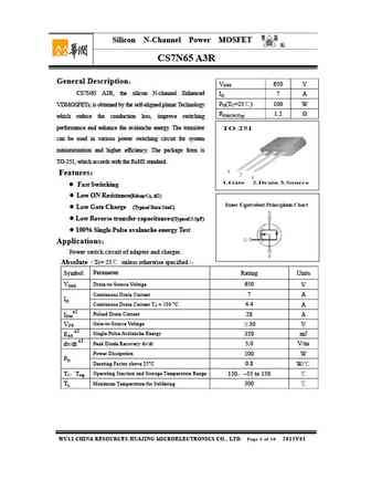
Silicon N-Channel Power MOSFET R CS7N65 A3R General Description VDSS 650 V CS7N65 A3R, the silicon N-channel Enhanced ID 7 A PD(TC=25 ) 100 W VDMOSFETs, is obtained by the self-aligned planar Technology RDS(ON)Typ 1.2 which reduce the conduction loss, improve switching performance and enhance the avalanche energy. The transistor can be used in various power
cs7n65a4r.pdf

Silicon N-Channel Power MOSFET R CS7N65 A4R General Description VDSS 650 V CS7N65 A4R, the silicon N-channel Enhanced ID 7 A PD(TC=25 ) 100 W VDMOSFETs, is obtained by the self-aligned planar Technology RDS(ON)Typ 1.2 which reduce the conduction loss, improve switching performance and enhance the avalanche energy. The transistor can be used in various power
cs7n65fa9r.pdf

Silicon N-Channel Power MOSFET R CS7N65F A9R General Description VDSS 650 V CS7N65F A9R, the silicon N-channel Enhanced ID 7 A PD(TC=25 ) 35 W VDMOSFETs, is obtained by the self-aligned planar Technology RDS(ON)Typ 1.2 which reduce the conduction loss, improve switching performance and enhance the avalanche energy. The transistor can be used in various power
cs7n65fa9d.pdf
Silicon N-Channel Power MOSFET R CS7N65F A9D General Description VDSS 650 V CS7N65F A9D, the silicon N-channel Enhanced ID 7 A PD(TC=25 ) 40 W VDMOSFETs, is obtained by the self-aligned planar Technology RDS(ON)Typ 0.98 which reduce the conduction loss, improve switching performance and enhance the avalanche energy. The transistor can be used in various po
atm7n65ate.pdf
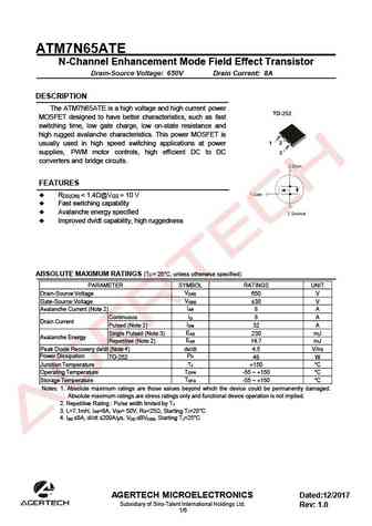
ATM7N65ATE N-Channel Enhancement Mode Field Effect Transistor Drain-Source Voltage 650V Drain Current 8A DESCRIPTION The ATM7N65ATE is a high voltage and high current power MOSFET designed to have better characteristics, such as fast switching time, low gate charge, low on-state resistance and high rugged avalanche characteristics. This power MOSFET is usually used in high spe
at7n65s.pdf
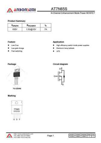
AT7N65S N-Channel Enhancement Mode Power MOSFET Product Summary V(BR)DSS RDS(on)MAX ID 650V 1.5 @10V 7A Feature Application Low Crss High efficiency switch mode power supplies Low gate charge Electronic lamp ballasts Fast switching UPS Package Circuit diagram TO-220AB Marking T7N65 XXXXX S G D Document ID Issued Date Revised Date Revision Page. Page 1 AS
cs7n65cf cs7n65cp cs7n65cu cs7n65cd.pdf
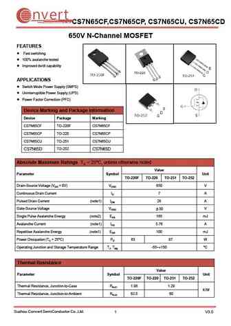
nvert Suzhou Convert Semiconductor Co ., Ltd. CS7N65CF,CS7N65CP, CS7N65CU, CS7N65CD 650V N-Channel MOSFET FEATURES Fast switching 100% avalanche tested Improved dv/dt capability APPLICATIONS Switch Mode Power Supply (SMPS) Uninterruptible Power Supply (UPS) Power Factor Correction (PFC) Device Marking and Package Information Device Package Marking CS7N65CF
cs7n65f cs7n65p cs7n65k.pdf
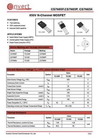
nvert Suzhou Convert Semiconductor Co ., Ltd. CS7N65F,CS7N65P, CS7N65K 650V N-Channel MOSFET FEATURES Fast switching 100% avalanche tested Improved dv/dt capability APPLICATIONS Switch Mode Power Supply (SMPS) Uninterruptible Power Supply (UPS) Power Factor Correction (PFC) Device Marking and Package Information Device Package Marking CS7N65F TO-220F CS7N65
fir7n65fg.pdf
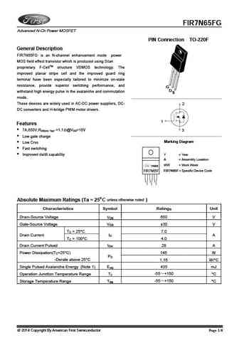
FIR7N65FG Advanced N-Ch Power MOSFET PIN Connection TO-220F General Description FIR7N65FG is an N-channel enhancement mode power MOS field effect transistor which is produced using Silan proprietary F-CellTM structure VDMOS technology. The improved planar stripe cell and the improved guard ring terminal have been especially tailored to minimize on-state resistance, provide superior
smf7n65.pdf
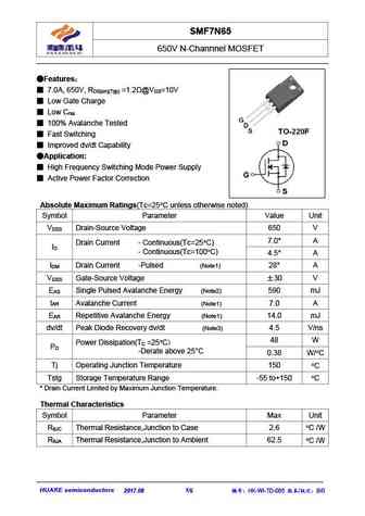
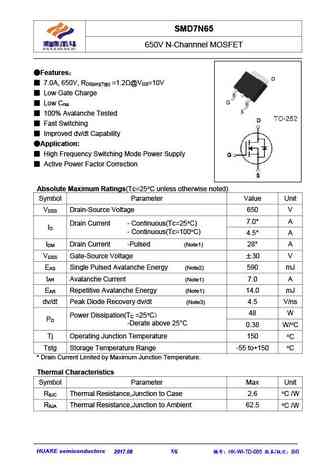
SMF7N65 650V N-Channnel MOSFET Features 7.0A, 650V, R =1.2 @V =10V DS(on)(Typ) GS Low Gate Charge Low C rss 100% Avalanche Tested Fast Switching Improved dv/dt Capability Application High Frequency Switching Mode Power Supply Active Power Factor Correction Absolute Maximum Ratings(Tc=25 C unless otherwise noted) Symbol Parameter Value
smd7n65.pdf
SMD7N65 650V N-Channnel MOSFET Features 7.0A, 650V, R =1.2 @V =10V DS(on)(Typ) GS Low Gate Charge Low C rss 100% Avalanche Tested Fast Switching Improved dv/dt Capability Application High Frequency Switching Mode Power Supply Active Power Factor Correction Absolute Maximum Ratings(Tc=25 C unless otherwise noted) Symbol Parameter Value
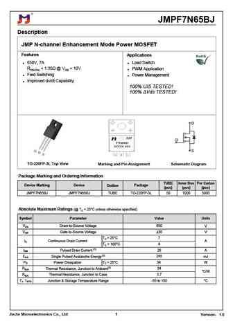
jmpf7n65bj.pdf
JMPF7N65BJ Description JMP N-channel Enhancement Mode Power MOSFET Features Applications 650V, 7A Load Switch RDS(ON)
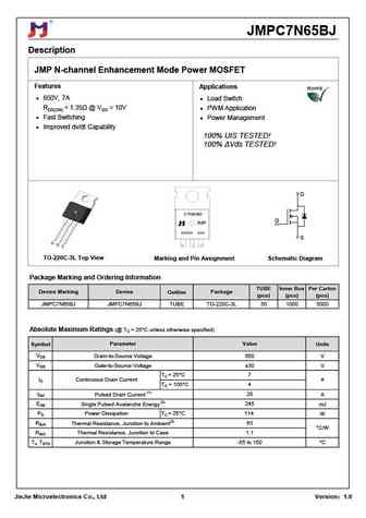
jmpc7n65bj.pdf
JMPC7N65BJ Description JMP N-channel Enhancement Mode Power MOSFET Features Applications 650V, 7A Load Switch RDS(ON)
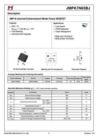
jmpk7n65bj.pdf
JMPK7N65BJ Description JMP N-channel Enhancement Mode Power MOSFET Features Applications 650V, 7A Load Switch RDS(ON)
lnc7n65d lnd7n65d lng7n65d lnh7n65d lnf7n65d.pdf
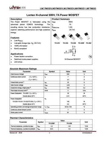
LNC7N65D LND7N65D LNG7N65D LNH7N65D LNF7N65D Lonten N-channel 650V, 7A Power MOSFET Description Product Summary The Power MOSFET is fabricated using the VDSS 650V advanced planar VDMOS technology. The ID 7A resulting device has low conduction resistance, RDS(on),max 1.4 superior switching performance and high avalance Qg,typ 20.7nC energy. Features Low RDS(on) Lo
si7n65.pdf
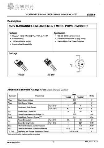
N-CHANNEL ENHANCEMENT MODE POWER MOSFET SI7N65 Description 650V N-CHANNEL ENHANCEMENT MODE POWER MOSFET Features Application R = 1.27 (Max.) @ V = 10V, I = 3.5A DC-DC & DC-AC Converters DS(ON) GS D Fast switching Uninterruptible Power Supply (UPS) 100% avalanche tested Switch Mode Low Power Supplies Improved dv/dt capability Package TO-220 TO-220
ptf7n65.pdf
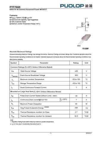
PTF7 N65 65 0V/7 A N-Channel A dv anced Power MOSFET Features RDS(on) (Typical 1.0 )@VGS=10V Improved dv/dt Capability, High Ruggedness 100% Avalanche Tested Maximum Junction Temperature Range (150 C) G D S TO-220F Absolute Maximum Ratings Stresses exceeding Maximum Ratings may damage the device. Maximum Ratings are stress ratings only. Functional operation above t
ptd7n65.pdf
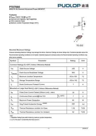
PTD7 N65 65 0V/7 A N-Channel A dv anced Power MOSFET Features RDS(on) (Typical 1.0 )@VGS=10V Improved dv/dt Capability, High Ruggedness 100% Avalanche Tested Maximum Junction Temperature Range (150 C) TO 252 Absolute Maximum Ratings Stresses exceeding Maximum Ratings may damage the device. Maximum Ratings are stress ratings only. Functional operation above the
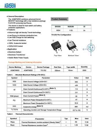
agm7n65d.pdf
AGM7N65D Table 3. Electrical Characteristics (TJ=25 unless otherwise noted) Symbol Parameter Conditions Min Typ Max Unit On/Off States BVDSS Drain-Source Breakdown Voltage V =0V I =250 A GS D 650 -- -- V Zero Gate Voltage Drain Current V =650V,V =0V -- -- 1 A DS GS I DSS Gate-Body Leakage Current V = 30V,V =0V -- -- nA GS DS I GSS 100 VGS(th) Gate Threshold Voltage
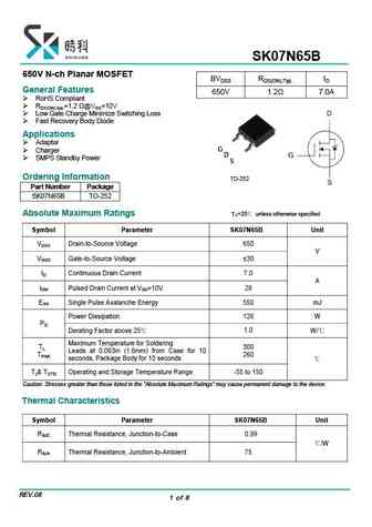
sk07n65b.pdf
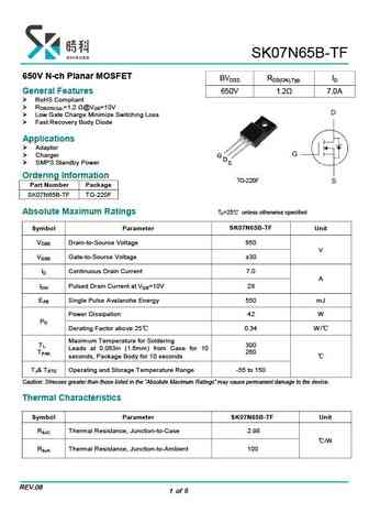
SK07N65B 650V N-ch Planar MOSFET BVDSS RDS(ON),Typ. ID General Features 650V 1.2 7.0A RoHS Compliant RDS(ON),typ.=1.2 @VGS=10V Low Gate Charge Minimize Switching Loss Fast Recovery Body Diode Applications Adaptor G Charger D SMPS Standby Power S Ordering Information TO-252 Part Number Package SK07N65B TO-252 Absolute Maximum Ratings =25 unle
spc7n65g.pdf
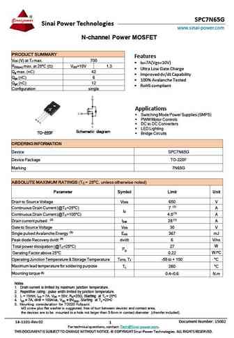
SPC7N65G Sinai Power Technologies www.sinai-power.com N-channel Power MOSFET PRODUCT SUMMARY Features V (V) at T max. 700 DS J ID=7A(Vgs=10V) R max. at 25oC ( ) V =10V 1.3 DS(on) GS Ultra Low Gate Charge Q max. (nC) 42 g Improved dv/dt Capability Q (nC) 6 gs 100% Avalanche Tested Q (nC) 12 gd RoHS compliant Configuration single Appl
spe7n65g.pdf
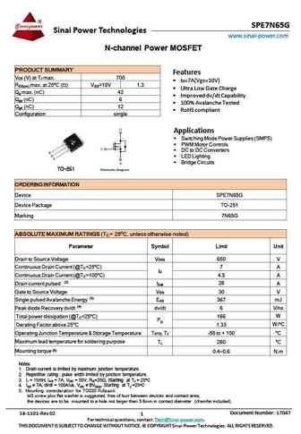
SPE7N65G Sinai Power Technologies www.sinai-power.com N-channel Power MOSFET PRODUCT SUMMARY Features V (V) at T max. 700 DS J ID=7A(Vgs=10V) R max. at 25oC ( ) V =10V 1.3 DS(on) GS Ultra Low Gate Charge Q max. (nC) 42 g Improved dv/dt Capability Q (nC) 6 gs 100% Avalanche Tested Q (nC) 12 gd RoHS compliant Configuration single Appli
spd7n65g.pdf
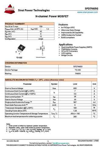
SPD7N65G Sinai Power Technologies www.sinai-power.com N-channel Power MOSFET PRODUCT SUMMARY Features V (V) at T max. 700 DS J ID=7A(Vgs=10V) R max. at 25oC ( ) V =10V 1.3 DS(on) GS Ultra Low Gate Charge Q max. (nC) 42 g Improved dv/dt Capability Q (nC) 6 gs 100% Avalanche Tested Q (nC) 12 gd RoHS compliant Configuration single Appli
ci47n65.pdf
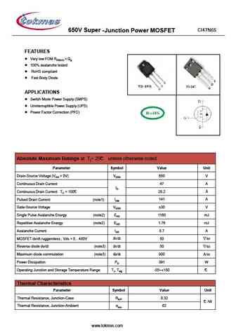
CI47N65 650V Super -Junction Power MOSFET FEATURES Very low FOM RDS(on) Qg 100% avalanche tested RoHS compliant Fast Body Diode APPLICATIONS Switch Mode Power Supply (SMPS) Uninterruptible Power Supply (UPS) Power Factor Correction (PFC) Absolute Maximum Ratings at Tj= 25 C unless otherwise noted Parameter Symbol Value Unit Drain-Source Voltage (VGS =
wsr7n65f.pdf
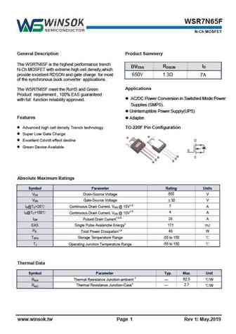
WSR7N65F N-Ch MOSFET General Description Product Summery The WSR7N65F is the highest performance trench RDSON ID BVDSS N-Ch MOSFET with extreme high cell density,which provide excellent RDSON and gate charge for most 650V 1.3 7A of the synchronous buck converter applications . Applications The WSR7N65F meet the RoHS and Green Product requirement , 100% EAS guaranteed
mt7n65.pdf
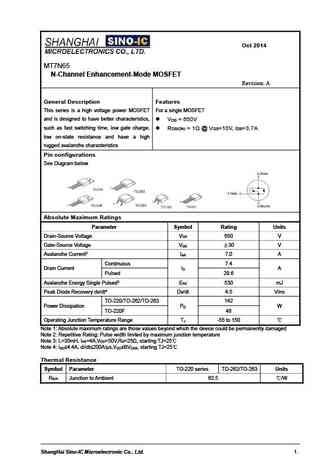
Oct 2014 MT7N65 N-Channel Enhancement-Mode MOSFET Revision A General Description Features This series is a high voltage power MOSFET For a single MOSFET and is designed to have better characteristics, V = 650V DS such as fast switching time, low gate charge, R = 1 @ V =10V, I =3.7A DS(ON) GS DS low on-state resistance and have a high rugged avalanche characteristics Pin
vs7n65af.pdf
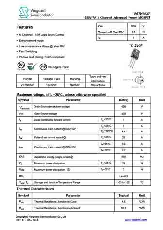
VS7N65AF 650V/7A N-Channel Advanced Power MOSFET V DS 650 V Features R DS(on),TYP@ VGS=10V 1.1 N-Channel 10V Logic Level Control I D 7 A Enhancement mode TO-220F Low on-resistance RDS(on) @ VGS=10V Fast Switching Pb-free lead plating; RoHS compliant Tape and reel Part ID Package Type Marking information VS7N65AF TO-220F 7N65AF 50pcs/Tube
vs7n65ad.pdf
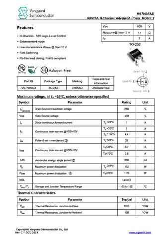
VS7N65AD 660V/7A N-Channel Advanced Power MOSFET V DS 660 V Features R DS(on),TYP@ VGS=10 V 1.1 N-Channel 10V Logic Level Control I D 7 A Enhancement mode TO-252 Low on-resistance RDS(on) @ VGS=10 V Fast Switching Pb-free lead plating; RoHS compliant Tape and reel Part ID Package Type Marking information VS7N65AD TO-252 7N65AD 2500pcs/
smirf7n65.pdf
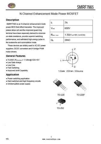
SMIRF7N65 30V /36A Single N Power MOSFET N-Channel Enhancement Mode Power MOSFET Description ID 7A SMIRF7N65 is an N-channel enhancement mode power MOS field effect transistor. The improved VDSS 650V planar stripe cell and the improved guard ring terminal have been especially tailored to minimize Rdson max 1.3 (VGS=10V, ID=3.5A) on-state resistance, provide superior s
vbzmb7n65.pdf
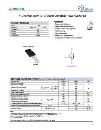
VBZMB7N65 www.VBsemi.com N-Channel (D-S) Super Junction Power MOSFET 900V FEATURES PRODUCT SUMMARY Dynamic dV/dt Rating VDS (V) 900 Available Repetitive Avalanche Rated RDS(on) ( )VGS = 10 V 0.95 RoHS* Isolated Central Mounting Hole Qg (Max.) (nC) 200 COMPLIANT Fast Switching Qgs (nC) 24 Qgd (nC) 110 Ease of Paralleling Configuration Single Simple
tma7n65h tmp7n65h tmd7n65h tmu7n65h.pdf
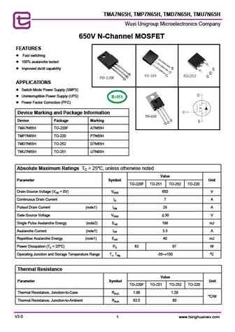
TMA7N65H, TMP7N65H, TMD7N65H, TMU7N65H Wuxi Unigroup Microelectronics Company 650V N-Channel MOSFET FEATURES l Fast switching l 100% avalanche tested l Improved dv/dt capability APPLICATIONS l Switch Mode Power Supply (SMPS) l Uninterruptible Power Supply (UPS) l Power Factor Correction (PFC) Device Marking and Package Information Device Package Marking TMA7N65H TO-220F A7N65H TM
hm7n65k hm7n65i.pdf
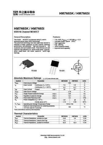
HM7N65K / HM7N65I HM7N65K / HM7N65I 650V N-Channel MOSFET General Description Features This Power MOSFET is produced using SL semi s 7.0A, 650V, RDS(on) = 1.35 @VGS = 10 V advanced planar stripe DMOS technology. Low gate charge ( typical 29nC) This advanced technology has been espe cially tailored to High ruggedness minimize o n-state r esistance, pr ovide superior sw
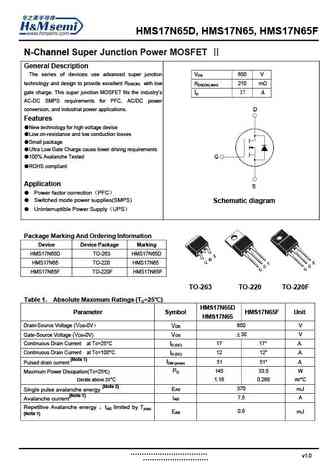
hms7n65i hms7n65k.pdf
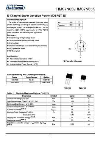
N-Channel Super Junction Power MOSFET General Description The series of devices use advanced trench gate super V 650 V DS junction technology and design to provide excellent RDS(ON) R 600 m DS(ON)TYP with low gate charge. This super junction MOSFET fits the ID 7 A industry s AC-DC SMPS requirements for PFC, AC/DC power conversion, and industrial powe
hms47n65a.pdf
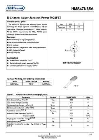
HMS47N65A N-Channel Super Junction Power MOSFET General Description The series of devices use advanced super junction VDS 650 V technology and design to provide excellent RDS(ON) with low RDS(ON) MAX 80 m gate charge. This super junction MOSFET fits the industry s ID A AC-DC SMPS requirements for PFC, AC/DC power conversion, and industrial power applications. Features
hm7n65 hm7n65f.pdf
/ / 650V N-Channel MOSFET General Description Features This Power MOSFET is produced using SL semi s 7.0A, 650V, RDS(on) = 1.26 @VGS = 10 V advanced planar stripe DMOS technology. Low gate charge ( typical 29nC) This advanced technology has been espe cially tailored to High ruggedness minimize o n-state r esistance, pr ovide superio
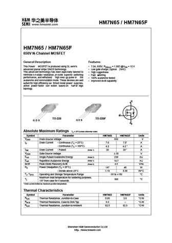
hms17n65 hms17n65f hms17n65d.pdf
HMS17N65D, HMS17N65, HMS17N65F N-Channel Super Junction Power MOSFET General Description The series of devices use advanced super junction VDS 650 V technology and design to provide excellent RDS(ON) with low RDS(ON) MAX 210 m gate charge. This super junction MOSFET fits the industry s ID 1 A AC-DC SMPS requirements for PFC, AC/DC power conversion, and industrial power app
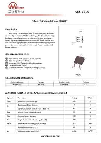
mdt7n65.pdf
Silicon N-Channel Power MOSFET Description MDT7N65, This Power MOSFET is produced using Wisdom s advanced planar stripe, DMOS technology. This latest technology has been especially designed to minimize on-state resistance, have a high rugged avalanche characteristics. These devices are well suited for high efficiency switch mode power supplies, active power factor correction, electroni
mpf7n65.pdf
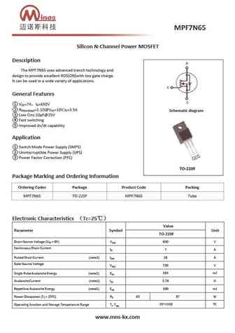
Silicon N-Channel Power MOSFET Description The MPF7N65 uses advanced trench technology and design to provide excellent RDS(ON)with low gate charge. It can be used in a wide variety of applications. General Features V =7A I =650V DS D R =1.1 @V =10V,I =3.5A DS(on)(typ) GS D Schematic diagram Low Crss 10pF@25V Fast switching Improved dv/dt capability Applicati
fxn7n65d.pdf
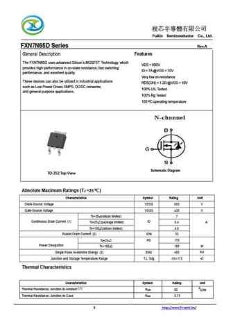
FuXin Semiconductor Co., Ltd. FXN7N65D Series Rev.A General Description Features The FXN7N65D uses advanced Silicon s MOSFET Technology, which VDS = 650V provides high performance in on-state resistance, fast switching ID = 7A @VGS = 10V performance, and excellent quality. Very low on-resistance These devices can also be utilized in industria
fxn7n65f.pdf
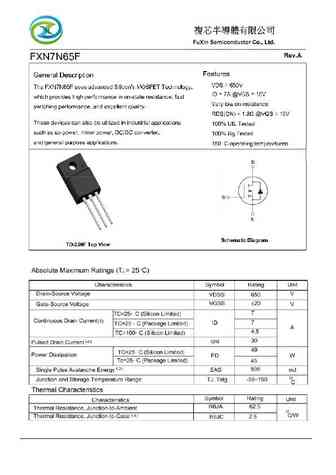
FXN7N65F Electrical Characteristics (TJ =25oC) Characteristics Symbol Test Condition Min Typ Max Unit Static Characteristics Drain-Source Breakdown Voltage BVDSS ID = 250 A, VGS = 0V 660 - - V Gate Threshold Voltage VGS(th) - 2.0 4.0 VDS = VGS, ID = 250 A Drain Cut-Off Current IDSS VDS = 650V, VGS = 0V 1.0 - - A VGS = 30V, VDS = 0V - 0.1 Gate Leakage Current
mpva7n65f.pdf
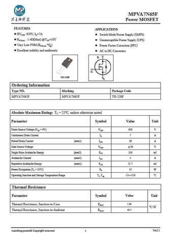
MPVA7N65F Power MOSFET MPSW60M041 FEATURES APPLICATIONS l BVDSS 650V, ID=7A l Switch Mode Power Supply (SMPS) l RDS(on) 1.4 (Max) @VGS=10V l Uninterruptible Power Supply (UPS) l Very Low FOM (RDS(on) *Qg) l Power Factor Correction (PFC) l Excellent stability and uniformity l AC to DC Converters D G TO-220F S Ordering Information Type NO. Marking Package Code MPVA7N65F M
hqb7n65c hqf7n65c.pdf
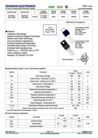
7N65 Series Product Parameter Specification 7A, 650V, N-Channel Power Field Effect Transistor Package Packing Quantity Quantity Quantity Industrial model Poplular name H Identificattion Method Per Tube Per Box Per Carton FQP7N65C HQB7N65C P TO-220P HAOHAI TUBE 50Pcs 1000Pcs 5000Pcs FQPF7N65C HQF7N65C F TO-220F 7N65 Series Pin Assignment ID=7A 3-Lead Plastic TO-220P Package Code P
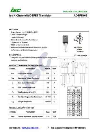
aot7n65.pdf
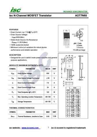
isc N-Channel MOSFET Transistor AOT7N65 FEATURES Drain Current I = 7.0A@ T =25 D C Drain Source Voltage- V =650V(Min) DSS Static Drain-Source On-Resistance R =1.56 (Max) DS(on) 100% avalanche tested Minimum Lot-to-Lot variations for robust device performance and reliable operation DESCRIPTION Designed for use in switch mode power supplies and general purpos
apt47n65bc3.pdf
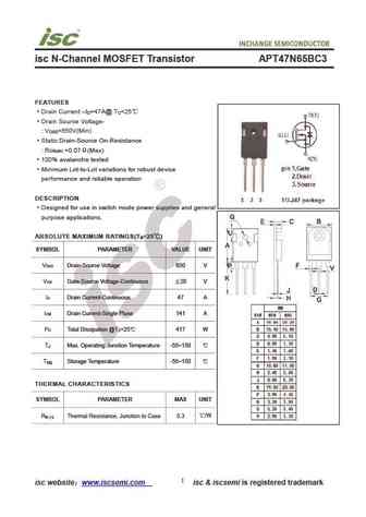
isc N-Channel MOSFET Transistor APT47N65BC3 FEATURES Drain Current I =47A@ T =25 D C Drain Source Voltage- V =650V(Min) DSS Static Drain-Source On-Resistance R =0.07 (Max) DS(on) 100% avalanche tested Minimum Lot-to-Lot variations for robust device performance and reliable operation DESCRIPTION Designed for use in switch mode power supplies and general purp
stb57n65m5.pdf
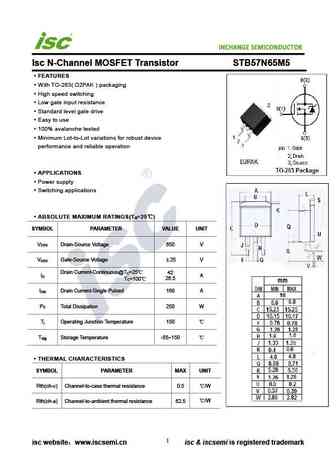
INCHANGE Semiconductor Isc N-Channel MOSFET Transistor STB57N65M5 FEATURES With TO-263( D2PAK ) packaging High speed switching Low gate input resistance Standard level gate drive Easy to use 100% avalanche tested Minimum Lot-to-Lot variations for robust device performance and reliable operation APPLICATIONS Power supply Switching applications ABSOLUTE MAXIM
dmg7n65sj3.pdf
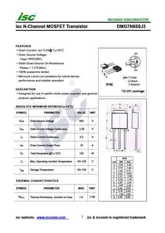
isc N-Channel MOSFET Transistor DMG7N65SJ3 FEATURES Drain Current I = 5.5A@ T =25 D C Drain Source Voltage- V = 650V(Min) DSS Static Drain-Source On-Resistance R = 1.4 (Max) DS(on) 100% avalanche tested Minimum Lot-to-Lot variations for robust device performance and reliable operation DESCRIPTION Designed for use in switch mode power supplies and general pu
dmg7n65scti.pdf
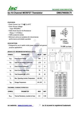
isc N-Channel MOSFET Transistor DMG7N65SCTI FEATURES Drain Current I = 7.7A@ T =25 D C Drain Source Voltage- V = 650V(Min) DSS Static Drain-Source On-Resistance R = 1.4 (Max) DS(on) 100% avalanche tested Minimum Lot-to-Lot variations for robust device performance and reliable operation DESCRIPTION Designed for use in switch mode power supplies and general p
fcpf067n65s3.pdf
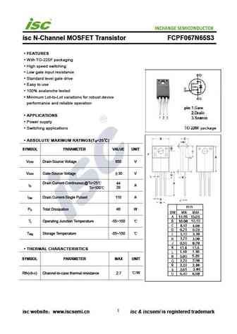
isc N-Channel MOSFET Transistor FCPF067N65S3 FEATURES With TO-220F packaging High speed switching Low gate input resistance Standard level gate drive Easy to use 100% avalanche tested Minimum Lot-to-Lot variations for robust device performance and reliable operation APPLICATIONS Power supply Switching applications ABSOLUTE MAXIMUM RATINGS(T =25 ) a SYMBO
spa07n65c3.pdf
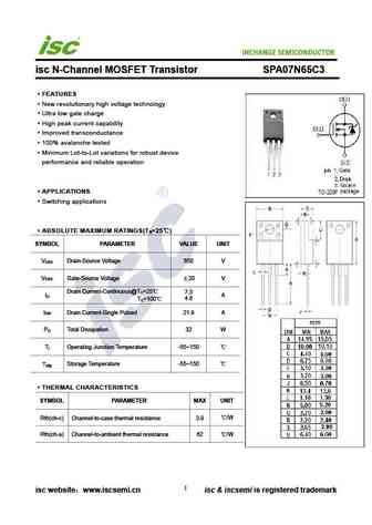
INCHANGE Semiconductor isc N-Channel MOSFET Transistor SPA07N65C3 FEATURES New revolutionary high voltage technology Ultra low gate charge High peak current capability Improved transconductance 100% avalanche tested Minimum Lot-to-Lot variations for robust device performance and reliable operation APPLICATIONS Switching applications ABSOLUTE MAXIMUM RATINGS(T =25
aotf7n65.pdf
isc N-Channel MOSFET Transistor AOTF7N65 FEATURES Drain Current I = 7.0A@ T =25 D C Drain Source Voltage- V =650V(Min) DSS Static Drain-Source On-Resistance R =1.56 (Max) DS(on) 100% avalanche tested Minimum Lot-to-Lot variations for robust device performance and reliable operation DESCRIPTION Designed for use in switch mode power supplies and general purpo
aoi7n65.pdf
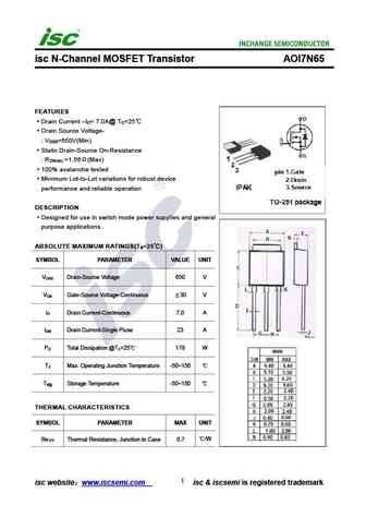
isc N-Channel MOSFET Transistor AOI7N65 FEATURES Drain Current I = 7.0A@ T =25 D C Drain Source Voltage- V =650V(Min) DSS Static Drain-Source On-Resistance R =1.56 (Max) DS(on) 100% avalanche tested Minimum Lot-to-Lot variations for robust device performance and reliable operation DESCRIPTION Designed for use in switch mode power supplies and general purpos
dmg7n65sct.pdf
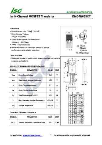
isc N-Channel MOSFET Transistor DMG7N65SCT FEATURES Drain Current I = 7.7A@ T =25 D C Drain Source Voltage- V = 650V(Min) DSS Static Drain-Source On-Resistance R = 1.4 (Max) DS(on) 100% avalanche tested Minimum Lot-to-Lot variations for robust device performance and reliable operation DESCRIPTION Designed for use in switch mode power supplies and general pu
fcp067n65s3.pdf
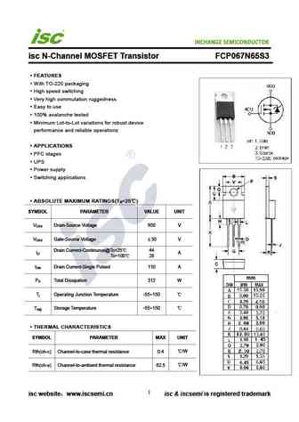
INCHANGE Semiconductor isc N-Channel MOSFET Transistor FCP067N65S3 FEATURES With TO-220 packaging High speed switching Very high commutation ruggedness Easy to use 100% avalanche tested Minimum Lot-to-Lot variations for robust device performance and reliable operationz APPLICATIONS PFC stages UPS Power supply Switching applications ABSOLUTE MAXIMUM RATIN
spw47n65c3.pdf
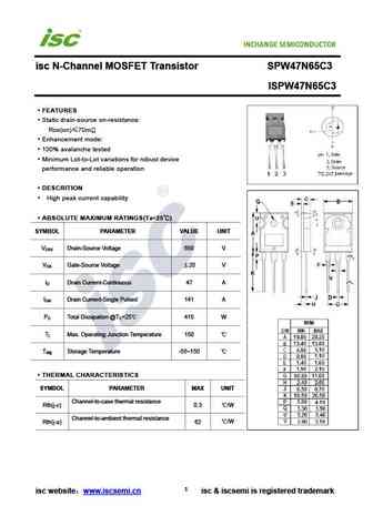
isc N-Channel MOSFET Transistor SPW47N65C3 ISPW47N65C3 FEATURES Static drain-source on-resistance RDS(on) 70m Enhancement mode 100% avalanche tested Minimum Lot-to-Lot variations for robust device performance and reliable operation DESCRITION High peak current capability ABSOLUTE MAXIMUM RATINGS(T =25 ) a SYMBOL PARAMETER VALUE UNIT V Drain-Source Voltage
spp07n65c3.pdf
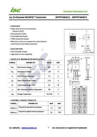
isc N-Channel MOSFET Transistor SPP07N65C3 ISPP07N65C3 FEATURES Static drain-source on-resistance RDS(on) 0.6 Enhancement mode Fast Switching Speed 100% avalanche tested Minimum Lot-to-Lot variations for robust device performance and reliable operation DESCRIPTION Ultra low gate charge High peak current capability ABSOLUTE MAXIMUM RATINGS(T =25 ) a S
fch067n65s3.pdf
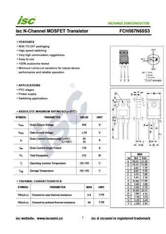
INCHANGE Semiconductor isc N-Channel MOSFET Transistor FCH067N65S3 FEATURES With TO-247 packaging High speed switching Very high commutation ruggedness Easy to use 100% avalanche tested Minimum Lot-to-Lot variations for robust device performance and reliable operation APPLICATIONS PFC stages Power supply Switching applications ABSOLUTE MAXIMUM RATINGS(T =25
aod7n65.pdf
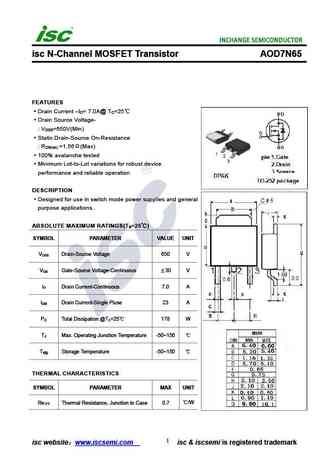
isc N-Channel MOSFET Transistor AOD7N65 FEATURES Drain Current I = 7.0A@ T =25 D C Drain Source Voltage- V =650V(Min) DSS Static Drain-Source On-Resistance R =1.56 (Max) DS(on) 100% avalanche tested Minimum Lot-to-Lot variations for robust device performance and reliable operation DESCRIPTION Designed for use in switch mode power supplies and general purpos
stw77n65m5.pdf
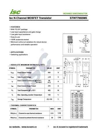
INCHANGE Semiconductor Isc N-Channel MOSFET Transistor STW77N65M5 FEATURES With TO-247 package Low input capacitance and gate charge Low gate input resistance Easy to use 100% avalanche tested Minimum Lot-to-Lot variations for robust device performance and reliable operation APPLICATIONS Switching applications ABSOLUTE MAXIMUM RATINGS(T =25 ) a SYMBOL PARAMET
dmt7n65 dmf7n65 dmk7n65 dmg7n65.pdf
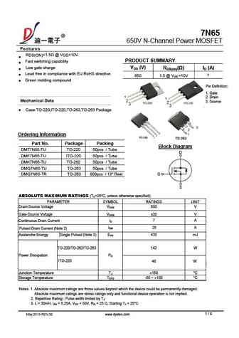
7N65 650V N-Channel Power MOSFET RDS(ON)
ap7n65f ap7n65p.pdf
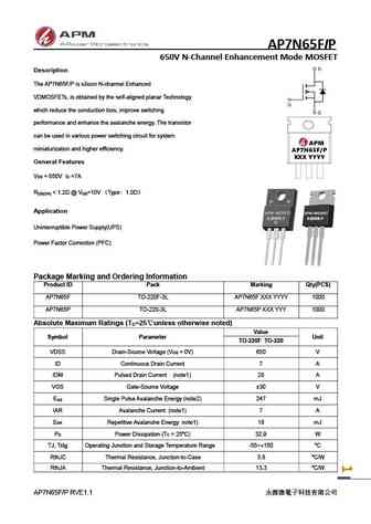
AP7N65FIP 650V N-Channel Enhancement Mode MOSFET Description The AP7N65F/P is silicon N-channel Enhanced VDMOSFETs, is obtained by the self-aligned planar Technology which reduce the conduction loss, improve switching performance and enhance the avalanche energy. The transistor can be used in various power switching circuit for system miniaturization and higher efficiency. Ge
ap7n65d ap7n65y.pdf
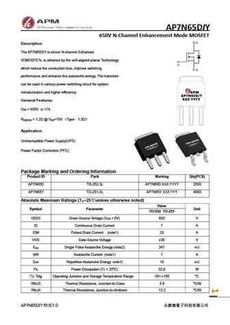
AP7N65DIY 650V N-Channel Enhancement Mode MOSFET Description The AP7N65D/Y is silicon N-channel Enhanced VDMOSFETs, is obtained by the self-aligned planar Technology which reduce the conduction loss, improve switching performance and enhance the avalanche energy. The transistor can be used in various power switching circuit for system miniaturization and higher efficiency. Ge
Другие MOSFET... 7N70 , 8N70 , 9N70 , 10N70 , 12N70 , 15N70 , 6N65Z , 7N65A , TK10A60D , 7N65Z , 7N65K , 8N65 , 9N65 , 10N65 , 10N65Z , 10N65K , 15N65 .
🌐 : EN ES РУ

Список транзисторов
Обновления
MOSFET: ASB80R750E | ASB70R380E | ASB65R300E | ASB65R220E | ASB65R120EFD | ASB60R150E | ASA80R900E | ASA80R750E | ASA80R290E | ASA70R950E | ASA70R600E | ASA70R380E | ASA70R240E | ASA65R850E | ASA65R550E | ASA65R350E
Popular searches
bc548 pinout | bdw94c | bd140 transistor | 2n2222a datasheet | bd136 | tl431 datasheet | 2sd526 | 2n4403 transistor equivalent