1N65. Аналоги и основные параметры
Наименование производителя: 1N65
Тип транзистора: MOSFET
Полярность: N
Предельные значения
Pd ⓘ - Максимальная рассеиваемая мощность: 40 W
|Vds|ⓘ - Максимально допустимое напряжение сток-исток: 650 V
|Vgs|ⓘ - Максимально допустимое напряжение затвор-исток: 30 V
|Id| ⓘ - Максимально допустимый постоянный ток стока: 1.2 A
Tj ⓘ - Максимальная температура канала: 150 °C
Электрические характеристики
tr ⓘ - Время нарастания: 25 ns
Cossⓘ - Выходная емкость: 20 pf
RDSonⓘ - Сопротивление сток-исток открытого транзистора: 9.5 Ohm
Тип корпуса: TO-220 TO-92 SOT-223 TO-126 TO-251 TO-252 TO-220F DFN-8
Аналог (замена) для 1N65
- подборⓘ MOSFET транзистора по параметрам
1N65 даташит
1n65.pdf
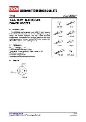
UNISONIC TECHNOLOGIES CO., LTD 1N65 Power MOSFET 1.2A, 650V N-CHANNEL POWER MOSFET 1 1 SOT-223 TO-92 DESCRIPTION The UTC 1N65 is a high voltage power MOSFET and is designed to have better characteristics, such as fast switching time, low gate 1 1 charge, low on-state resistance and high rugged avalanche TO-220 TO-220F characteristics. This power MOSFET is usually used i
1n65.pdf
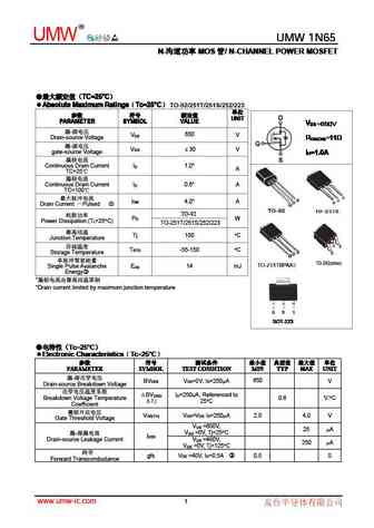
R UMW UMW 1N65 UMW 1N65 N- MOS / N-CHANNEL POWER MOSFET N- MOS / N-CHANNEL POWER MOSFET N- MOS / N-CHANNEL POWER MOSFET N- MOS / N-CHANNEL POWER MOSFET TC=25 C TC=25 C TC=25 C TC=25 C Absolute Maximum Ratings Tc=25 C Absolute Maximum Ratings Tc=25 C TO-92/251T/251S/252/223 Absolute Maximum Ratings Tc=25 C A
msjac11n65y-tp.pdf
MSJAC11N65Y Electrical Characteristics @ 25 C (Unless Otherwise Specified) Parameter Symbol Test Conditions Min Typ Max Unit Static Characteristics V(BR)DSS VGS=0V, ID=250 A Drain-Source Breakdown Voltage 650 V IGSS VDS=0V, VGS = 30V Gate-Source Leakage Current 100 nA VDS=650V, VGS=0V 1 IDSS Zero Gate Voltage Drain Current A VDS=650V, VGS=0V, TJ=150 C 100 VGS(th) VDS=
stl11n65m5.pdf
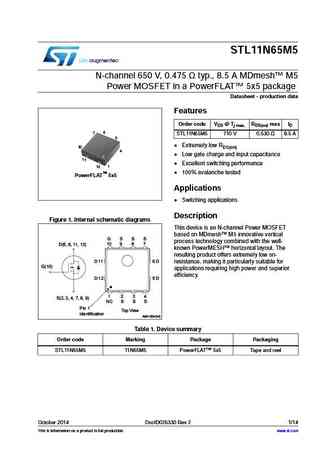
STL11N65M5 N-channel 650 V, 0.475 typ., 8.5 A MDmesh M5 Power MOSFET in a PowerFLAT 5x5 package Datasheet - production data Features Order code VDS @ Tj max. RDS(on) max ID 6 7 STL11N65M5 710 V 0.530 8.5 A 5 Extremely low RDS(on) 4 Low gate charge and input capacitance Excellent switching performance 1 12 TM 100% avalanche tested PowerFLAT 5x5
stl31n65m5.pdf
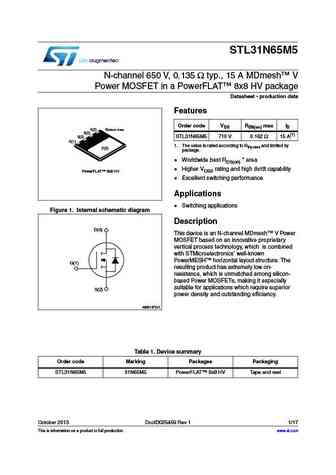
STL31N65M5 N-channel 650 V, 0.135 typ., 15 A MDmesh V Power MOSFET in a PowerFLAT 8x8 HV package Datasheet - production data Features Order code VDS RDS(on) max ID S(2) Bottom view S(2) S(2) STL31N65M5 710 V 0.162 15 A(1) G(1) 1. The value is rated according to Rthj-case and limited by D(3) package. Worldwide best RDS(on) * area Higher VDSS rating and high d
stb31n65m5 stf31n65m5 stp31n65m5 stw31n65m5.pdf
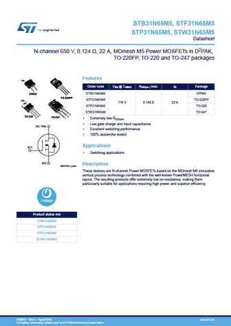
STB31N65M5, STF31N65M5 STP31N65M5, STW31N65M5 Datasheet N-channel 650 V, 0.124 , 22 A, MDmesh M5 Power MOSFETs in D2PAK, TO 220FP, TO 220 and TO-247 packages Features TAB VDS @ TJMAX RDS(on ) max. ID Order code Package 3 1 3 2 STB31N65M5 D2PAK D PAK 2 1 TO-220FP STF31N65M5 TO-220FP TAB 710 V 0.148 22 A STP31N65M5 TO-220 STW31N65M5 TO-247 3 3 2 TO-220 2 TO-24
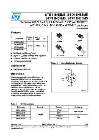
stb11n65m5 std11n65m5 stf11n65m5 stp11n65m5.pdf
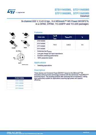
STB11N65M5, STD11N65M5 STF11N65M5, STP11N65M5 Datasheet N-channel 650 V, 0.43 typ., 9 A MDmesh M5 Power MOSFETs in a DPAK, D PAK, TO-220FP and TO-220 packages Features TAB TAB 3 2 VDS @ 3 1 1 RDS(on)max. ID Order code DPAK 2 D PAK Tjmax. TAB STB11N65M5 STD11N65M5 710 V 0.48 9 A 3 2 3 1 STF11N65M5 2 1 TO-220 TO-220FP STP11N65M5 D(2, TAB) Extremel
stb31n65m5 stf31n65m5 stfi31n65m5 stp31n65m5 stw31n65m5.pdf
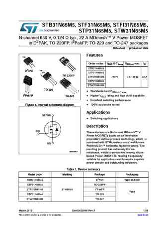
STB31N65M5, STF31N65M5, STFI31N65M5, STP31N65M5, STW31N65M5 N-channel 650 V, 0.124 typ., 22 A MDmesh V Power MOSFET in D2PAK, TO-220FP, I2PakFP, TO-220 and TO-247 packages Datasheet - production data Features TAB Order codes VDSS @ TJmax RDS(on) max ID 2 3 1 STB31N65M5 3 TAB 2 D2PAK 1 STF31N65M5 TO-220FP STFI31N65M5 710 V
std11n65m2 stp11n65m2 stu11n65m2.pdf
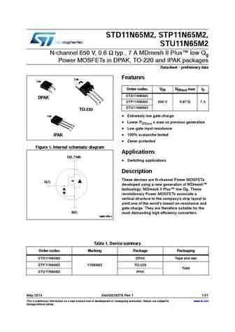
STD11N65M2, STP11N65M2, STU11N65M2 N-channel 650 V, 0.6 typ., 7 A MDmesh II Plus low Qg Power MOSFETs in DPAK, TO-220 and IPAK packages Datasheet - preliminary data Features TAB TAB 3 Order codes VDS RDS(on) max ID 1 STD11N65M2 DPAK 3 STP11N65M2 650 V 0.67 7 A 2 1 STU11N65M2 TO-220 TAB Extremely low gate charge Lower RDS(on) x area vs previous generation
stb11n65m5 stf11n65m5 stp11n65m5 stu11n65m5.pdf
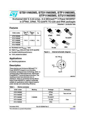
STB11N65M5, STD11N65M5, STF11N65M5, STP11N65M5, STU11N65M5 N-channel 650 V, 0.43 typ., 9 A MDmesh V Power MOSFET in D2PAK, DPAK, TO-220FP, TO-220 and IPAK packages Datasheet production data Features TAB TAB 2 VDSS @ RDS(on) 2 3 Order codes ID 3 1 TJmax max 1 3 2 DPAK D2PAK 1 STB11N65M5 TO-220FP STD11N65M5 TAB STF11N65M5 710 V
stf11n65k3.pdf
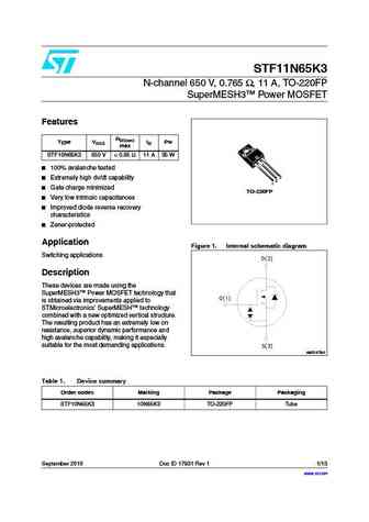
STF11N65K3 N-channel 650 V, 0.765 , 11 A, TO-220FP SuperMESH3 Power MOSFET Features RDS(on) Type VDSS ID Pw max STF10N65K3 650 V
stf11n65m2-045y.pdf
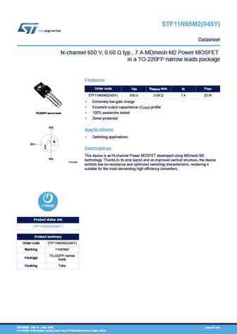
STF11N65M2(045Y) Datasheet N-channel 650 V, 0.60 typ., 7 A MDmesh M2 Power MOSFET in a TO-220FP narrow leads package Features VDS RDS(on) max. ID PTOT Order code STF11N65M2(045Y) 650 V 0.68 7 A 25 W Extremely low gate charge 3 2 1 Excellent output capacitance (COSS) profile TO-220FP narrow leads 100% avalanche tested Zener-protected D(2) Applications
std11n65m5.pdf
STB11N65M5, STD11N65M5 STF11N65M5, STP11N65M5 N-channel 650 V, 0.43 , 9 A MDmesh V Power MOSFET in D2PAK, DPAK, TO-220FP and TO-220 packages Preliminary data Features TAB TAB 2 2 3 VDSS @ RDS(on) 3 Order code ID 1 1 TJmax max DPAK D2PAK STB11N65M5 STD11N65M5 TAB 710 V
stl21n65m5.pdf
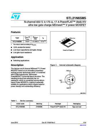
STL21N65M5 N-channel 650 V, 0.175 , 17 A PowerFLAT (8x8) HV ultra low gate charge MDmesh V power MOSFET Features VDSS @ RDS(on) Type ID S(3) Bottom iew TJmax max S(3) S(3) G(1) STL21N65M5 710 V
stf11n65m2 stf11n65m2 stfi11n65m2.pdf
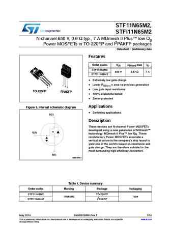
STF11N65M2, STFI11N65M2 N-channel 650 V, 0.6 typ., 7 A MDmesh II Plus low Qg Power MOSFETs in TO-220FP and I2PAKFP packages Datasheet - preliminary data Features Order codes VDS RDS(on) max ID STF11N65M2 650 V 0.67 7 A STFI11N65M2 Extremely low gate charge 3 Lower RDS(on) x area vs previous generation 1 2 2 3 1 Low gate input resistance 2 TO-220FP I P
stf11n65m2 stfi11n65m2.pdf
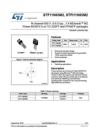
STF11N65M2, STFI11N65M2 N-channel 650 V, 0.6 typ., 7 A MDmesh M2 Power MOSFETs in TO-220FP and I PAKFP packages Datasheet - production data Features Order code V R max. I P DS DS(on) D TOT STF11N65M2 650 V 0.68 7 A 25 W STFI11N65M2 Extremely low gate charge TO-220FP I2PAKFP (TO-281) Excellent output capacitance (C ) profile OSS 100% avalanche teste
stb21n65m5 stf21n65m5 sti21n65m5 stp21n65m5 stw21n65m5.pdf
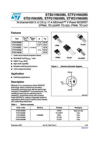
STB21N65M5, STF21N65M5 STI21N65M5, STP21N65M5, STW21N65M5 N-channel 650 V, 0.175 , 17 A MDmesh V Power MOSFET D2PAK, TO-220FP, TO-220, I2PAK, TO-247 Features VDSS @ RDS(on) Type ID PW TJmax max 3 2 3 1 STB21N65M5 17 A 125 W 2 1 TO-220 STF21N65M5 17 A(1) 30 W I PAK STI21N65M5 710 V
fch041n65f f085.pdf
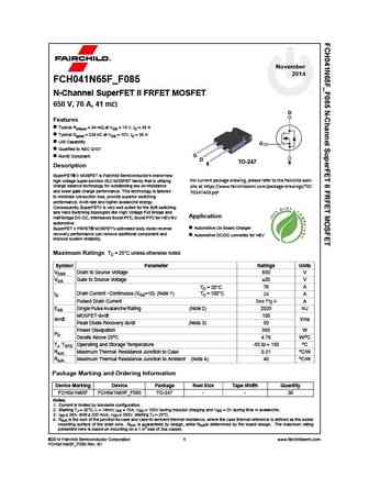
November 2014 FCH041N65F_F085 N-Channel SuperFET II FRFET MOSFET 650 V, 76 A, 41 m D Features Typical RDS(on) = 34 m at VGS = 10 V, ID = 38 A Typical Qg(tot) = 234 nC at VGS = 10V, ID = 38 A UIS Capability G Qualified to AEC Q101 G RoHS Compliant D TO-247 S S Description SuperFET II MOSFET is Fairchild Semiconductor s brand-new For current package drawing,
fch041n65f.pdf
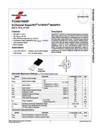
December 2014 FCH041N65F N-Channel SuperFET II FRFET MOSFET 650 V, 76 A, 41 m Features Description 700 V @ TJ = 150 C SuperFET II MOSFET is Fairchild Semiconductor s brand-new high voltage super-junction (SJ) MOSFET family that is utilizing Typ. RDS(on) = 36 m charge balance technology for outstanding low on-resistance Ultra Low Gate Charge (Typ. Qg = 226 nC
spp11n65c3 spa11n65c3 spi11n65c3 spp11n65c3 spa11n65c3 spi11n65c3 rev.2.91.pdf
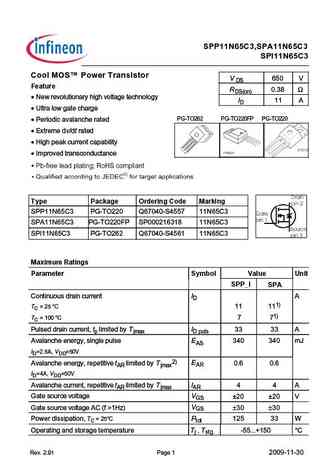
SPP11N65C3,SPA11N65C3 SPI11N65C3 Cool MOS Power Transistor V 650 V DS Feature RDS(on) 0.38 New revolutionary high voltage technology ID 11 A Ultra low gate charge PG-TO262 PG-TO220FP PG-TO220 Periodic avalanche rated Extreme dv/dt rated High peak current capability Improved transconductance Type Package Ordering Code Marking SPP11N65C3 PG-TO220 Q67
msjac11n65y.pdf

MSJAC11N65Y Electrical Characteristics @ 25 C (Unless Otherwise Specified) Parameter Symbol Test Conditions Min Typ Max Unit Static Characteristics V(BR)DSS VGS=0V, ID=250 A Drain-Source Breakdown Voltage 650 V IGSS VDS=0V, VGS = 30V Gate-Source Leakage Current 100 nA VDS=650V, VGS=0V 1 IDSS Zero Gate Voltage Drain Current A VDS=650V, VGS=0V, TJ=150 C 100 VGS(th) VDS=
msju11n65.pdf
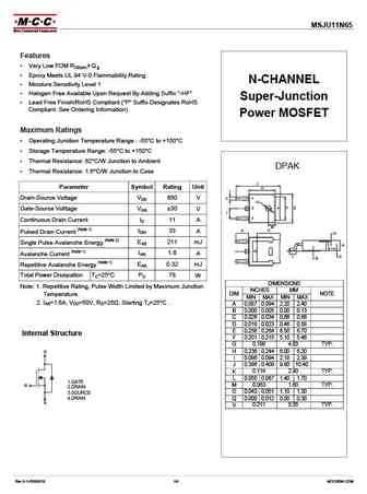
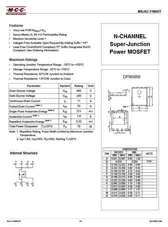
MSJU11N65 Features Very Low FOM RDS(on) Qg Epoxy Meets UL 94 V-0 Flammability Rating N-CHANNEL Moisture Sensitivity Level 1 Halogen Free Available Upon Request By Adding Suffix "-HF" Super-Junction Lead Free Finish/RoHS Compliant ("P" Suffix Designates RoHS Compliant. See Ordering Information) Power MOSFET Maximum Ratings Operating Junction Temperature Ran
fch041n65f-f085.pdf
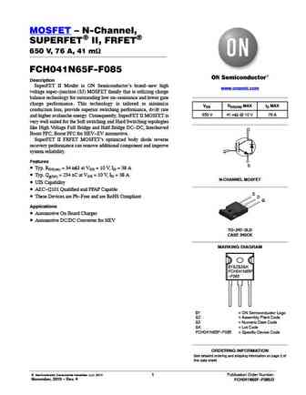
MOSFET N-Channel, SUPERFET) II, FRFET) 650 V, 76 A, 41 mW FCH041N65F-F085 Description SuperFET II Mosfet is ON Semiconductor s brand-new high www.onsemi.com voltage super-junction (SJ) MOSFET family that is utilizing charge balance technology for outstanding low on-resistance and lower gate charge performance. This technology is tailored to minimize VDS RDS(ON) MAX ID MAX condu
1n65a.pdf
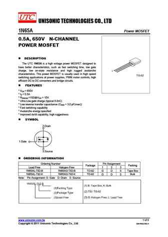
UNISONIC TECHNOLOGIES CO., LTD 1N65A Power MOSFET 0.5A, 650V N-CHANNEL POWER MOSFET DESCRIPTION The UTC 1N65A is a high voltage power MOSFET designed to have better characteristics, such as fast switching time, low gate charge, low on-state resistance and high rugged avalanche characteristics. This power MOSFET is usually used in high speed switching applications at power su
1n65l-aa3-r 1n65g-aa3-r 1n65l-ta3-t 1n65g-ta3-t 1n65l-tf3-t 1n65g-tf3-t 1n65l-tm3-t 1n65g-tm3-t 1n65l-tma-t 1n65g-tma-t.pdf
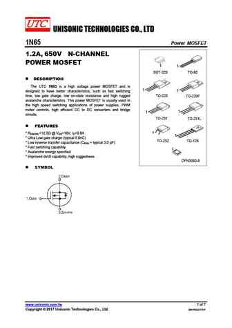
UNISONIC TECHNOLOGIES CO., LTD 1N65 Power MOSFET 1.2A, 650V N-CHANNEL POWER MOSFET 1 1 SOT-223 TO-92 DESCRIPTION The UTC 1N65 is a high voltage power MOSFET and is 1 1 designed to have better characteristics, such as fast switching time, low gate charge, low on-state resistance and high rugged TO-220 TO-220F avalanche characteristics. This power MOSFET is usually used i
1n65l-tn3-r 1n65g-tn3-r 1n65l-t60-k 1n65g-t60-k 1n65l-t92-b 1n65g-t92-b 1n65l-t92-k 1n65g-t92-k 1n65l-k08-5060-r 1n65g-k08-5060-r.pdf

UNISONIC TECHNOLOGIES CO., LTD 1N65 Power MOSFET 1.2A, 650V N-CHANNEL POWER MOSFET 1 1 SOT-223 TO-92 DESCRIPTION The UTC 1N65 is a high voltage power MOSFET and is 1 1 designed to have better characteristics, such as fast switching time, low gate charge, low on-state resistance and high rugged TO-220 TO-220F avalanche characteristics. This power MOSFET is usually used i
cjpf01n65b.pdf
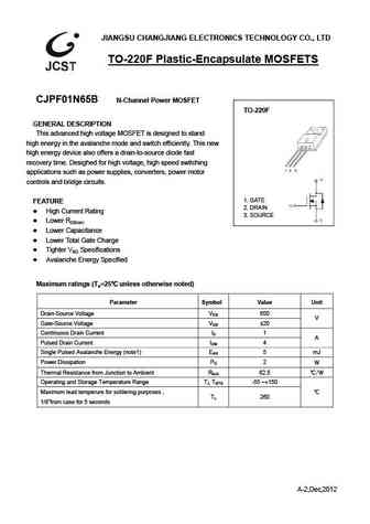
JIANGSU CHANGJIANG ELECTRONICS TECHNOLOGY CO., LTD TO-220F Plastic-Encapsulate MOSFETS CJPF01N65B N-Channel Power MOSFET TO-220F GENERAL DESCRIPTION This advanced high voltage MOSFET is designed to stand high energy in the avalanche mode and switch efficiently. This new high energy device also offers a drain-to-source diode fast recovery time. Desighed for high voltage, high
cjv01n65b.pdf
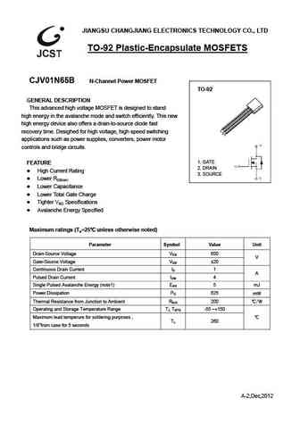
JIANGSU CHANGJIANG ELECTRONICS TECHNOLOGY CO., LTD TO-92 Plastic-Encapsulate MOSFETS CJV01N65B N-Channel Power MOSFET TO-92 GENERAL DESCRIPTION This advanced high voltage MOSFET is designed to stand high energy in the avalanche mode and switch efficiently. This new high energy device also offers a drain-to-source diode fast recovery time. Desighed for high voltage, high speed
cju01n65b.pdf

JIANGSU CHANGJIANG ELECTRONICS TECHNOLOGY CO., LTD TO-252-2L Plastic-Encapsulate MOSFETS CJU01N65B N-Channel Power MOSFET TO-252-2L GENERAL DESCRIPTION This advanced high voltage MOSFET is designed to stand high energy in the avalanche mode and switch efficiently. This new high energy device also offers a drain-to-source diode fast recovery time. Desighed for high voltage, hi
cjb01n65b.pdf
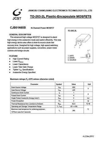
JIANGSU CHANGJIANG ELECTRONICS TECHNOLOGY CO., LTD TO-263-2L Plastic-Encapsulate MOSFETS CJB01N65B N-Channel Power MOSFET TO-263-2L GENERAL DESCRIPTION This advanced high voltage MOSFET is designed to stand high energy in the avalanche mode and switch efficiently. This new high energy device also offers a drain-to-source diode fast recovery time. Desighed for high voltage, hi
cjd01n65b.pdf
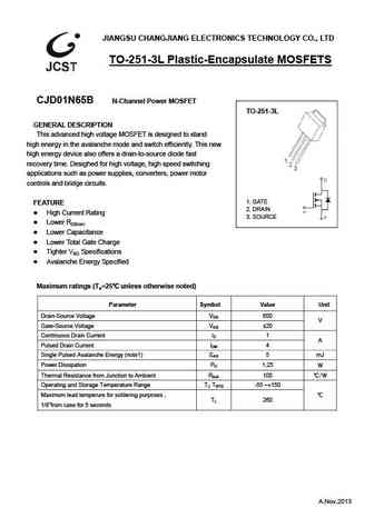
JIANGSU CHANGJIANG ELECTRONICS TECHNOLOGY CO., LTD TO-251-3L Plastic-Encapsulate MOSFETS CJD01N65B N-Channel Power MOSFET TO-251-3L GENERAL DESCRIPTION This advanced high voltage MOSFET is designed to stand high energy in the avalanche mode and switch efficiently. This new high energy device also offers a drain-to-source diode fast recovery time. Desighed for high voltage, hi
cjp01n65b.pdf

JIANGSU CHANGJIANG ELECTRONICS TECHNOLOGY CO., LTD TO-220-3L Plastic-Encapsulate MOSFETS CJP01N65B N-Channel Power MOSFET TO-220-3L GENERAL DESCRIPTION This advanced high voltage MOSFET is designed to stand high energy in the avalanche mode and switch efficiently. This new high energy device also offers a drain-to-source diode fast recovery time. Desighed for high voltage, hi
ceu01n65a ced01n65a.pdf
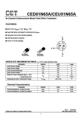
CED01N65A/CEU01N65A N-Channel Enhancement Mode Field Effect Transistor FEATURES 650V, 0.9A, RDS(ON) = 15 @VGS = 10V. Super high dense cell design for extremely low RDS(ON). High power and current handing capability. D Lead free product is acquired. TO-251 & TO-252 package. G D G S CEU SERIES CED SERIES TO-252(D-PAK) TO-251(I-PAK) S ABSOLUTE MAXIMUM RATINGS Tc = 25 C unless
ceu01n65 ced01n65.pdf
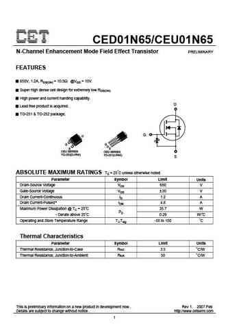
CED01N65/CEU01N65 N-Channel Enhancement Mode Field Effect Transistor PRELIMINARY FEATURES 650V, 1.2A, RDS(ON) = 10.5 @VGS = 10V. Super high dense cell design for extremely low RDS(ON). High power and current handing capability. D Lead free product is acquired. TO-251 & TO-252 package. G D G S CEU SERIES CED SERIES TO-252(D-PAK) TO-251(I-PAK) S ABSOLUTE MAXIMUM RATINGS Tc =
cek01n65a.pdf
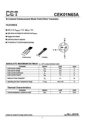
CEK01N65A N-Channel Enhancement Mode Field Effect Transistor FEATURES 650V, 0.3A, RDS(ON) = 15 @VGS = 10V. High dense cell design for extremely low RDS(ON). Rugged and reliable. D Lead free product is acquired. TO-92(Bulk) & TO-92(Ammopack) package. G G D G S D S TO-92(Ammopack) TO-92(Bulk) S ABSOLUTE MAXIMUM RATINGS TA = 25 C unless otherwise noted Parameter Symbol Limit
cek01n65.pdf
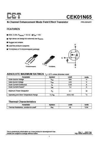
CEK01N65 PRELIMINARY N-Channel Enhancement Mode Field Effect Transistor FEATURES 650V, 0.35A, RDS(ON) = 10.5 @VGS = 10V. High dense cell design for extremely low RDS(ON). Rugged and reliable. D Lead free product is acquired. TO-92(Bulk) & TO-92(Ammopack) package. G G D G S D S TO-92(Ammopack) TO-92(Bulk) S ABSOLUTE MAXIMUM RATINGS TA = 25 C unless otherwise noted Paramet
cep01n65 ceb01n65 cef01n65.pdf
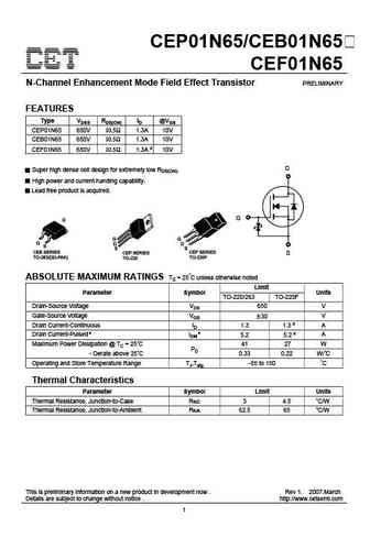
CEP01N65/CEB01N65 CEF01N65 N-Channel Enhancement Mode Field Effect Transistor PRELIMINARY FEATURES Type VDSS RDS(ON) ID @VGS CEP01N65 650V 10.5 1.3A 10V CEB01N65 650V 10.5 1.3A 10V CEF01N65 650V 10.5 1.3A d 10V D Super high dense cell design for extremely low RDS(ON). High power and current handing capability. Lead free product is acquired. G CEB SERIES CEP SERIES CEF SE
sif1n65c.pdf
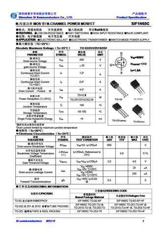
Shenzhen SI Semiconductors Co., LTD. Product Specification Shenzhen SI Semiconductors Co., LTD. Product Specification Shenzhen SI Semiconductors Co., LTD. Product Specification Shenzhen SI Semiconductors Co., LTD. Product Specification N- MOS / N-CHANNEL POWER MOSFET SIF1N65C N- MOS / N-CHANNEL POWER MOSFET SIF1N65C N- MOS / N-CHANN
mtn1n65i3.pdf
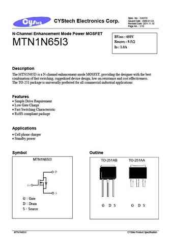
Spec. No. C437I3 Issued Date 2009.01.23 CYStech Electronics Corp. Revised Date 2011.11.10 Page No. 1/10 N-Channel Enhancement Mode Power MOSFET BVDSS 650V RDS(ON) 9.5 MTN1N65I3 ID 1.0A Description The MTN1N65I3 is a N-channel enhancement-mode MOSFET, providing the designer with the best combination of fast switching, ruggedized device design, low on-resista
gc11n65t gc11n65f gc11n65k.pdf
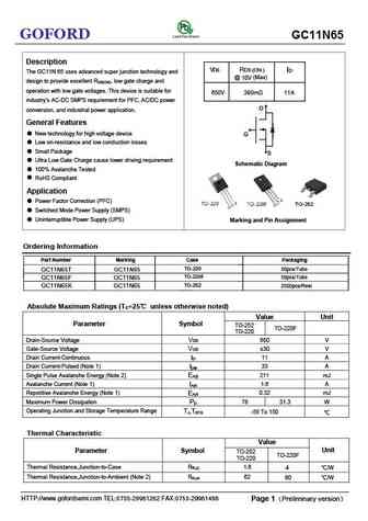
GC11N65 GOFORD Description VDS RDS (ON ) ID The GC11N 65 uses advanced super junction technology and @ (Max) 10V design to provide excellent R , low gate charge and DS(ON) operation with low gate voltages. This device is suitable for 650V 360m 11 A industry s AC-DC SMPS requirement for PFC, AC/DC power conversion, and industrial power application. General F
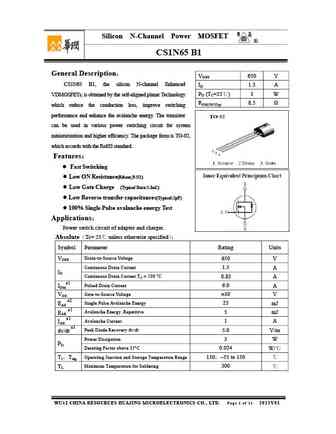
cs1n65 a1.pdf
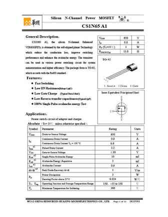
Silicon N-Channel Power MOSFET R CS1N65 A1 General Description VDSS 650 V CS1N65 A1, the silicon N-channel Enhanced ID 0.8 A PD (TC=25 ) 3 W VDMOSFETs, is obtained by the self-aligned planar Technology RDS(ON)Typ 13.8 which reduce the conduction loss, improve switching performance and enhance the avalanche energy. The transistor can be used in various power s
cs1n65 b1.pdf

Silicon N-Channel Power MOSFET R CS1N65 B1 General Description VDSS 650 V CS1N65 B1, the silicon N-channel Enhanced ID 1.5 A PD (TC=25 ) 3 W VDMOSFETs, is obtained by the self-aligned planar Technology RDS(ON)Typ 8.5 which reduce the conduction loss, improve switching performance and enhance the avalanche energy. The transistor can be used in various power s
cs1n65 b3.pdf
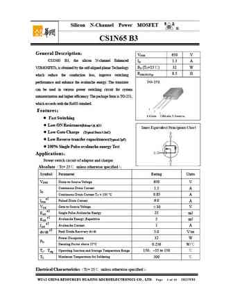
Silicon N-Channel Power MOSFET R CS1N65 B3 General Description VDSS 650 V CS1N65 B3, the silicon N-channel Enhanced ID 1.5 A PD (TC=25 ) 32 W VDMOSFETs, is obtained by the self-aligned planar Technology RDS(ON)Typ 8.5 which reduce the conduction loss, improve switching performance and enhance the avalanche energy. The transistor can be used in various power s
cs1n65 a3.pdf
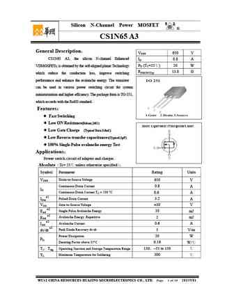
Silicon N-Channel Power MOSFET R CS1N65 A3 General Description VDSS 650 V CS1N65 A3, the silicon N-channel Enhanced ID 0.8 A PD (TC=25 ) 20 W VDMOSFETs, is obtained by the self-aligned planar Technology RDS(ON)Typ 13.8 which reduce the conduction loss, improve switching performance and enhance the avalanche energy. The transistor can be used in various power
dhsj11n65 dhfsj11n65 dhisj11n65 dhesj11n65 dhbsj11n65 dhdsj11n65.pdf
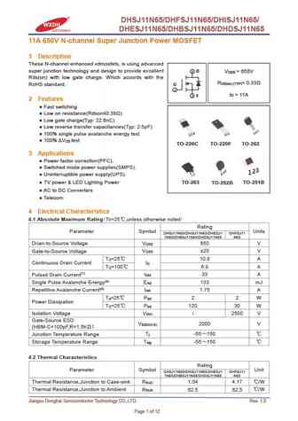
DHSJ11N65/DHFSJ11N65/DHISJ11N65/ DHESJ11N65/DHBSJ11N65/DHDSJ11N65 11A 650V N-channel Super Junction Power MOSFET 1 Description These N-channel enhanced vdmosfets, is using advanced super junction technology and design to provide excellent 2 D V = 650V DSS Rds(on) with low gate charge. Which accords with the R = 0.33 DS(on) (TYP) RoHS standard. G 1 I = 11A 3 S D 2 Features
dhsj21n65z.pdf
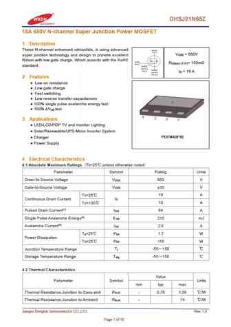
DHSJ21N65Z 16A 650V N-channel Super Junction Power MOSFET 1 Description These N-channel enhanced vdmosfets, is using advanced V = 650V DSS super junction technology and design to provide excellent Rdson with low gate charge. Which accords with the RoHS R = 150m DS(on) (TYP) standard. I = 16 A D 2 Features Low on resistance Low gate charge Fast switching Low re
dhsj21n65w.pdf
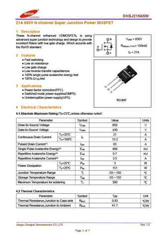
DHSJ21N65W 21A 650V N-channel Super Junction Power MOSFET 1 Description These N-channel enhanced VDMOSFETs, is using 2 D V = 650V DSS advanced super junction technology and design to provide excellent Rdson with low gate charge. Which accords with R = 150m DS(on) (TYP) G the RoHS standard. 1 I = 21A 3 S D 2 Features Fast switching Low on resistance
svsp11n65dd2tra svsp11n65fd2 svsp11n65sd2 svsp11n65sd2tr svsp11n65fjdd2 svsp11n65kd2 svsp11n65td2.pdf
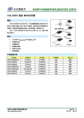
SVSP11N65D/F/S/FJD/K/TD2 11A, 650V MOS 2 1 SVSP11N65D/F/S/FJD/K/TD2 N MOSFET 3 1 TO-263-2L MOS 3 1. 2. 3. S
svsp11n65fjhd2.pdf
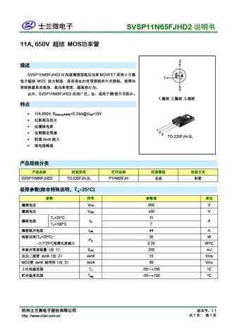
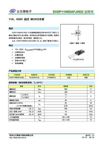
SVSP11N65FJHD2 11A, 650V MOS 2 SVSP11N65FJHD2 N MOSFET 1 MOS 3 SVSP11N65FJHD2 / 1.
svs11n65dd2tr svs11n65fd2 svs11n65sd2 svs11n65sd2tr svs11n65fjd2.pdf
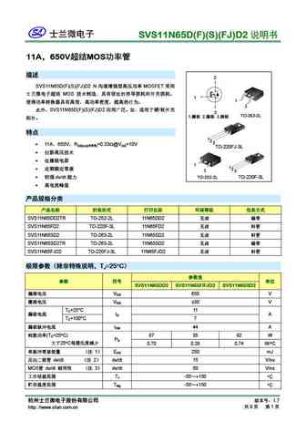
SVS11N65D(F)(S)(FJ)D2 11A 650V MOS 2 SVS11N65D(F)(S)(FJ)D2 N MOSFET MOS 1 1 3 SVS11N65D(F)(S)(FJ)D2
svs11n65fjd2.pdf
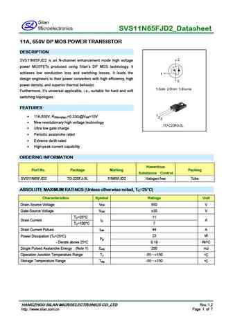
SVS11N65FJD2_Datasheet 11A, 650V DP MOS POWER TRANSISTOR DESCRIPTION SVS11N65FJD2 is an N-channel enhancement mode high voltage power MOSFETs produced using Silan s DP MOS technology. It achieves low conduction loss and switching losses. It leads the design engineers to their power converters with high efficiency, high power density, and superior thermal behavior. Furthermore,
mdf11n65b.pdf
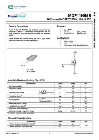
MDF11N65B N-Channel MOSFET 650V, 12A, 0.65 General Description Features These N-channel MOSFET are produced using advanced VDS = 650V MagnaChip s MOSFET Technology, which provides low on- ID = 12A @ VGS = 10V state resistance, high switching performance and excellent RDS(ON) 0.65 @ VGS = 10V quality. Applications These devices are suitable device for SMPS, high Speed
mdf11n65bth.pdf

MDF11N65B N-Channel MOSFET 650V, 12A, 0.65 General Description Features These N-channel MOSFET are produced using advanced VDS = 650V MagnaChip s MOSFET Technology, which provides low on- ID = 12A @ VGS = 10V state resistance, high switching performance and excellent RDS(ON) 0.65 @ VGS = 10V quality. Applications These devices are suitable device for SMPS, high Speed
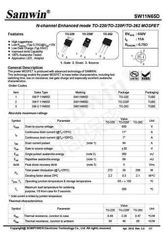
swp11n65d swf11n65d swu11n65d.pdf
SW11N65D N-channel Enhanced mode TO-220/TO-220F/TO-262 MOSFET TO-220 TO-220F TO-262 BVDSS 650V Features ID 11A High ruggedness RDS(ON) 0.75 Low RDS(ON) (Typ 0.75 )@VGS=10V Low Gate Charge (Typ 43nC) 2 Improved dv/dt Capability 1 1 1 100% Avalanche Tested 2 2 1 2 3 3 3 Application LED , Adaptor 1. Gate 2. Drain 3. Source
src11n65.pdf
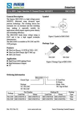
Datasheet 11A, 650V, Super Junction N-Channel Power MOSFET SRC11N65 General Description Symbol The Sanrise SRC11N65 is a high voltage power MOSFET, fabricated using advanced super junction technology. The resulting device has extremely low on resistance and fast switching time, making it especially suitable for applications which require superior power density and outstanding ef
hfd1n65s.pdf
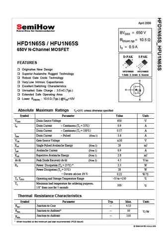
April 2009 BVDSS = 650 V RDS(on) typ HFD1N65S / HFU1N65S ID = 0.9 A 650V N-Channel MOSFET D-PAK I-PAK 2 FEATURES 1 1 3 2 3 Originative New Design HFD1N65S HFU1N65S Superior Avalanche Rugged Technology 1.Gate 2. Drain 3. Source Robust Gate Oxide Technology D Very Low Intrinsic Capacitances Excellent Switching Characteristics G Unrivalled Gate Charge
hfb1n65s.pdf
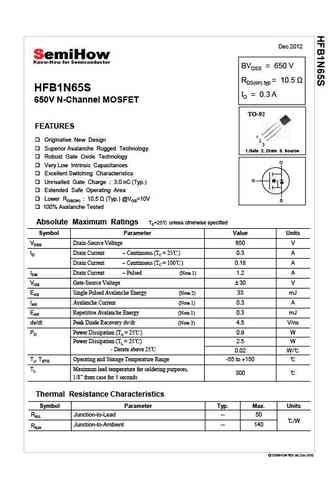
Dec 2012 BVDSS = 650 V RDS(on) typ HFB1N65S ID = 0.3 A 650V N-Channel MOSFET TO-92 FEATURES 1 Originative New Design 2 3 Superior Avalanche Rugged Technology 1.Gate 2. Drain 3. Source Robust Gate Oxide Technology D Very Low Intrinsic Capacitances Excellent Switching Characteristics G Unrivalled Gate Charge 3.0 nC (Typ.) Extended Safe Operating Area
sl11n65cf sl11n65c sl11n65ck.pdf

SL11N65C N-Channel Super Junction Power MOSFET V 650 V DS Features R 300 m DS(ON)TYP New technology for high voltage device ID 11.5 A Low on-resistance and low conduction losses small package Ultra Low Gate Charge cause lower driving requirements 100% Avalanche Tested ROHS compliant Application Power factor correction PFC Swit
sl11n65c.pdf
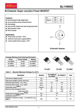
SL11N65C N-Channel Super Junction Power MOSFET V 650 V DS Features R 300 m DS(ON)TYP New technology for high voltage device ID 11.5 A Low on-resistance and low conduction losses small package Ultra Low Gate Charge cause lower driving requirements 100% Avalanche Tested ROHS compliant Application Power factor correction PFC Swit
sl21n65c.pdf
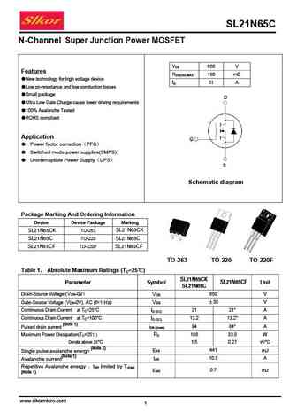
SL21N65C N-Channel Super Junction Power MOSFET V 650 V DS Features R 180 m DS(ON) MAX New technology for high voltage device ID 21 A Low on-resistance and low conduction losses Small package Ultra Low Gate Charge cause lower driving requirements 100% Avalanche Tested ROHS compliant Application Power factor correction PFC Switched mo
qm01n65u.pdf
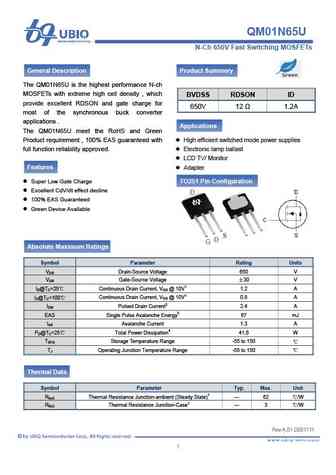
QM01N65U 1 2011-05-25 - 1 - N-Ch 650V Fast Switching MOSFETs General Description Product Summery The QM01N65U is the highest performance N-ch MOSFETs with extreme high cell density , which BVDSS RDSON ID provide excellent RDSON and gate charge for 650V 12 1.2A most of the synchronous buck converter applications . Applications The QM01N65U meet the RoHS and
qm01n65l.pdf
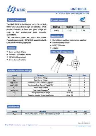
QM01N65L 1 2011-06-15 - 1 - N-Ch 650V Fast Switching MOSFETs General Description Product Summery The QM01N65L is the highest performance N-ch MOSFETs with extreme high cell density , which BVDSS RDSON ID provide excellent RDSON and gate charge for 650V 12 0.2A most of the synchronous buck converter applications . Applications The QM01N65L meet the RoHS and
qm01n65d.pdf
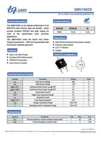
QM01N65D 1 2011-06-22 - 1 - N-Ch 650V Fast Switching MOSFETs General Description Product Summery The QM01N65D is the highest performance N-ch MOSFETs with extreme high cell density , which BVDSS RDSON ID provide excellent RDSON and gate charge for 650V 12 1.2A most of the synchronous buck converter applications . Applications The QM01N65D meet the RoHS and
wml11n65sr wmk11n65sr wmm11n65sr wmn11n65sr wmp11n65sr wmo11n65sr.pdf
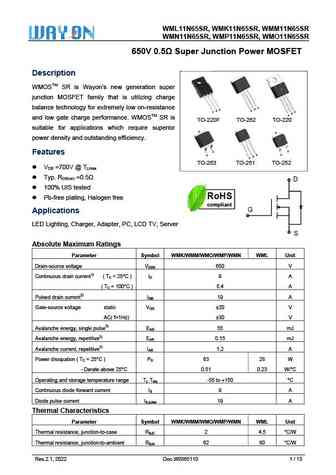
WML11N65SR, W 65SR, WM SR WMK11N6 MM11N65S WMN11N65SR, WMP11N6 MO11N65S 65SR, WM SR 650V 0.5 Su nction P uper Jun Power MOSFET Descrip ption WMOSTM SR is Wa new generation super ayon s w junction MOSFET fa that is utilizing charge M amily S balance te or extremely esistance echnology fo y low on-re D S D G G G S D G T and low ga charge performanc W
cs1n65a3.pdf

Silicon N-Channel Power MOSFET R CS1N65 A3 General Description VDSS 650 V CS1N65 A3, the silicon N-channel Enhanced ID 0.8 A PD (TC=25 ) 20 W VDMOSFETs, is obtained by the self-aligned planar Technology RDS(ON)Typ 13.8 which reduce the conduction loss, improve switching performance and enhance the avalanche energy. The transistor can be used in various power
cs1n65b1.pdf
Silicon N-Channel Power MOSFET R CS1N65 B1 General Description VDSS 650 V CS1N65 B1, the silicon N-channel Enhanced ID 1.5 A PD (TC=25 ) 3 W VDMOSFETs, is obtained by the self-aligned planar Technology RDS(ON)Typ 8.5 which reduce the conduction loss, improve switching performance and enhance the avalanche energy. The transistor can be used in various power s
cs1n65b3.pdf

Silicon N-Channel Power MOSFET R CS1N65 B3 General Description VDSS 650 V CS1N65 B3, the silicon N-channel Enhanced ID 1.5 A PD (TC=25 ) 32 W VDMOSFETs, is obtained by the self-aligned planar Technology RDS(ON)Typ 8.5 which reduce the conduction loss, improve switching performance and enhance the avalanche energy. The transistor can be used in various power s
cs1n65a1.pdf

Silicon N-Channel Power MOSFET R CS1N65 A1 General Description VDSS 650 V CS1N65 A1, the silicon N-channel Enhanced ID 0.8 A PD (TC=25 ) 3 W VDMOSFETs, is obtained by the self-aligned planar Technology RDS(ON)Typ 13.8 which reduce the conduction loss, improve switching performance and enhance the avalanche energy. The transistor can be used in various power s
cs11n65f cs11n65p.pdf
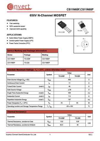
nvert Suzhou Convert Semiconductor Co ., Ltd. CS11N65F,CS11N65P 650V N-Channel MOSFET FEATURES Fast switching 100% avalanche tested Improved dv/dt capability APPLICATIONS Switch Mode Power Supply (SMPS) Uninterruptible Power Supply (UPS) Power Factor Correction (PFC) Device Marking and Package Information Device Package Marking CS11N65F TO-220F CS11N65F CS
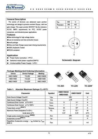
hms11n65k hms11n65i.pdf
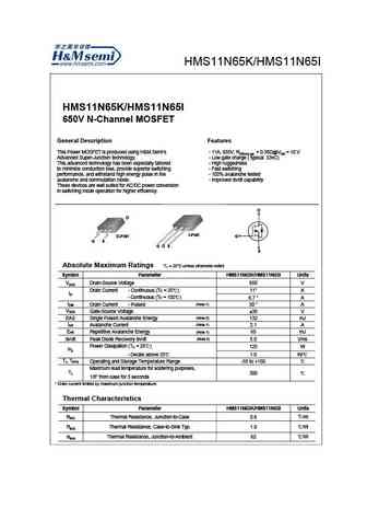
HMS11N65K/HMS11N65I HMS11N65K/HMS11N65I 650V N-Channel MOSFET General Description Features This Power MOSFET is produced using H&M Semi s - 11A, 650V, RDS(on) typ. = 0.38 @VGS = 10 V Advanced Super-Junction technology. - Low gate charge ( typical 33nC) This advanced technology has been especially tailored - High ruggedness to minimize conduction loss, provide superior switching - Fast
hms11n65i hms11n65k.pdf
HMS11N65I / HMS11N65K N-Channel Super Junction Power MOSFET General Description The series of devices use advanced trench gate super V 650 V DS junction technology and design to provide excellent RDS(ON) R 290 m DS(ON)TYP with low gate charge. This super junction MOSFET fits the ID 11.5 A industry s AC-DC SMPS requirements for PFC, AC/DC power conversion, and industri
hms21n65a.pdf
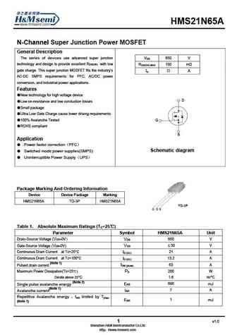
HMS21N65A N-Channel Super Junction Power MOSFET General Description The series of devices use advanced super junction VDS 650 V technology and design to provide excellent RDS(ON) with low RDS(ON) MAX 180 m gate charge. This super junction MOSFET fits the industry s ID 21 A AC-DC SMPS requirements for PFC, AC/DC power conversion, and industrial power applications. Features
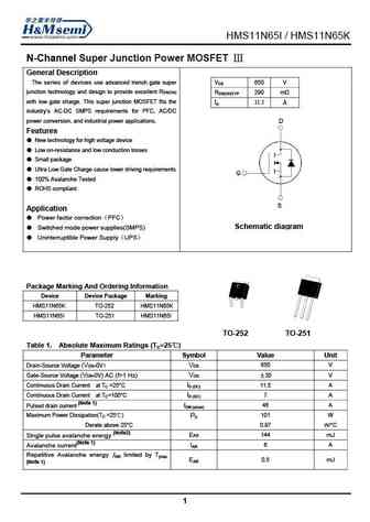
hms11n65 hms11n65d hms11n65f.pdf
HMS11N65/ HMS11N65F/HMS11N65D General Description The series of devices use advanced super junction VDS 650 V technology and design to provide excellent RDS(ON) with low RDS(ON)MAX 360 m gate charge. This super junction MOSFET fits the industry s ID 11 A AC-DC SMPS requirements for PFC, AC/DC power conversion, and industrial power applications. Features New technology
hms21n65 hms21n65f.pdf
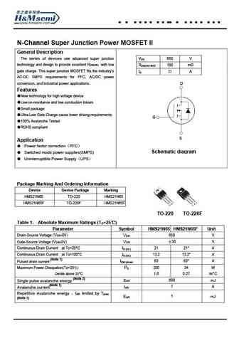
HMS21N65,HMS21N65F N-Channel Super Junction Power MOSFET II General Description The series of devices use advanced super junction VDS 650 V technology and design to provide excellent RDS(ON) with low RDS(ON) MAX 180 m gate charge. This super junction MOSFET fits the industry s ID 21 A AC-DC SMPS requirements for PFC, AC/DC power conversion, and industrial power applications
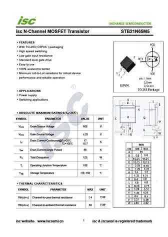
stb31n65m5.pdf
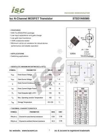
Isc N-Channel MOSFET Transistor STB31N65M5 FEATURES With To-263(D2PAK) package Low input capacitance and gate charge Low gate input resistance 100% avalanche tested Minimum Lot-to-Lot variations for robust device performance and reliable operation APPLICATIONS Switching applications ABSOLUTE MAXIMUM RATINGS(T =25 ) a SYMBOL PARAMETER VALUE UNIT V Drain-Source Vo
stp11n65m5.pdf
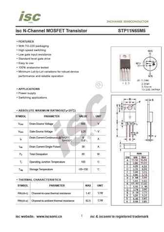
isc N-Channel MOSFET Transistor STP11N65M5 FEATURES With TO-220 packaging High speed switching Low gate input resistance Standard level gate drive Easy to use 100% avalanche tested Minimum Lot-to-Lot variations for robust device performance and reliable operation APPLICATIONS Power supply Switching applications ABSOLUTE MAXIMUM RATINGS(T =25 ) a SYMBOL P
stb21n65m5.pdf
INCHANGE Semiconductor isc N-Channel MOSFET Transistor STB21N65M5 FEATURES With TO-263( D2PAK ) packaging High speed switching Low gate input resistance Standard level gate drive Easy to use 100% avalanche tested Minimum Lot-to-Lot variations for robust device performance and reliable operation APPLICATIONS Power supply Switching applications ABSOLUTE MAXIM
spp11n65c3.pdf
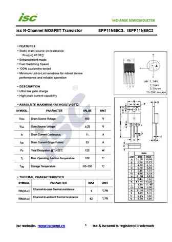
isc N-Channel MOSFET Transistor SPP11N65C3 ISPP11N65C3 FEATURES Static drain-source on-resistance RDS(on) 0.38 Enhancement mode Fast Switching Speed 100% avalanche tested Minimum Lot-to-Lot variations for robust device performance and reliable operation DESCRIPTION Ultra low gate charge High peak current capability ABSOLUTE MAXIMUM RATINGS(T =25 ) a
11n65gs.pdf
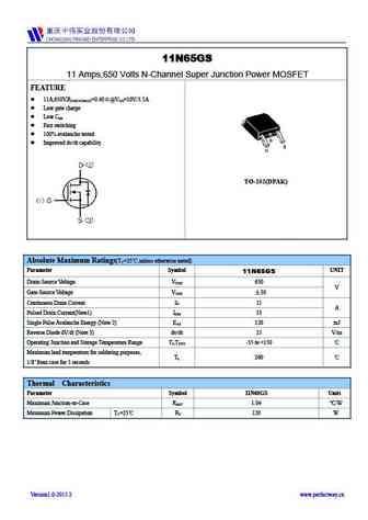
11N65GS 11 Amps,650 Volts N-Channel Super Junction Power MOSFET FEATURE 11A,650V,R =0.40 @V =10V/5.5A DS(ON)MAX GS Low gate charge Low C iss Fast switching 100% avalanche tested Improved dv/dt capability TO-252(DPAK) Absolute Maximum Ratings(T =25 ,unless otherwise noted) C Parameter Symbol UNIT 11N65GS Drain-Source Voltage V 650 DSS V Gate-Source V
11n65tfs.pdf
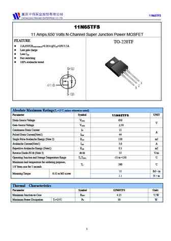
11N65TFS 11N65TFS 11 Amps,650 Volts N-Channel Super Junction Power MOSFET FEATURE TO-220TF 11A,650V,R =0.36 @V =10V/5.5A DS(ON)MAX GS Low gate charge Low C iss Fast switching 100% avalanche tested Absolute Maximum Ratings(T =25 ,unless otherwise noted) C Parameter Symbol UNIT 11N65TFS Drain-Source Voltage V 650 DSS V Gate-Source Voltage V 30 GSS Con
Другие MOSFET... 10N65 , 10N65Z , 10N65K , 15N65 , 18N65 , 20N65 , 22N65 , 1N65A , 20N50 , 2N65 , 2N65L , 2N65Z , 2N65K , 3N65A , 3N65 , 3N65Z , 3N65K .
History: 2SK3462
History: 2SK3462
🌐 : EN ES РУ

Список транзисторов
Обновления
MOSFET: 2N7002KM | 2N7002KH | AON5802 | AOSS62934 | AOSN21319C | AONS66966 | AONR62992 | AON7400B | AON6578 | AO3480C | AO3400C | HAF1008S | HAF1008L | EMZB08P03H | CS30N20FA9R | AOT66613L
Popular searches
2sc458 transistors | 2sa992 | 2sa970 | a970 | d2390 transistor | 2n5087 equivalent | tip147 datasheet | 2n4124