2N65 datasheet, аналоги, основные параметры
Наименование производителя: 2N65 📄📄
Тип транзистора: MOSFET
Полярность: N
Предельные значения
Pd ⓘ - Максимальная рассеиваемая мощность: 40 W
|Vds|ⓘ - Максимально допустимое напряжение сток-исток: 650 V
|Vgs|ⓘ - Максимально допустимое напряжение затвор-исток: 30 V
|Id| ⓘ - Максимально допустимый постоянный ток стока: 2 A
Tj ⓘ - Максимальная температура канала: 150 °C
Электрические характеристики
tr ⓘ - Время нарастания: 40 ns
Cossⓘ - Выходная емкость: 40 pf
RDSonⓘ - Сопротивление сток-исток открытого транзистора: 3.9 Ohm
📄📄 Копировать
Аналог (замена) для 2N65
- подборⓘ MOSFET транзистора по параметрам
2N65 даташит
2n65.pdf
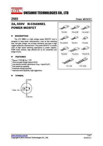
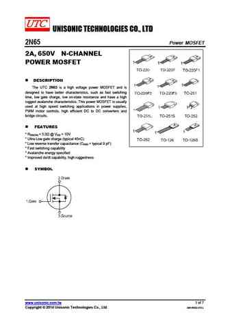
UNISONIC TECHNOLOGIES CO., LTD 2N65 Power MOSFET 2A, 650V N-CHANNEL POWER MOSFET DESCRIPTION The UTC 2N65 is a high voltage power MOSFET and is designed to have better characteristics, such as fast switching time, low gate charge, low on-state resistance and have a high rugged avalanche characteristics. This power MOSFET is usually used at high speed switching applications
2n65.pdf
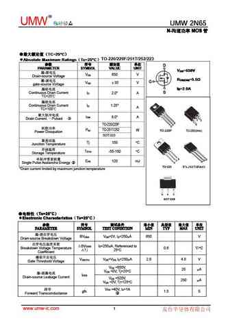
R UMW UMW 2N65 UMW 2N65 N- MOS N- MOS N- MOS N- MOS TC=25 C TC=25 C TC=25 C TC=25 C TO-220/220F/251T/252/223 Absolute Maximum Ratings Tc=25 C Absolute Maximum Ratings Tc=25 C Absolute Maximum Ratings Tc=25 C Absolute Maximum Ratings Tc=25 C PARAMETER SYMBOL VALUE U
2n65 2n65f 2n65e 2n65d 2n65n 2n65m.pdf
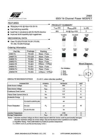
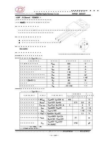
R 2N65 S E M I C O N D U C T O R 650V N-Channel Power MOSFET FEATURES PRODUCT SUMMARY RDS(ON)
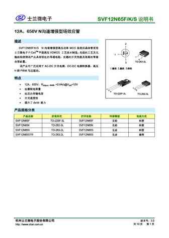
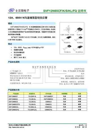
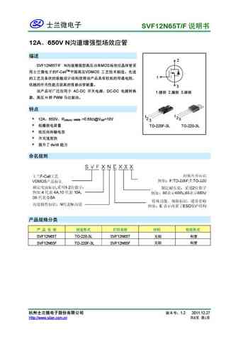
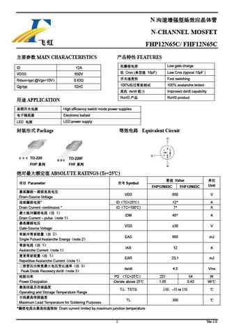
svf12n65f svf12n65t.pdf
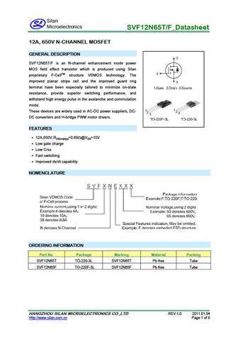
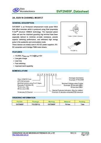
SVF12N65T/F_Datasheet 12A, 650V N-CHANNEL MOSFET GENERAL DESCRIPTION SVF12N65T/F is an N-channel enhancement mode power MOS field effect transistor which is produced using Silan proprietary F-CellTM structure VDMOS technology. The improved planar stripe cell and the improved guard ring terminal have been especially tailored to minimize on-state resistance, provide superior switch
fqp12n65c fqpf12n65c.pdf
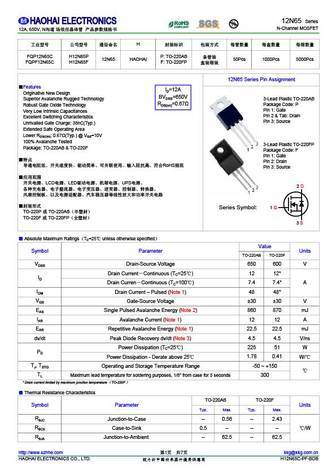
12N65 Series N-Channel MOSFET 12A, 650V, N H FQP12N65C H12N65P P TO-220AB 12N65 HAOHAI 50Pcs 1000Pcs 5000Pcs FQPF12N65C H12N65F F TO-220FP 12N65 Series Pin Assignment Features ID=12A Originative New Des
jcs12n65t.pdf
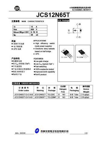
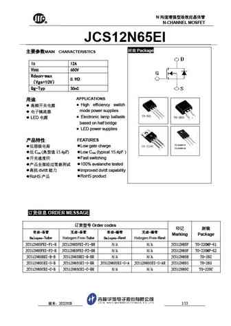
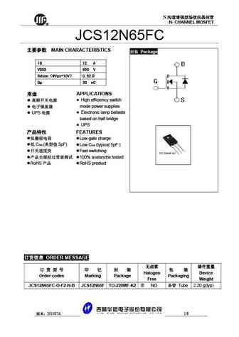
N R N-CHANNEL MOSFET JCS12N65T Package MAIN CHARACTERISTICS ID 12 A VDSS 650 V Rdson @Vgs=10V 0.78 Qg 39 nC APPLICATIONS High efficiency switch mode power supplies Electronic lamp ballasts UPS based on half bridge UPS FEA
cef02n65d cep02n65d ceb02n65d.pdf
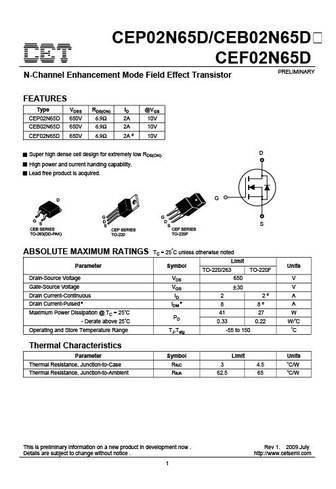
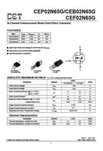
CEP02N65D/CEB02N65D CEF02N65D PRELIMINARY N-Channel Enhancement Mode Field Effect Transistor FEATURES Type VDSS RDS(ON) ID @VGS CEP02N65D 650V 6.9 2A 10V CEB02N65D 650V 6.9 2A 10V CEF02N65D 650V 6.9 2A d 10V D Super high dense cell design for extremely low RDS(ON). High power and current handing capability. Lead free product is acquired. G S CEB SERIES CEP SERIES CEF S
12n65kl-t 12n65kg-t.pdf

UNISONIC TECHNOLOGIES CO., LTD 12N65K-MT Power MOSFET 12A, 650V N-CHANNEL POWER MOSFET DESCRIPTION The UTC 12N65K-MT are N-Channel enhancement mode power field effect transistors (MOSFET) which are produced by using UTC s proprietary, planar stripe and DMOS technology. These devices are suited for high efficiency switch mode power supply. To minimize on-state resistance,
2n6576 2n6577 2n6578.pdf
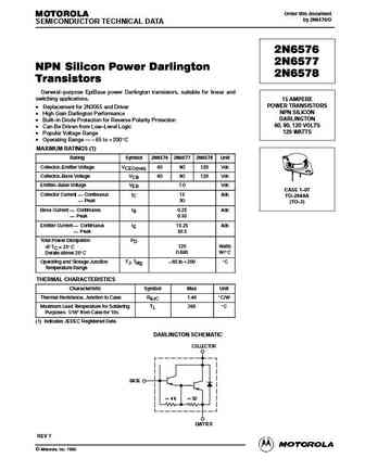
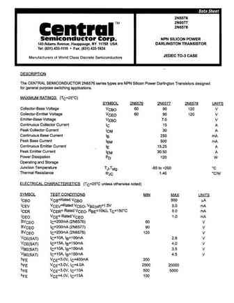
Order this document MOTOROLA by 2N6576/D SEMICONDUCTOR TECHNICAL DATA 2N6576 2N6577 NPN Silicon Power Darlington 2N6578 Transistors General purpose EpiBase power Darlington transistors, suitable for linear and switching applications. 15 AMPERE POWER TRANSISTORS Replacement for 2N3055 and Driver NPN SILICON High Gain Darlington Performance DARLINGTON Built in Dio
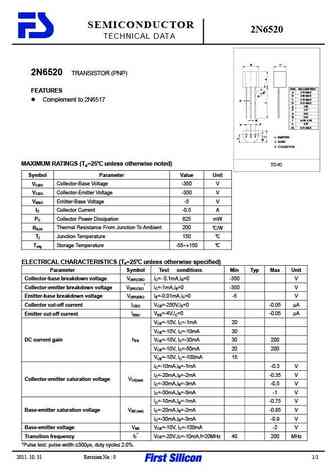
2n6515 2n6516 2n6517 2n6519 2n6520.pdf
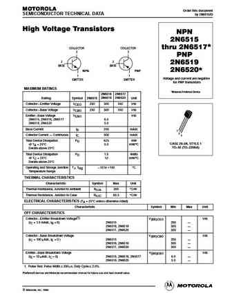
MOTOROLA Order this document SEMICONDUCTOR TECHNICAL DATA by 2N6515/D High Voltage Transistors NPN 2N6515 * COLLECTOR COLLECTOR thru 2N6517 3 3 PNP 2 2 2N6519 BASE BASE NPN PNP 2N6520 * 1 1 Voltage and current are negative EMITTER EMITTER for PNP transistors MAXIMUM RATINGS *Motorola Preferred Device 2N6516 2N6517 2N6519 2N6520 Rating Symbol 2N6515 Unit Collector Em
2n6547re.pdf
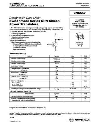
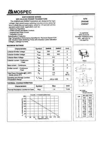
Order this document MOTOROLA by 2N6547/D SEMICONDUCTOR TECHNICAL DATA 2N6547 Designer's Data Sheet 15 AMPERE Switchmode Series NPN Silicon NPN SILICON POWER TRANSISTORS Power Transistors 300 and 400 VOLTS 175 WATTS The 2N6547 transistor is designed for high voltage, high speed, power switching in inductive circuits where fall time is critical. They are particularly suited f
2n6515 2n6517 2n6519 2n6520.pdf
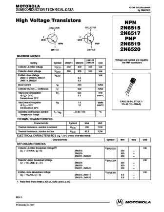
MOTOROLA Order this document SEMICONDUCTOR TECHNICAL DATA by 2N6515/D High Voltage Transistors NPN COLLECTOR COLLECTOR 2N6515 3 3 2N6517 2 2 PNP BASE BASE NPN PNP 2N6519 1 1 EMITTER EMITTER 2N6520 MAXIMUM RATINGS Voltage and current are negative 2N6517 for PNP transistors 2N6520 Rating Symbol 2N6515 2N6519 Unit Collector Emitter Voltage VCEO 250 300 350 Vdc Collector
sty112n65m5.pdf
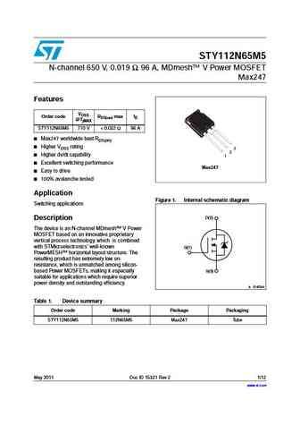
STY112N65M5 N-channel 650 V, 0.019 , 96 A, MDmesh V Power MOSFET Max247 Features VDSS Order code RDS(on) max ID @TjMAX STY112N65M5 710 V
stw62n65m5.pdf
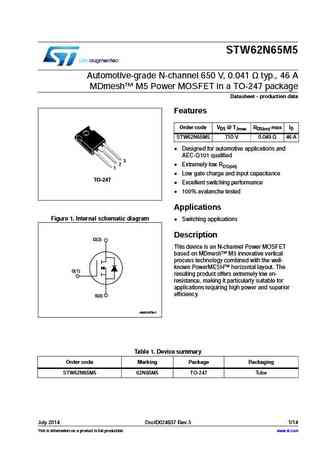
STW62N65M5 Automotive-grade N-channel 650 V, 0.041 typ., 46 A MDmesh M5 Power MOSFET in a TO-247 package Datasheet - production data Features Order code VDS @ TJmax RDS(on) max ID STW62N65M5 710 V 0.049 46 A Designed for automotive applications and AEC-Q101 qualified 3 2 Extremely low RDS(on) 1 Low gate charge and input capacitance TO-247 Excellent sw
std12n65m2.pdf
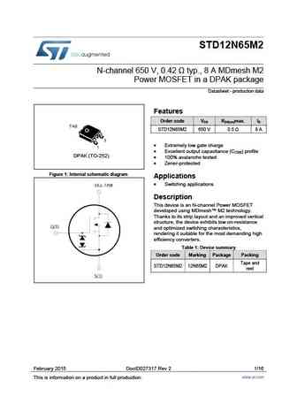
STD12N65M2 N-channel 650 V, 0.42 typ., 8 A MDmesh M2 Power MOSFET in a DPAK package Datasheet - production data Features Order code V R max. I DS DS(on) D STD12N65M2 650 V 0.5 8 A Extremely low gate charge Excellent output capacitance (COSS) profile DPAK (TO-252) 100% avalanche tested Zener-protected Figure 1 Internal schematic diagram Applicatio
stl42n65m5.pdf
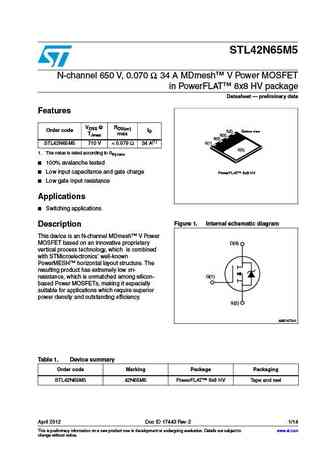
STL42N65M5 N-channel 650 V, 0.070 , 34 A MDmesh V Power MOSFET in PowerFLAT 8x8 HV package Datasheet preliminary data Features VDSS @ RDS(on) Order code ID S(2) Bottom view TJmax max S(2) S(2) G(1) STL42N65M5 710 V
2n6547 .pdf
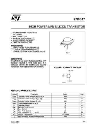
2N6547 HIGH POWER NPN SILICON TRANSISTOR STMicroelectronics PREFERRED SALESTYPE NPN TRANSISTOR HIGH VOLTAGE CAPABILITY HIGH CURRENT CAPABILITY FAST SWITCHING SPEED APPLICATIONS 1 SWITCH MODE POWER SUPPLIES 2 FLYBACK AND FORWARD SINGLE TRANSISTOR LOW POWER CONVERTERS TO-3 DESCRIPTION The 2N6547 is a silicon Multiepitaxial Mesa NPN transistor mounted in TO-3 me
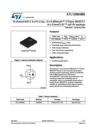
stl12n65m2.pdf
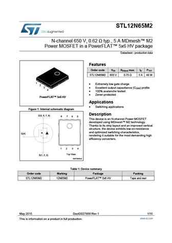
STL12N65M2 N-channel 650 V, 0.62 typ., 5 A MDmesh M2 Power MOSFET in a PowerFLAT 5x6 HV package Datasheet - production data Features Order code V R max. I P DS DS(on) D TOT STL12N65M2 650 V 0.75 5 A 48 W 1 Extremely low gate charge 2 3 Excellent output capacitance (COSS) profile 4 100% avalanche tested Zener-protected PowerFLAT 5x6 HV Ap
stb32n65m5 stf32n65m5 sti32n65m5 stp32n65m5 stw32n65m5.pdf
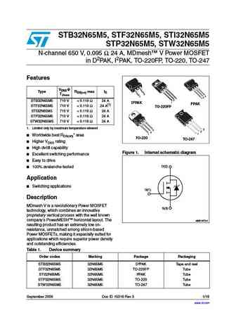
STB32N65M5, STF32N65M5, STI32N65M5 STP32N65M5, STW32N65M5 N-channel 650 V, 0.095 , 24 A, MDmesh V Power MOSFET in D2PAK, I2PAK, TO-220FP, TO-220, TO-247 Features VDSS@ Type RDS(on) max ID TJmax 3 3 1 2 3 1 2 STB32N65M5 710 V
stl22n65m5.pdf
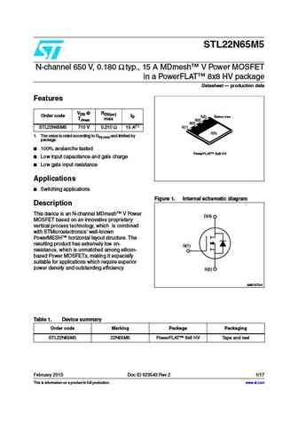
STL22N65M5 N-channel 650 V, 0.180 typ., 15 A MDmesh V Power MOSFET in a PowerFLAT 8x8 HV package Datasheet production data Features VDS @ RDS(on) Order code ID S(2) Bottom view TJmax max S(2) S(2) G(1) STL22N65M5 710 V 0.210 15 A(1) D(3) 1. The value is rated according to Rthj-case and limited by package. 100% avalanche tested PowerFLAT 8x8 HV Low
stb42n65m5 stf42n65m5 sti42n65m5 stp42n65m5 stw42n65m5.pdf
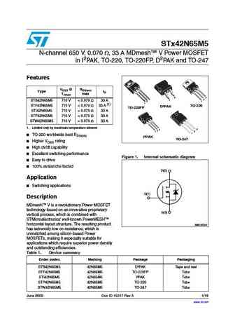
STx42N65M5 N-channel 650 V, 0.070 , 33 A MDmesh V Power MOSFET in I2PAK, TO-220, TO-220FP, D2PAK and TO-247 Features VDSS @ RDS(on) Type ID TJmax max 3 3 3 2 1 STB42N65M5 710 V
std12n65m5 stf12n65m5 sti12n65m5 stp12n65m5 stu12n65m5.pdf
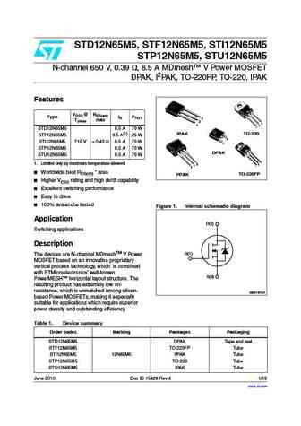
STD12N65M5, STF12N65M5, STI12N65M5 STP12N65M5, STU12N65M5 N-channel 650 V, 0.39 , 8.5 A MDmesh V Power MOSFET DPAK, I2PAK, TO-220FP, TO-220, IPAK Features VDSS @ RDS(on) Type ID PTOT 3 TJmax max 2 3 1 2 1 STD12N65M5 8.5 A 70 W IPAK TO-220 STF12N65M5 8.5 A(1) 25 W 3 STI12N65M5 710 V
2n6547.pdf

2N6547 HIGH POWER NPN SILICON TRANSISTOR STMicroelectronics PREFERRED SALESTYPE NPN TRANSISTOR HIGH VOLTAGE CAPABILITY HIGH CURRENT CAPABILITY FAST SWITCHING SPEED APPLICATIONS 1 SWITCH MODE POWER SUPPLIES 2 FLYBACK AND FORWARD SINGLE TRANSISTOR LOW POWER CONVERTERS TO-3 DESCRIPTION The 2N6547 is a silicon Multiepitaxial Mesa NPN transistor mounted in TO-3 me
stl12n65m5.pdf
STL12N65M5 N-channel 650 V, 0.475 typ., 8.5 A MDmesh V Power MOSFET in a PowerFLAT 5x6 HV package Datasheet - production data Features Order code VDSS RDS(on) max ID STL12N65M5 710 V 0.530 8.5 A Outstanding RDS(on)*area 1 Extremely large avalanche performance 2 3 Gate charge minimized 4 TM Very low intrinsic capacitance PowerFLAT 5x6 HV 100% ava
stf12n65m2.pdf
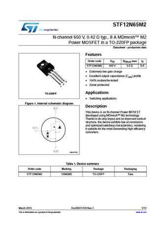
STF12N65M2 N-channel 650 V, 0.42 typ., 8 A MDmesh M2 Power MOSFET in a TO-220FP package Datasheet - production data Features Order code VDS RDS(on) max ID STF12N65M2 650 V 0.5 8 A Extremely low gate charge Excellent output capacitance (Coss) profile 100% avalanche tested 3 2 Zener-protected 1 Applications TO-220FP Switching applications Figure
2n6520.pdf
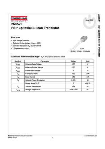
June 2009 2N6520 PNP Epitaxial Silicon Transistor Features High Voltage Transistor Collector-Emitter Voltage VCBO= -350V Collector Dissipation PC (max)=625mW Complement to 2N6517 TO-92 1 1. Emitter 2. Base 3. Collector Absolute Maximum Ratings* TA = 25 C unless otherwise noted Symbol Parameter Value Unit VCBO Collector-Base Voltage -350 V VCEO Collector-Emitte
2n6518.pdf

2N6518 High Voltage Transistor Collector-Emitter Voltage VCEO= -250V Collector Dissipation PC (max)=625mW Complement to 2N6515 TO-92 1 1. Emitter 2. Base 3. Collector PNP Epitaxial Silicon Transistor Absolute Maximum Ratings Ta=25 C unless otherwise noted Symbol Parameter Value Units VCBO Collector-Base Voltage -250 V VCEO Collector-Emitter Voltage -250 V VEBO Emitt
2n6519.pdf
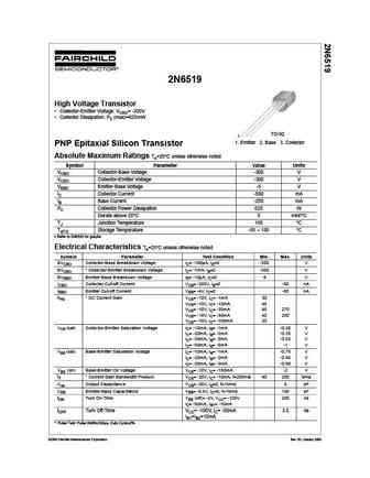
2N6519 High Voltage Transistor Collector-Emitter Voltage VCEO= -300V Collector Dissipation PC (max)=625mW TO-92 1 1. Emitter 2. Base 3. Collector PNP Epitaxial Silicon Transistor Absolute Maximum Ratings Ta=25 C unless otherwise noted Symbol Parameter Value Units VCBO Collector-Base Voltage -300 V VCEO Collector-Emitter Voltage -300 V VEBO Emitter-Base Voltage -5 V IC C
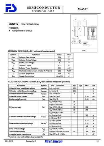
2n6517.pdf
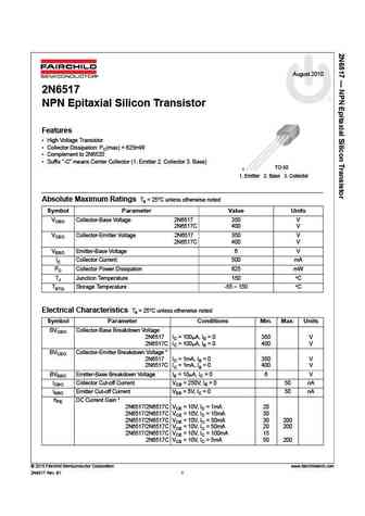
August 2010 2N6517 NPN Epitaxial Silicon Transistor Features High Voltage Transistor Collector Dissipation PC(max) = 625mW Complement to 2N6520 Suffix -C means Center Collector (1. Emitter 2. Collector 3. Base) TO-92 1 1. Emitter 2. Base 3. Collector Absolute Maximum Ratings Ta = 25 C unless otherwise noted Symbol Parameter Value Units VCBO Collector-Base Vo
2n6520.pdf
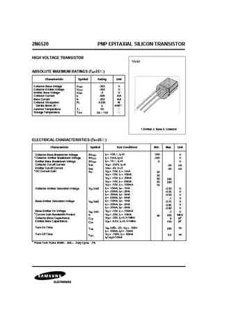
2N6520 PNP EPITAXIAL SILICON TRANSISTOR HIGH VOLTAGE TRANSISTOR TO-92 ABSOLUTE MAXIMUM RATINGS (T =25 ) A Characteristic Symbol Rating Unit Collector-Base Voltage VCBO -350 V Collector-Emitter Voltage VCEO -350 V Emitter-Base Voltage VEBO -5 V Collector Current IC -500 mA Base Current IB -250 mA Collector Dissipation PC 0.625 W Derate above 25 5 mW/ Junction Temperature TJ
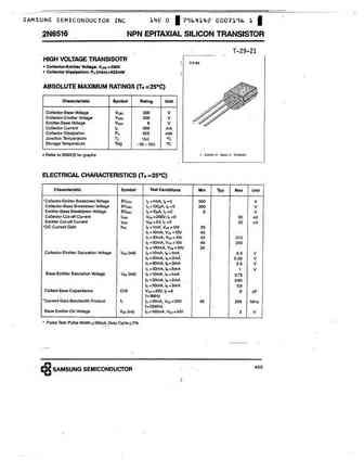
2n6515.pdf

2N6515 NPN EPITAXIAL SILICON TRANSISTOR HIGH VOLTAGE TRANSISTOR TO-92 Collector-Emitter Voltage VCEO= 250V Collector Dissipation PC (max)=625mW ABSOLUTE MAXIMUM RATINGS (T =25 ) A Characteristic Symbol Rating Unit Collector-Base Voltage VCBO 250 V Collector-Emitter Voltage VCEO 250 V Emitter-Base Voltage VEBO 6 V Collector Current IC 500 mA Collector Dissipation PC 625 mW
2n6517.pdf
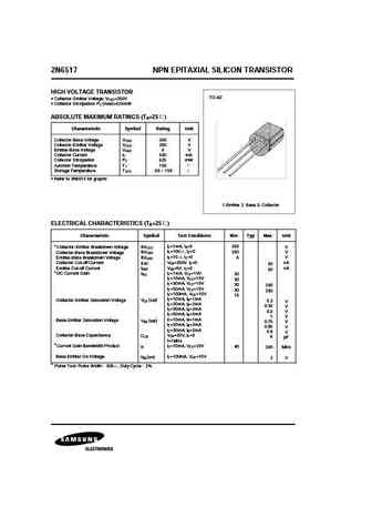
2N6517 NPN EPITAXIAL SILICON TRANSISTOR HIGH VOLTAGE TRANSISTOR TO-92 Collector-Emitter Voltage VCEO=350V Collector Dissipation PC (max)=625mW ABSOLUTE MAXIMUM RATINGS (T =25 ) A Characteristic Symbol Rating Unit Collector-Base Voltage VCBO 350 V Collector-Emitter Voltage VCEO 350 V Emitter-Base Voltage VEBO 6 V Collector Current IC 500 mA Collector Dissipation PC 625 mW
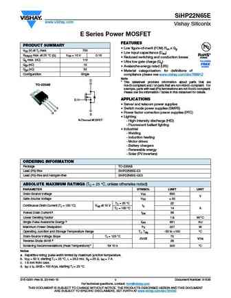
sihg22n65e.pdf
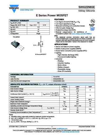
SiHG22N65E www.vishay.com Vishay Siliconix E Series Power MOSFET FEATURES PRODUCT SUMMARY Low figure-of-merit (FOM) Ron x Qg VDS (V) at TJ max. 700 Low input capacitance (Ciss) RDS(on) max. at 25 C ( ) VGS = 10 V 0.18 Reduced switching and conduction losses Available Qg max. (nC) 110 Ultra low gate charge (Qg) Qgs (nC) 15 Avalanche energy rated (UIS) Availab
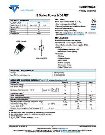
sihp12n65e.pdf
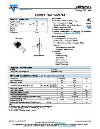
SiHP12N65E www.vishay.com Vishay Siliconix E Series Power MOSFET FEATURES PRODUCT SUMMARY Low figure-of-merit (FOM) Ron x Qg VDS (V) at TJ max. 700 Low input capacitance (Ciss) RDS(on) max. at 25 C ( ) VGS = 10 V 0.38 Reduced switching and conduction losses Qg max. (nC) 70 Ultra low gate charge (Qg) Qgs (nC) 9 Avalanche energy rated (UIS) Qgd (nC) 16 M
sihf12n65e.pdf
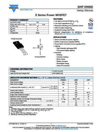
SiHF12N65E www.vishay.com Vishay Siliconix E Series Power MOSFET FEATURES PRODUCT SUMMARY Low figure-of-merit (FOM) Ron x Qg VDS (V) at TJ max. 700 Low input capacitance (Ciss) RDS(on) max. at 25 C ( ) VGS = 10 V 0.38 Reduced switching and conduction losses Qg max. (nC) 70 Ultra low gate charge (Qg) Qgs (nC) 9 Avalanche energy rated (UIS) Qgd (nC) 16 M
sihb22n65e.pdf
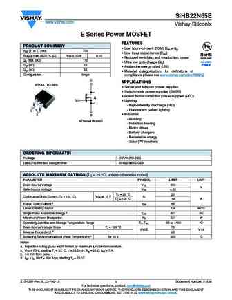
SiHB22N65E www.vishay.com Vishay Siliconix E Series Power MOSFET FEATURES PRODUCT SUMMARY Low figure-of-merit (FOM) Ron x Qg VDS (V) at TJ max. 700 Low input capacitance (Ciss) RDS(on) max. at 25 C ( ) VGS = 10 V 0.18 Reduced switching and conduction losses Qg max. (nC) 110 Ultra low gate charge (Qg) Qgs (nC) 15 Avalanche energy rated (UIS) Qgd (nC) 32
sihf22n65e.pdf
SiHF22N65E www.vishay.com Vishay Siliconix E Series Power MOSFET FEATURES PRODUCT SUMMARY Low figure-of-merit (FOM) Ron x Qg VDS (V) at TJ max. 700 Low input capacitance (Ciss) RDS(on) max. at 25 C ( ) VGS = 10 V 0.18 Reduced switching and conduction losses Available Qg max. (nC) 110 Ultra low gate charge (Qg) Qgs (nC) 15 Avalanche energy rated (UIS) Availa
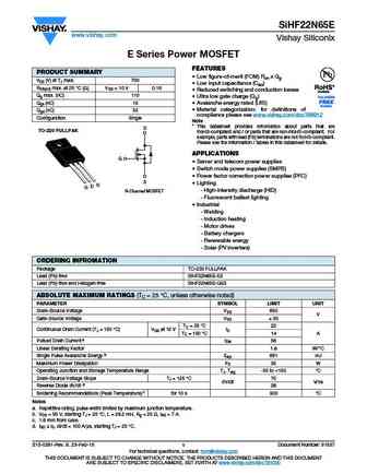
sihp22n65e.pdf
SiHP22N65E www.vishay.com Vishay Siliconix E Series Power MOSFET FEATURES PRODUCT SUMMARY Low figure-of-merit (FOM) Ron x Qg VDS (V) at TJ max. 700 Low input capacitance (Ciss) RDS(on) max. at 25 C ( ) VGS = 10 V 0.18 Reduced switching and conduction losses Available Qg max. (nC) 110 Ultra low gate charge (Qg) Qgs (nC) 15 Avalanche energy rated (UIS) Availab
sihb12n65e.pdf
SiHB12N65E www.vishay.com Vishay Siliconix E Series Power MOSFET FEATURES PRODUCT SUMMARY Low figure-of-merit (FOM) Ron x Qg VDS (V) at TJ max. 700 Low input capacitance (Ciss) RDS(on) max. at 25 C ( ) VGS = 10 V 0.38 Reduced switching and conduction losses Qg max. (nC) 70 Ultra low gate charge (Qg) Qgs (nC) 9 Avalanche energy rated (UIS) Qgd (nC) 16 M
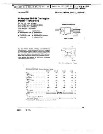
2n6551 2n6552 2n6553 2n6554 2n6555 2n6556.pdf
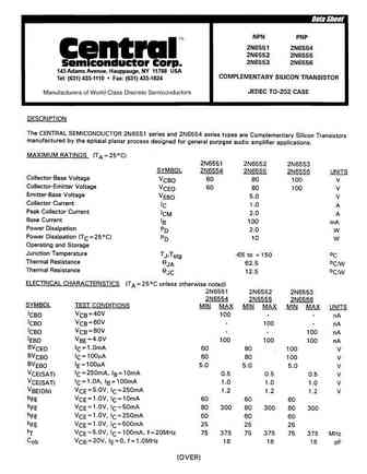
145 Adams Avenue, Hauppauge, NY 11788 USA Tel (631) 435-1110 Fax (631) 435-1824
2n6544 2n6545.pdf
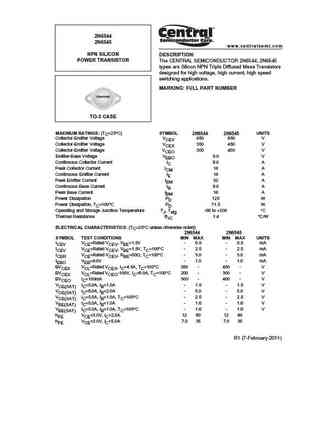
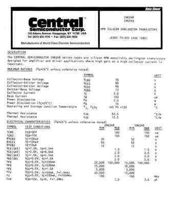
2N6544 2N6545 www.centralsemi.com NPN SILICON DESCRIPTION POWER TRANSISTOR The CENTRAL SEMICONDUCTOR 2N6544, 2N6545 types are Silicon NPN Triple Diffused Mesa Transistors designed for high voltage, high current, high speed switching applications. MARKING FULL PART NUMBER TO-3 CASE MAXIMUM RATINGS (TC=25 C) SYMBOL 2N6544 2N6545 UNITS Collector-Emitter Voltage VCEV 650 850 V
2n6576 2n6577 2n6578.pdf
145 Adams Avenue, Hauppauge, NY 11788 USA Tel (631) 435-1110 Fax (631) 435-1824
2n6548 2n6549.pdf
145 Adams Avenue, Hauppauge, NY 11788 USA Tel (631) 435-1110 Fax (631) 435-1824
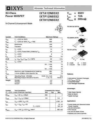
ixta12n65x2 ixth12n65x2 ixtp12n65x2.pdf
Advance Technical Information X2-Class VDSS = 650V IXTA12N65X2 Power MOSFET ID25 = 12A IXTP12N65X2 RDS(on) 300m IXTH12N65X2 N-Channel Enhancement Mode TO-263 AA (IXTA) G S D (Tab) Symbol Test Conditions Maximum Ratings TO-220AB (IXTP) VDSS TJ = 25 C to 150 C 650 V VDGR TJ = 25 C to 150 C, RGS = 1M 650 V VGSS Continuous 30
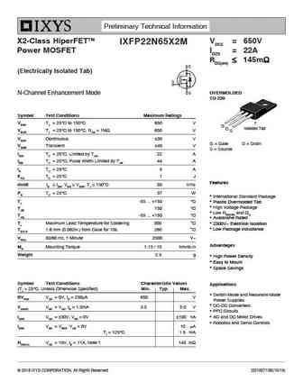
ixfp22n65x2m.pdf
Preliminary Technical Information X2-Class HiperFETTM VDSS = 650V IXFP22N65X2M Power MOSFET ID25 = 22A RDS(on) 145m (Electrically Isolated Tab) OVERMOLDED N-Channel Enhancement Mode TO-220 Symbol Test Conditions Maximum Ratings VDSS TJ = 25 C to 150 C 650 V G Isolated Tab D VDGR TJ = 25 C to 150 C, RGS = 1M 650 V S VGSS Conti
ixfp12n65x2m ixfp12n65x2 ixfa12n65x2 ixfh12n65x2.pdf
X2-Class HiPERFET VDSS = 650V IXFA12N65X2 Power MOSFET ID25 = 12A IXFP12N65X2 RDS(on) 310m IXFH12N65X2 N-Channel Enhancement Mode Avalanche Rated TO-263 (IXFA) G S D (Tab) Symbol Test Conditions Maximum Ratings TO-220 (IXFP) VDSS TJ = 25 C to 150 C 650 V VDGR TJ = 25 C to 150 C, RGS = 1M 650 V VGSS Continuous 30 V VGSM Tr
ixth62n65x2.pdf
Advance Technical Information X2-Class VDSS = 650V IXTH62N65X2 Power MOSFET ID25 = 62A RDS(on) 52m N-Channel Enhancement Mode Avalanche Rated TO-247 G D Symbol Test Conditions Maximum Ratings S D (Tab) VDSS TJ = 25 C to 150 C 650 V G = Gate D = Drain VDGR TJ = 25 C to 150 C, RGS = 1M 650 V S = Source Tab = Drain VGSS Continu
ixtr102n65x2.pdf
Advance Technical Information X2-Class VDSS = 650V IXTR102N65X2 Power MOSFET ID25 = 54A RDS(on) 33m (Electrically Isolated Tab) N-Channel Enhancement Mode Avalanche Rated ISOPLUS247 E153432 Symbol Test Conditions Maximum Ratings VDSS TJ = 25 C to 150 C 650 V VDGR TJ = 25 C to 150 C, RGS = 1M 650 V VGSS Continuous 30 V G VG
ixtn102n65x2.pdf
Advance Technical Information X2-Class VDSS = 650V IXTN102N65X2 Power MOSFET ID25 = 76A RDS(on) 30m N-Channel Enhancement Mode Avalanche Rated miniBLOC Fast Intrinsic Diode E153432 S G Symbol Test Conditions Maximum Ratings VDSS TJ = 25 C to 150 C 650 V VDGR TJ = 25 C to 150 C, RGS = 1M 650 V S VGSS Continuous 30 V D VG
ixtp32n65xm.pdf
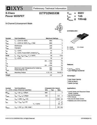
Preliminary Technical Information X-Class VDSS = 650V IXTP32N65XM Power MOSFET ID25 = 14A RDS(on) 135m N-Channel Enhancement Mode OVERMOLDED Symbol Test Conditions Maximum Ratings VDSS TJ = 25 C to 150 C 650 V G D VDGR TJ = 25 C to 150 C, RGS = 1M 650 V S VGSS Continuous 30 V G = Gate D = Drain VGSM Transient 40 V S = S
ixth32n65x ixtp32n65x ixtq32n65x.pdf
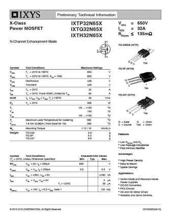
Preliminary Technical Information X-Class VDSS = 650V IXTP32N65X Power MOSFET ID25 = 32A IXTQ32N65X RDS(on) 135m IXTH32N65X N-Channel Enhancement Mode TO-220AB (IXTP) G D Tab S Symbol Test Conditions Maximum Ratings TO-3P (IXTQ) VDSS TJ = 25 C to 150 C 650 V VDGR TJ = 25 C to 150 C, RGS = 1M 650 V G VGSS Continuous 30 V
ixfa22n65x2 ixfp22n65x2 ixfh22n65x2.pdf
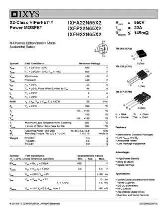
X2-Class HiPerFETTM VDSS = 650V IXFA22N65X2 Power MOSFET ID25 = 22A IXFP22N65X2 RDS(on) 145m IXFH22N65X2 N-Channel Enhancement Mode Avalanche Rated TO-263 (IXFA) G S Symbol Test Conditions Maximum Ratings D (Tab) TO-220 (IXFP) VDSS TJ = 25 C to 150 C 650 V VDGR TJ = 25 C to 150 C, RGS = 1M 650 V VGSS Continuous 30 V VGSM T
ixth52n65x.pdf
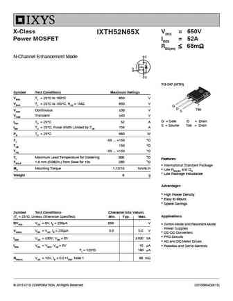
X-Class VDSS = 650V IXTH52N65X Power MOSFET ID25 = 52A RDS(on) 68m N-Channel Enhancement Mode TO-247 (IXTH) Symbol Test Conditions Maximum Ratings VDSS TJ = 25 C to 150 C 650 V VDGR TJ = 25 C to 150 C, RGS = 1M 650 V G D Tab VGSS Continuous 30 V S VGSM Transient 40 V G = Gate D = Drain ID25 TC = 25 C52 A S = Source
ixtk102n65x2 ixtx102n65x2.pdf
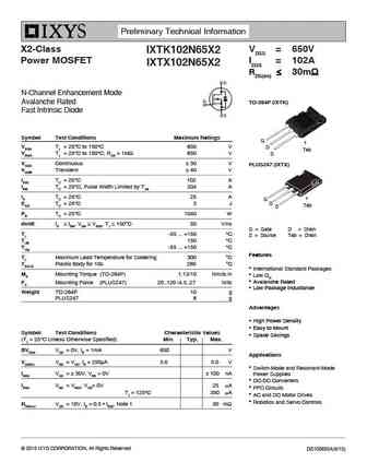
Preliminary Technical Information X2-Class VDSS = 650V IXTK102N65X2 Power MOSFET ID25 = 102A IXTX102N65X2 RDS(on) 30m N-Channel Enhancement Mode Avalanche Rated TO-264P (IXTK) Fast Intrinsic Diode Symbol Test Conditions Maximum Ratings G VDSS TJ = 25 C to 150 C 650 V D Tab VDGR TJ = 25 C to 150 C, RGS = 1M 650 V S VGSS Contin
ixfa22n65x2 ixfh22n65x2 ixfp22n65x2.pdf
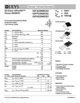
Advance Technical Information X2-Class HiPerFETTM VDSS = 650V IXFA22N65X2 Power MOSFET ID25 = 22A IXFP22N65X2 RDS(on) 160m IXFH22N65X2 N-Channel Enhancement Mode TO-263 AA (IXFA) Avalanche Rated Fast Intrinsic Diode G S D (Tab) Symbol Test Conditions Maximum Ratings TO-220AB (IXFP) VDSS TJ = 25 C to 150 C 650 V VDGR TJ = 25 C to
ixtp2n65x2 ixty2n65x2.pdf
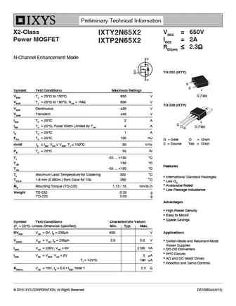
Preliminary Technical Information X2-Class VDSS = 650V IXTY2N65X2 Power MOSFET ID25 = 2A IXTP2N65X2 RDS(on) 2.3 N-Channel Enhancement Mode TO-252 (IXTY) G S Symbol Test Conditions Maximum Ratings D (Tab) VDSS TJ = 25 C to 150 C 650 V VDGR TJ = 25 C to 150 C, RGS = 1M 650 V TO-220 (IXTP) VGSS Continuous 30 V VGSM Transient
nvhl072n65s3.pdf
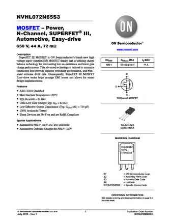
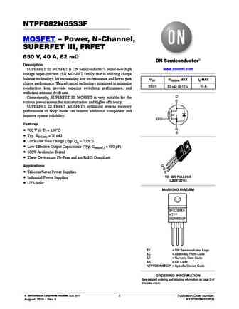
NVHL072N65S3 MOSFET Power, N-Channel, SUPERFET) III, Automotive, Easy-drive 650 V, 44 A, 72 mW www.onsemi.com Description SuperFET III MOSFET is ON Semiconductor s brand-new high BVDSS RDS(on) MAX ID MAX voltage super-junction (SJ) MOSFET family that is utilizing charge balance technology for outstanding low on-resistance and lower gate 650 V 72 m @ 10 V 44 A charge performa
nvb082n65s3f.pdf
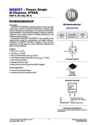
MOSFET - Power, Single N-Channel, D2PAK 650 V, 82 mW, 40 A NVB082N65S3F Description SUPERFET III MOSFET is ON Semiconductor s brand-new high www.onsemi.com voltage super-junction (SJ) MOSFET family that is utilizing charge balance technology for outstanding low on-resistance and lower gate charge performance. This advanced technology is tailored to minimize V(BR)DSS RDS(ON) MAX ID
ntp082n65s3f.pdf
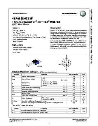
www.onsemi.com NTP082N65S3F N-Channel SuperFET III FRFET MOSFET 650 V, 40 A, 82 m Features Description 700 V @ TJ = 150 oC SuperFET III MOSFET is ON Semiconductor s brand-new high voltage super-junction (SJ) MOSFET family that is utilizing Typ. RDS(on) = 70 m charge balance technology for outstanding low on-resistance Ultra Low Gate Charge (Typ. Qg = 81 nC)
nvhl082n65s3f.pdf
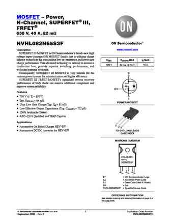
MOSFET Power, N-Channel, SUPERFET) III, FRFET) 650 V, 40 A, 82 mW NVHL082N65S3F www.onsemi.com Description SUPERFET III MOSFET is ON Semiconductor s brand-new high voltage super-junction (SJ) MOSFET family that is utilizing charge balance technology for outstanding low on-resistance and lower gate VDSS RDS(ON) MAX ID MAX charge performance. This advanced technology is tailored
nthl082n65s3f.pdf
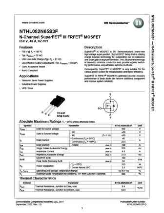
www.onsemi.com NTHL082N65S3F N-Channel SuperFET III FRFET MOSFET 650 V, 40 A, 82 m Features Description 700 V @ TJ = 150 oC SuperFET III MOSFET is ON Semiconductor s brand-new high voltage super-junction (SJ) MOSFET family that is utilizing Typ. RDS(on) = 70 m charge balance technology for outstanding low on-resistance Ultra Low Gate Charge (Typ. Qg = 81 nC)
2n6515 2n6517 2n6520.pdf
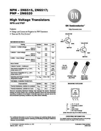
NPN - 2N6515, 2N6517; PNP - 2N6520 High Voltage Transistors NPN and PNP Features http //onsemi.com Voltage and Current are Negative for PNP Transistors COLLECTOR These are Pb-Free Devices* 3 2 BASE MAXIMUM RATINGS COLLECTOR NPN Rating Symbol Value Unit 3 1 Collector - Emitter Voltage VCEO Vdc EMITTER 2N6515 250 2 2N6517, 2N6520 350 BASE Collector - Base Voltage V
2n6517bu 2n6517ta 2n6517cta.pdf

NPN Epitaxial Silicon Transistor 2N6517 Features High Voltage Transistor www.onsemi.com Collector Dissipation PC(max) = 625 mW Complement to 2N6520 Suffix -C means Center Collector (1. Emitter 2. Collector 3. Base) ABSOLUTE MAXIMUM RATINGS (Values are at TA = 25 C unless otherwise noted.) Symbol Parameter Value Unit VCBO Collector-Base Voltage V 1 1 2 2
ntb082n65s3f.pdf
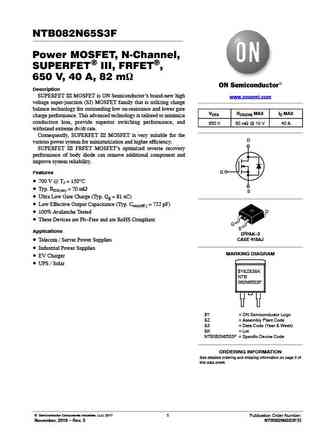
NTB082N65S3F Power MOSFET, N Channel, SUPERFET) III, FRFET), 650 V, 40 A, 82 mW Description SUPERFET III MOSFET is ON Semiconductor s brand-new high www.onsemi.com voltage super-junction (SJ) MOSFET family that is utilizing charge balance technology for outstanding low on-resistance and lower gate VDSS RDS(ON) MAX ID MAX charge performance. This advanced technology is tailored to
2n6517.pdf
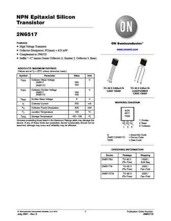
NPN Epitaxial Silicon Transistor 2N6517 Features High Voltage Transistor www.onsemi.com Collector Dissipation PC(max) = 625 mW Complement to 2N6520 Suffix -C means Center Collector (1. Emitter 2. Collector 3. Base) ABSOLUTE MAXIMUM RATINGS (Values are at TA = 25 C unless otherwise noted.) Symbol Parameter Value Unit VCBO Collector-Base Voltage V 1 1 2 2
nvb072n65s3.pdf
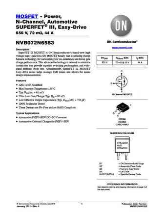
MOSFET - Power, N-Channel, Automotive SUPERFET) III, Easy-Drive 650 V, 72 mW, 44 A NVB072N65S3 www.onsemi.com Description SuperFET III MOSFET is ON Semiconductor s brand-new high voltage super-junction (SJ) MOSFET family that is utilizing charge BVDSS RDS(on) MAX ID MAX balance technology for outstanding low on-resistance and lower gate charge performance. This advanced technology
ntpf082n65s3f.pdf
NTPF082N65S3F MOSFET Power, N-Channel, SUPERFET III, FRFET 650 V, 40 A, 82 mW Description www.onsemi.com SUPERFET III MOSFET is ON Semiconductor s brand-new high voltage super-junction (SJ) MOSFET family that is utilizing charge balance technology for outstanding low on-resistance and lower gate VDS RDS(ON) MAX ID MAX charge performance. This advanced technology is tailored to m
2n65l-aa3-r 2n65g-aa3-r 2n65l-ta3-t 2n65g-ta3-t 2n65l-tf3-t 2n65g-tf3-t 2n65l-tf1-t 2n65g-tf1-t 2n65l-tf2-t 2n65g-tf2-t 2n65l-tn3-r 2n65g-tn3-r.pdf

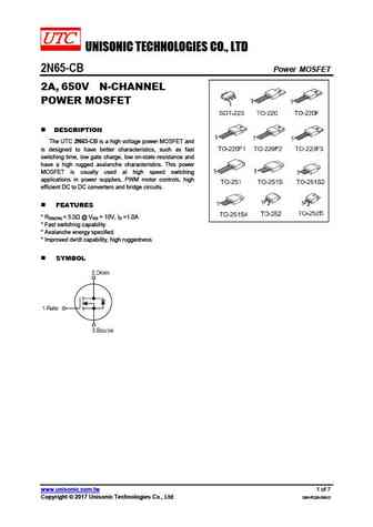
UNISONIC TECHNOLOGIES CO., LTD 2N65-CB Power MOSFET 2A, 650V N-CHANNEL POWER MOSFET DESCRIPTION The UTC 2N65-CB is a high voltage power MOSFET and is designed to have better characteristics, such as fast switching time, low gate charge, low on-state resistance and have a high rugged avalanche characteristics. This power MOSFET is usually used at high speed switching appli
2n65l.pdf
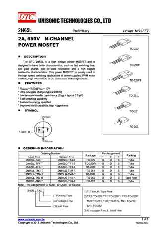
UNISONIC TECHNOLOGIES CO., LTD 2N65L Preliminary Power MOSFET 2A, 650V N-CHANNEL POWER MOSFET 1 TO-220 DESCRIPTION The UTC 2N65L is a high voltage power MOSFET and is 1 TO-220F designed to have better characteristics, such as fast switching time, low gate charge, low on-state resistance and a high rugged avalanche characteristics. This power MOSFET is usually used in the
2n65l-tms4-t 2n65g-tms4-t 2n65l-tn3-r 2n65g-tn3-r 2n65l-tnd-r 2n65g-tnd-r 2n65g-k08-5060-r.pdf

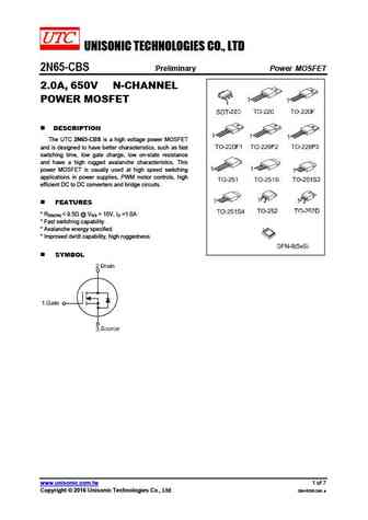
UNISONIC TECHNOLOGIES CO., LTD 2N65-CBS Preliminary Power MOSFET 2.0A, 650V N-CHANNEL POWER MOSFET DESCRIPTION The UTC 2N65-CBS is a high voltage power MOSFET and is designed to have better characteristics, such as fast switching time, low gate charge, low on-state resistance and have a high rugged avalanche characteristics. This power MOSFET is usually used at high speed s
22n65.pdf
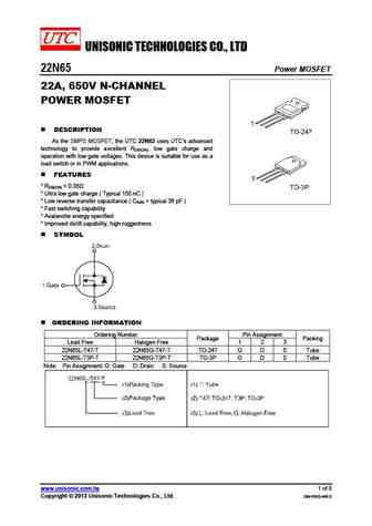
UNISONIC TECHNOLOGIES CO., LTD 22N65 Power MOSFET 22A, 650V N-CHANNEL POWER MOSFET DESCRIPTION As the SMPS MOSFET, the UTC 22N65 uses UTC s advanced technology to provide excellent RDS(ON), low gate charge and operation with low gate voltages. This device is suitable for use as a load switch or in PWM applications. FEATURES * RDS(ON)
2n65kl-tm3-t 2n65kg-tm3-t 2n65kl-tms-t 2n65kg-tms-t 2n65kl-tms2-t 2n65kg-tms2-t 2n65kl-tms4-t 2n65kg-tms4-t 2n65kl-tn3-r 2n65kg-tn3-r 2n65kl-tnd-r.pdf
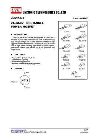
UNISONIC TECHNOLOGIES CO., LTD 2N65K-MT Power MOSFET 2A, 650V N-CHANNEL POWER MOSFET DESCRIPTION The UTC 2N65K-MT is a high voltage power MOSFET and is designed to have better characteristics, such as fast switching time, low gate charge, low on-state resistance and have a high rugged avalanche characteristics. This power MOSFET is usually used at high speed switching appl
2n65g-aa3-r 2n65l-ta3-t 2n65g-ta3-t 2n65l-tf3-t 2n65g-tf3-t 2n65l-tf1-t 2n65g-tf1-t 2n65l-tf2-t 2n65g-tf2-t.pdf

UNISONIC TECHNOLOGIES CO., LTD 2N65-CBS Preliminary Power MOSFET 2.0A, 650V N-CHANNEL POWER MOSFET DESCRIPTION The UTC 2N65-CBS is a high voltage power MOSFET and is designed to have better characteristics, such as fast switching time, low gate charge, low on-state resistance and have a high rugged avalanche characteristics. This power MOSFET is usually used at high speed s
2n65l-tf3t-t 2n65g-tf3t-t 2n65l-tm3-t 2n65g-tm3-t 2n65l-tms-t 2n65g-tms-t 2n65l-tms2-t 2n65g-tms2-t.pdf
UNISONIC TECHNOLOGIES CO., LTD 2N65-CBS Preliminary Power MOSFET 2.0A, 650V N-CHANNEL POWER MOSFET DESCRIPTION The UTC 2N65-CBS is a high voltage power MOSFET and is designed to have better characteristics, such as fast switching time, low gate charge, low on-state resistance and have a high rugged avalanche characteristics. This power MOSFET is usually used at high speed s
2n65kl-ta3-t 2n65kg-ta3-t 2n65kl-tf3-t 2n65kg-tf3-t 2n65kl-tf1-t 2n65kg-tf1-t 2n65kl-tf2-t 2n65kg-tf2-t 2n65kl-tf3t-t 2n65kg-tf3t-t 2n65kg-tnd-r.pdf

UNISONIC TECHNOLOGIES CO., LTD 2N65K-MT Power MOSFET 2A, 650V N-CHANNEL POWER MOSFET DESCRIPTION The UTC 2N65K-MT is a high voltage power MOSFET and is designed to have better characteristics, such as fast switching time, low gate charge, low on-state resistance and have a high rugged avalanche characteristics. This power MOSFET is usually used at high speed switching appl
2n65z.pdf
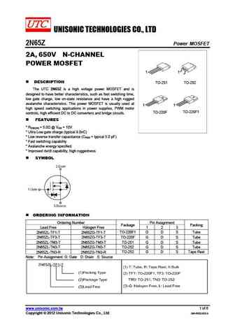
UNISONIC TECHNOLOGIES CO., LTD 2N65Z Power MOSFET 2A, 650V N-CHANNEL POWER MOSFET 1 1 DESCRIPTION TO-251 TO-252 The UTC 2N65Z is a high voltage power MOSFET and is designed to have better characteristics, such as fast switching time, low gate charge, low on-state resistance and have a high rugged avalanche characteristics. This power MOSFET is usually used at 1 1 high sp
12n65kl-ta3-t 12n65kg-ta3-t 12n65kl-tf1-t 12n65kg-tf1-t 12n65kl-tf2-t 12n65kg-tf2-t 12n65kl-tf3-t 12n65kg-tf3-t 12n65kl-tq2-t 12n65kg-tq2-t 12n65kl-tq2-r 12n65kg-tq2-r.pdf
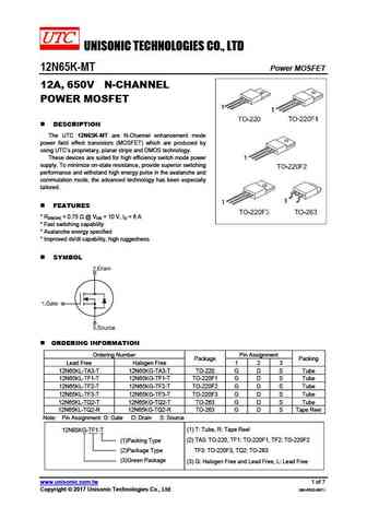
UNISONIC TECHNOLOGIES CO., LTD 12N65K-MT Power MOSFET 12A, 650V N-CHANNEL POWER MOSFET DESCRIPTION The UTC 12N65K-MT are N-Channel enhancement mode power field effect transistors (MOSFET) which are produced by using UTC s proprietary, planar stripe and DMOS technology. These devices are suited for high efficiency switch mode power supply. To minimize on-state resistance,
2n65l-ta3-t 2n65g-ta3-t 2n65l-tf1-t 2n65g-tf1-t 2n65l-tf2-t 2n65g-tf2-t 2n65l-tf3-t 2n65g-tf3-t 2n65l-tf3t-t 2n65g-tf3t-t 2n65l-tm3-t 2n65g-tm3-t 2n65g-t6c-k.pdf

UNISONIC TECHNOLOGIES CO., LTD 2N65 Power MOSFET 2A, 650V N-CHANNEL POWER MOSFET DESCRIPTION The UTC 2N65 is a high voltage power MOSFET and is designed to have better characteristics, such as fast switching time, low gate charge, low on-state resistance and have a high rugged avalanche characteristics. This power MOSFET is usually used at high speed switching applications
2n65k.pdf
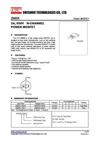
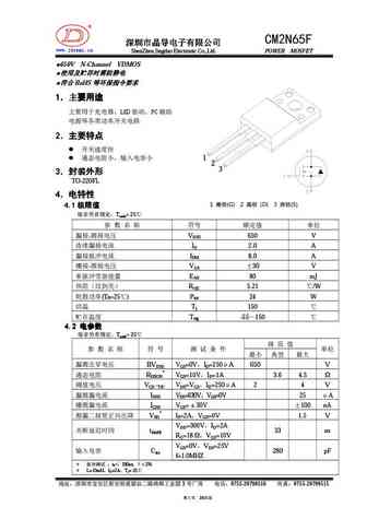
UNISONIC TECHNOLOGIES CO., LTD 2N65K Power MOSFET 2A, 650V N-CHANNEL POWER MOSFET DESCRIPTION The UTC 2N65K is a high voltage power MOSFET and is designed to have better characteristics, such as fast switching time, low gate charge, low on-state resistance and have a high rugged avalanche characteristics. This power MOSFET is usually used at high speed switching applicatio
2n65l-tma-t 2n65g-tma-t 2n65l-tms-t 2n65g-tms-t 2n65l-tn3-r 2n65g-tn3-r 2n65l-tn3-t 2n65g-tn3-t 2n65l-t2q-t 2n65g-t2q-t 2n65l-t60-k 2n65g-t60-k 2n65l-t6c-k.pdf
UNISONIC TECHNOLOGIES CO., LTD 2N65 Power MOSFET 2A, 650V N-CHANNEL POWER MOSFET DESCRIPTION The UTC 2N65 is a high voltage power MOSFET and is designed to have better characteristics, such as fast switching time, low gate charge, low on-state resistance and have a high rugged avalanche characteristics. This power MOSFET is usually used at high speed switching applications
2n65l-tf3t-t 2n65g-tf3t-t 2n65l-tm3-t 2n65g-tm3-t 2n65l-tms-t 2n65g-tms-t 2n65l-tms2-t 2n65g-tms2-t 2n65l-tms4-t 2n65g-tms4-t 2n65l-tnd-r 2n65g-tnd-r.pdf
UNISONIC TECHNOLOGIES CO., LTD 2N65-CB Power MOSFET 2A, 650V N-CHANNEL POWER MOSFET DESCRIPTION The UTC 2N65-CB is a high voltage power MOSFET and is designed to have better characteristics, such as fast switching time, low gate charge, low on-state resistance and have a high rugged avalanche characteristics. This power MOSFET is usually used at high speed switching appli

2n6546-t1-t3 2n6547-t1-t3.pdf
The documentation and process conversion measures necessary to comply with this document shall be INCH-POUND completed by 13 February 2014. MIL-PRF-19500/525F 13 December 2013 SUPERSEDING MIL-PRF-19500/525E 1 October 2009 PERFORMANCE SPECIFICATION SHEET SEMICONDUCTOR DEVICE, TRANSISTOR, NPN, SILICON, POWER TYPES 2N6546, 2N6546T1, 2N6546T3, 2N6547, 2N6547T1, AND 2N6547
2n6511.pdf

2N6511 Dimensions in mm (inches). Bipolar NPN Device in a Hermetically sealed TO3 25.15 (0.99) 6.35 (0.25) 26.67 (1.05) 9.15 (0.36) Metal Package. 10.67 (0.42) 11.18 (0.44) 1.52 (0.06) 3.43 (0.135) 1 2 Bipolar NPN Device. 3 VCEO = 250V (case) 3.84 (0.151) 4.09 (0.161) 7.92 (0.312) IC = 7A 12.70 (0.50) All Semelab hermetically sealed products can be processed in a
2n6560.pdf

2N6560 Dimensions in mm (inches). Bipolar NPN Device in a Hermetically sealed TO3 25.15 (0.99) 6.35 (0.25) 26.67 (1.05) 9.15 (0.36) Metal Package. 10.67 (0.42) 11.18 (0.44) 1.52 (0.06) 3.43 (0.135) 1 2 Bipolar NPN Device. 3 VCEO = 450V (case) 3.84 (0.151) 4.09 (0.161) 7.92 (0.312) IC = 10A 12.70 (0.50) All Semelab hermetically sealed products can be processed in
2n6583.pdf

2N6583 Dimensions in mm (inches). Bipolar NPN Device in a Hermetically sealed TO3 25.15 (0.99) 6.35 (0.25) 26.67 (1.05) 9.15 (0.36) Metal Package. 10.67 (0.42) 11.18 (0.44) 1.52 (0.06) 3.43 (0.135) 1 2 Bipolar NPN Device. 3 VCEO = 400V (case) 3.84 (0.151) 4.09 (0.161) 7.92 (0.312) IC = 10A 12.70 (0.50) All Semelab hermetically sealed products can be processed in
2n6512.pdf
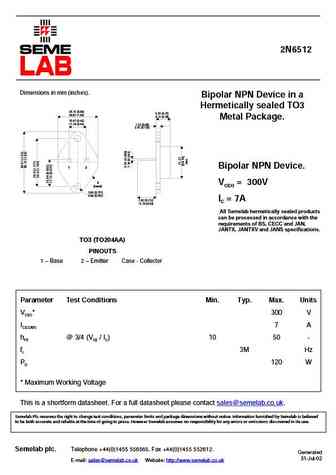
2N6512 Dimensions in mm (inches). Bipolar NPN Device in a Hermetically sealed TO3 25.15 (0.99) 6.35 (0.25) 26.67 (1.05) 9.15 (0.36) Metal Package. 10.67 (0.42) 11.18 (0.44) 1.52 (0.06) 3.43 (0.135) 1 2 Bipolar NPN Device. 3 VCEO = 300V (case) 3.84 (0.151) 4.09 (0.161) 7.92 (0.312) IC = 7A 12.70 (0.50) All Semelab hermetically sealed products can be processed in a
2n6561.pdf
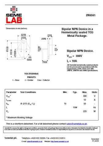
2N6561 Dimensions in mm (inches). Bipolar NPN Device in a Hermetically sealed TO3 25.15 (0.99) 6.35 (0.25) 26.67 (1.05) 9.15 (0.36) Metal Package. 10.67 (0.42) 11.18 (0.44) 1.52 (0.06) 3.43 (0.135) 1 2 Bipolar NPN Device. 3 VCEO = 300V (case) 3.84 (0.151) 4.09 (0.161) 7.92 (0.312) IC = 10A 12.70 (0.50) All Semelab hermetically sealed products can be processed in
2n6581.pdf

2N6581 Dimensions in mm (inches). Bipolar NPN Device in a Hermetically sealed TO3 25.15 (0.99) 6.35 (0.25) 26.67 (1.05) 9.15 (0.36) Metal Package. 10.67 (0.42) 11.18 (0.44) 1.52 (0.06) 3.43 (0.135) 1 2 Bipolar NPN Device. 3 VCEO = 450V (case) 3.84 (0.151) 4.09 (0.161) 7.92 (0.312) IC = 10A 12.70 (0.50) All Semelab hermetically sealed products can be processed in
2n6575.pdf

2N6575 Dimensions in mm (inches). Bipolar NPN Device in a Hermetically sealed TO3 25.15 (0.99) 6.35 (0.25) 26.67 (1.05) 9.15 (0.36) Metal Package. 10.67 (0.42) 11.18 (0.44) 1.52 (0.06) 3.43 (0.135) 1 2 Bipolar NPN Device. 3 VCEO = 300V (case) 3.84 (0.151) 4.09 (0.161) 7.92 (0.312) IC = 10A 12.70 (0.50) All Semelab hermetically sealed products can be processed in
2n6535.pdf

2N6535 Dimensions in mm (inches). Bipolar NPN Device in a Hermetically sealed TO66 6.35 (0.250) Metal Package. 8.64 (0.340) 3.68 (0.145) rad. 3.61 (0.142) max. 4.08(0.161) rad. Bipolar NPN Device. 1 2 VCEO = 100V IC = 8A All Semelab hermetically sealed products can be processed in accordance with the requirements of BS, CECC and JAN, JANTX, JANTXV and JANS speci
2n6537.pdf
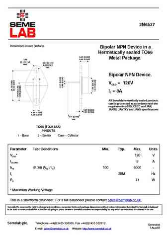
2N6537 Dimensions in mm (inches). Bipolar NPN Device in a Hermetically sealed TO66 6.35 (0.250) Metal Package. 8.64 (0.340) 3.68 (0.145) rad. 3.61 (0.142) max. 4.08(0.161) rad. Bipolar NPN Device. 1 2 VCEO = 120V IC = 8A All Semelab hermetically sealed products can be processed in accordance with the requirements of BS, CECC and JAN, JANTX, JANTXV and JANS speci
2n6520.pdf
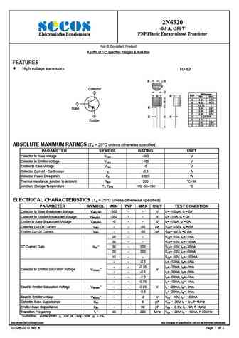
2N6520 -0.5 A, -350 V PNP Plastic Encapsulated Transistor Elektronische Bauelemente RoHS Compliant Product A suffix of -C specifies halogen & lead-free FEATURES High voltage transistors TO-92 G H Collector J Millimeter REF. A D Min. Max. A 4.40 4.70 B B 4.30 4.70 C 12.70 - K D 3.30 3.81 Base E 0.36 0.56 F 0.36 0.51 E C F G 1.
2n6517.pdf
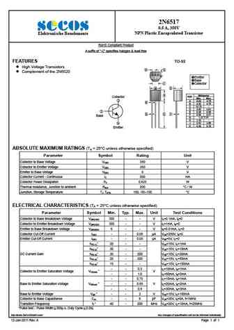
2N6517 0.5 A, 350V NPN Plastic Encapsulated Transistor Elektronische Bauelemente RoHS Compliant Product A suffix of -C specifies halogen & lead-free FEATURES TO-92 High Voltage Transistors G H Complement of the 2N6520 Emitter Base J Collector A D Millimeter B REF. Collector Min. Max. A 4.40 4.70 K B 4.30 4.70 C 12.70 - D 3.30 3.8
ssd02n65.pdf
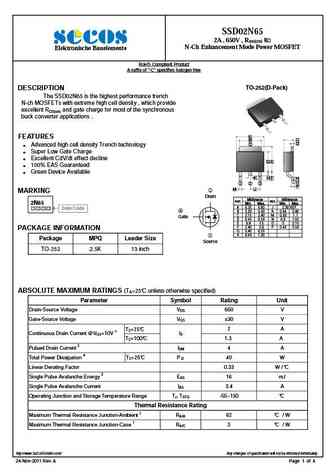
SSD02N65 2A , 650V , RDS(ON) 8 N-Ch Enhancement Mode Power MOSFET Elektronische Bauelemente RoHS Compliant Product A suffix of -C specifies halogen free TO-252(D-Pack) DESCRIPTION The SSD02N65 is the highest performance trench N-ch MOSFETs with extreme high cell density , which provide excellent RDS(on) and gate charge for most of the synchronous buck converter ap
2n6494 2n6594.pdf
A Boca Semiconductor Corp http //www.bocasemi.com A Boca Semiconductor Corp BSC http //www.bocasemi.com A Boca Semiconductor Corp BSC http //www.bocasemi.com
2n6515-7 9 2n6520.pdf
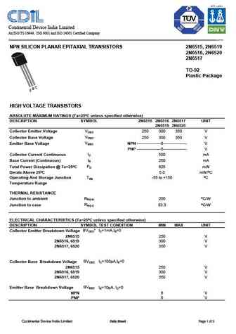
Continental Device India Limited An ISO/TS 16949, ISO 9001 and ISO 14001 Certified Company NPN SILICON PLANAR EPITAXIAL TRANSISTORS 2N6515, 2N6519 2N6516, 2N6520 2N6517 TO-92 Plastic Package HIGH VOLTAGE TRANSISTORS ABSOLUTE MAXIMUM RATINGS (Ta=25 C unless specified otherwise) DESCRIPTION SYMBOL 2N6515 2N6516 2N6517 UNIT 2N6519 2N6520 VCEO Collector Emitter Voltage 250 300 350 V V
2n657.pdf
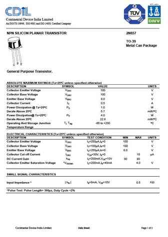
Continental Device India Limited An ISO/TS 16949, ISO 9001 and ISO 14001 Certified Company NPN SILICON PLANAR TRANSISTOR 2N657 TO-39 Metal Can Package General Purpose Transistor. ABSOLUTE MAXIMUM RATINGS (Ta=25 C unless specified otherwise) DESCRIPTION SYMBOL VALUE UNITS VCEO Collector Emitter Voltage 100 V VCBO Collector Base Voltage 100 V VEBO Emitter Base Voltage 8.0 V IC Col
cjd02n65.pdf
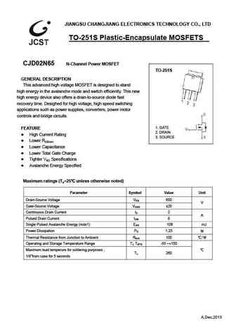
JIANGSU CHANGJIANG ELECTRONICS TECHNOLOGY CO., LTD TO-251S Plastic-Encapsulate MOSFETS CJD02N65 N-Channel Power MOSFET TO-251S GENERAL DESCRIPTION This advanced high voltage MOSFET is designed to stand high energy in the avalanche mode and switch efficiently. This new high energy device also offers a drain-to-source diode fast recovery time. Desighed for high voltage, high sp
cjp02n65.pdf
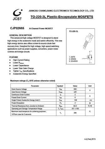
JIANGSU CHANGJIANG ELECTRONICS TECHNOLOGY CO., LTD TO-220-3L Plastic-Encapsulate MOSFETS CJP02N65 N-Channel Power MOSFET TO-220-3L GENERAL DESCRIPTION This advanced high voltage MOSFET is designed to stand high energy in the avalanche mode and switch efficiently. This new high energy device also offers a drain-to-source diode fast recovery time. Desighed for high voltage, hig
cju02n65.pdf
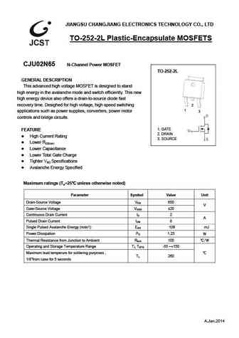
JIANGSU CHANGJIANG ELECTRONICS TECHNOLOGY CO., LTD TO-252-2L Plastic-Encapsulate MOSFETS CJU02N65 N-Channel Power MOSFET TO-252-2L GENERAL DESCRIPTION This advanced high voltage MOSFET is designed to stand high energy in the avalanche mode and switch efficiently. This new high energy device also offers a drain-to-source diode fast recovery time. Desighed for high voltage, hig
2n6520.pdf
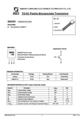
JIANGSU CHANGJING ELECTRONICS TECHNOLOGY CO., LTD TO-92 Plastic-Encapsulate Transistors TO 92 2N6520 TRANSISTOR (PNP) 1. EMITTER FEATURES 2. BASE Complement to 2N6517 3. COLLECTOR Equivalent Circuit 2N6520=Device code Solid dot=Green molding compound device, if none,the normal device XXX=Code
cjb02n65.pdf
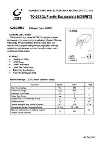
JIANGSU CHANGJIANG ELECTRONICS TECHNOLOGY CO., LTD TO-263-2L Plastic-Encapsulate MOSFETS CJB02N65 N-Channel Power MOSFET TO-263-2L GENERAL DESCRIPTION This advanced high voltage MOSFET is designed to stand high energy in the avalanche mode and switch efficiently. This new high energy device also offers a drain-to-source diode fast recovery time. Desighed for high voltage, hig
cjpf02n65.pdf
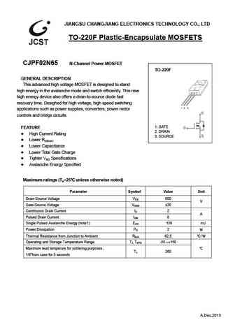
JIANGSU CHANGJIANG ELECTRONICS TECHNOLOGY CO., LTD TO-220F Plastic-Encapsulate MOSFETS CJPF02N65 N-Channel Power MOSFET TO-220F GENERAL DESCRIPTION This advanced high voltage MOSFET is designed to stand high energy in the avalanche mode and switch efficiently. This new high energy device also offers a drain-to-source diode fast recovery time. Desighed for high voltage, high s
cjp12n65.pdf
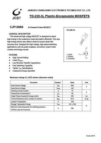
JIANGSU CHANGJIANG ELECTRONICS TECHNOLOGY CO., LTD TO-220-3L Plastic-Encapsulate MOSFETS CJP12N65 N-Channel Power MOSFET TO-220-3L GENERAL DESCRIPTION This advanced high voltage MOSFET is designed to stand high energy in the avalanche mode and switch efficiently. This new high energy device also offers a drain-to-source diode fast recovery time. Designed for high voltage, hig
2n6517.pdf
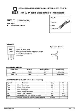
JIANGSU CHANGJING ELECTRONICS TECHNOLOGY CO., LTD TO-92 Plastic-Encapsulate Transistors TO 92 2N6517 TRANSISTOR (NPN) 1. EMITTER FEATURES 2. BASE Complement to 2N6520 3. COLLECTOR Equivalent Circuit
cjpf12n65.pdf
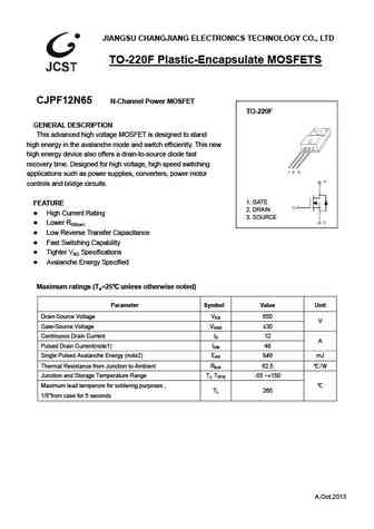
JIANGSU CHANGJIANG ELECTRONICS TECHNOLOGY CO., LTD TO-220F Plastic-Encapsulate MOSFETS CJPF12N65 N-Channel Power MOSFET TO-220F GENERAL DESCRIPTION This advanced high voltage MOSFET is designed to stand high energy in the avalanche mode and switch efficiently. This new high energy device also offers a drain-to-source diode fast recovery time. Designed for high voltage, high s
2n6594.pdf
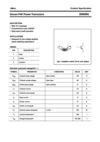
JMnic Product Specification Silicon PNP Power Transistors 2N6594 DESCRIPTION With TO-3 package Complement to type 2N6569 Wide area of safe operation APPLICATIONS Designed for low voltage amplifier power switching applications PINNING PIN DESCRIPTION 1 Base 2 Emitter Fig.1 simplified outline (TO-3) and symbol 3 Collector Absolute maximum ratings(Ta= ) SYMBOL
2n6543.pdf
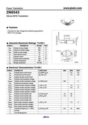
Power Transistors www.jmnic.com 2N6543 Silicon NPN Transistors Features Intended for high voltage,fast switching applications With TO-3 package Absolute Maximum Ratings Tc=25 SYMBOL PARAMETER RATING UNIT VCBO Collector to base voltage 850 V VCEO Collector to emitter voltage 400 V VEBO Emitter to base voltage 9.0 V ICP Peak collector current 16 A IC Collector current 5.0 A P
2n6534.pdf

JMnic Product Specification Silicon NPN Power Transistors 2N6534 DESCRIPTION With TO-66 package DARLINGTON APPLICATIONS Power switching Hammer drivers Series and shunt regulators Audio amplifiers PINNING (See Fig.2) PIN DESCRIPTION 1 Base 2 Emitter Fig.1 simplified outline (TO-66) and symbol 3 Collector Absolute maximum ratings(Ta=25 ) SYMBOL PARAMET
2n6533.pdf
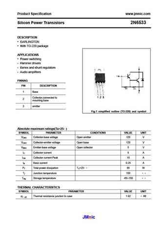
Product Specification www.jmnic.com Silicon Power Transistors 2N6533 DESCRIPTION DARLINGTON With TO-220 package APPLICATIONS Power switching Hammer drivers Series and shunt regulators Audio amplifiers PINNING PIN DESCRIPTION 1 Base Collector;connected to 2 mounting base 3 emitter Fig.1 simplified outline (TO-220) and symbol Absolute maximum ratings(
2n6536.pdf
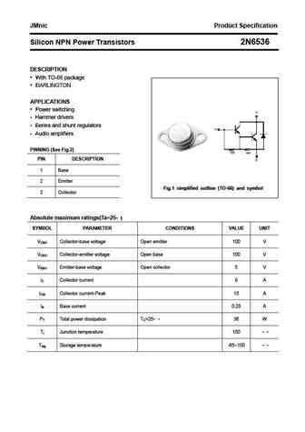
JMnic Product Specification Silicon NPN Power Transistors 2N6536 DESCRIPTION With TO-66 package DARLINGTON APPLICATIONS Power switching Hammer drivers Series and shunt regulators Audio amplifiers PINNING (See Fig.2) PIN DESCRIPTION 1 Base 2 Emitter Fig.1 simplified outline (TO-66) and symbol 3 Collector Absolute maximum ratings(Ta=25 ) SYMBOL PARAMET
2n6546.pdf
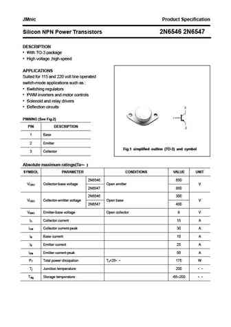
JMnic Product Specification Silicon NPN Power Transistors 2N6546 2N6547 DESCRIPTION With TO-3 package High voltage ,high speed APPLICATIONS Suited for 115 and 220 volt line operated switch-mode applications such as Switching regulators PWM inverters and motor controls Solenoid and relay drivers Deflection circuits PINNING (See Fig.2) PIN DESCRIPTION 1 Ba
2n6535.pdf
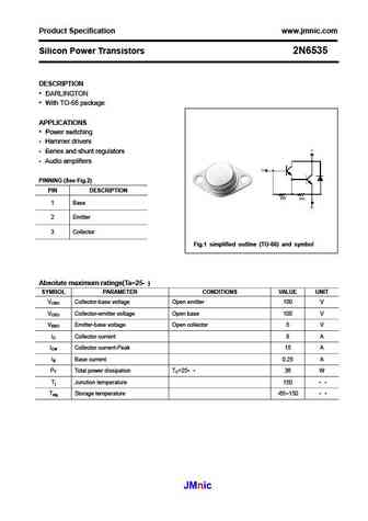
Product Specification www.jmnic.com Silicon Power Transistors 2N6535 DESCRIPTION DARLINGTON With TO-66 package APPLICATIONS Power switching Hammer drivers Series and shunt regulators Audio amplifiers PINNING (See Fig.2) PIN DESCRIPTION 1 Base 2 Emitter 3 Collector Fig.1 simplified outline (TO-66) and symbol Absolute maximum ratings(Ta=25 ) SYMBOL PAR
2n6542.pdf
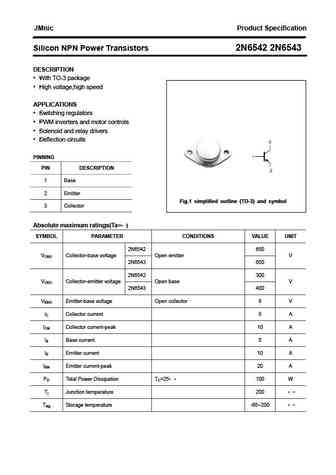
JMnic Product Specification Silicon NPN Power Transistors 2N6542 2N6543 DESCRIPTION With TO-3 package High voltage,high speed APPLICATIONS Switching regulators PWM inverters and motor controls Solenoid and relay drivers Deflection circuits PINNING PIN DESCRIPTION 1 Base 2 Emitter Fig.1 simplified outline (TO-3) and symbol 3 Collector Absolute maximum rat
2n6547.pdf
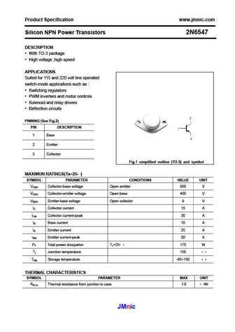
Product Specification www.jmnic.com Silicon NPN Power Transistors 2N6547 DESCRIPTION With TO-3 package High voltage ,high speed APPLICATIONS Suited for 115 and 220 volt line operated switch-mode applications such as Switching regulators PWM inverters and motor controls Solenoid and relay drivers Deflection circuits PINNING (See Fig.2) PIN DESCRIPTION 1 Ba
2n6576 2n7577 2n7578.pdf
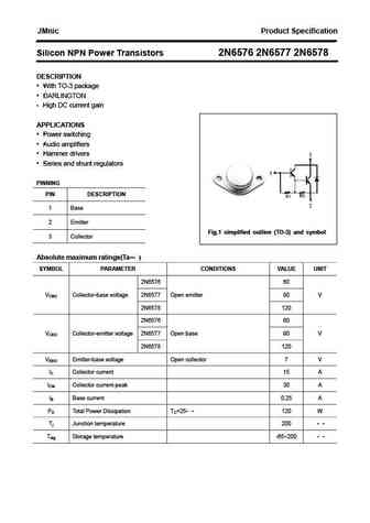
JMnic Product Specification Silicon NPN Power Transistors 2N6576 2N6577 2N6578 DESCRIPTION With TO-3 package DARLINGTON High DC current gain APPLICATIONS Power switching Audio amplifiers Hammer drivers Series and shunt regulators PINNING PIN DESCRIPTION 1 Base 2 Emitter Fig.1 simplified outline (TO-3) and symbol 3 Collector Absolute maximum ratings(T
2n6537.pdf

JMnic Product Specification Silicon NPN Power Transistors 2N6537 DESCRIPTION With TO-66 package DARLINGTON APPLICATIONS Power switching Hammer drivers Series and shunt regulators Audio amplifiers PINNING (See Fig.2) PIN DESCRIPTION 1 Base 2 Emitter Fig.1 simplified outline (TO-66) and symbol 3 Collector Absolute maximum ratings(Ta=25 ) SYMBOL PARAMET
2n6569.pdf
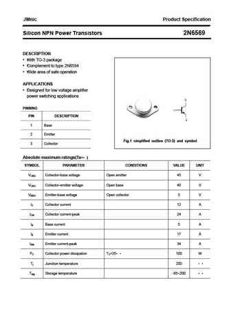
JMnic Product Specification Silicon NPN Power Transistors 2N6569 DESCRIPTION With TO-3 package Complement to type 2N6594 Wide area of safe operation APPLICATIONS Designed for low voltage amplifier power switching applications PINNING PIN DESCRIPTION 1 Base 2 Emitter Fig.1 simplified outline (TO-3) and symbol 3 Collector Absolute maximum ratings(Ta= ) SYMBO
cep02n65a ceb02n65a cef02n65a.pdf
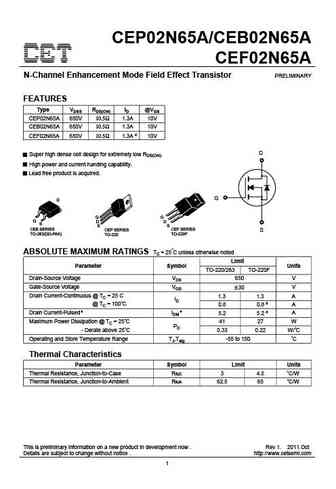
CEP02N65A/CEB02N65A CEF02N65A N-Channel Enhancement Mode Field Effect Transistor PRELIMINARY FEATURES Type VDSS RDS(ON) ID @VGS CEP02N65A 650V 10.5 1.3A 10V CEB02N65A 650V 10.5 1.3A 10V CEF02N65A 650V 10.5 1.3A d 10V D Super high dense cell design for extremely low RDS(ON). High power and current handing capability. Lead free product is acquired. G CEB SERIES CEP SERIES C
ceu02n65g ced02n65g.pdf
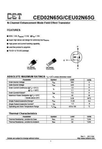
CED02N65G/CEU02N65G N-Channel Enhancement Mode Field Effect Transistor FEATURES 650V, 1.8A, RDS(ON) = 5.5 @VGS = 10V. Super high dense cell design for extremely low RDS(ON). High power and current handing capability. D Lead free product is acquired. TO-251 & TO-252 package. D G G S CEU SERIES CED SERIES S TO-252(D-PAK) TO-251(I-PAK) ABSOLUTE MAXIMUM RATINGS Tc = 25 C unless
ceu02n65a ced02n65a.pdf
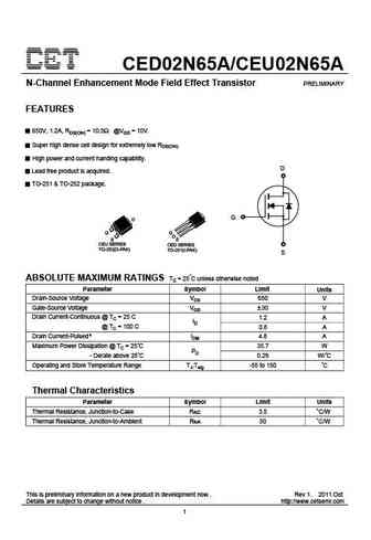
CED02N65A/CEU02N65A N-Channel Enhancement Mode Field Effect Transistor PRELIMINARY FEATURES 650V, 1.2A, RDS(ON) = 10.5 @VGS = 10V. Super high dense cell design for extremely low RDS(ON). High power and current handing capability. D Lead free product is acquired. TO-251 & TO-252 package. G D G S CEU SERIES CED SERIES TO-252(D-PAK) TO-251(I-PAK) S ABSOLUTE MAXIMUM RATINGS Tc
cep02n65g ceb02n65g cef02n65g.pdf
CEP02N65G/CEB02N65G CEF02N65G N-Channel Enhancement Mode Field Effect Transistor FEATURES Type VDSS RDS(ON) ID @VGS CEP02N65G 650V 5.5 2A 10V CEB02N65G 650V 5.5 2A 10V CEF02N65G 650V 5.5 2A d 10V D Super high dense cell design for extremely low RDS(ON). High power and current handing capability. Lead free product is acquired. G S CEB SERIES CEP SERIES CEF SERIES TO-263(
ceef02n65g.pdf
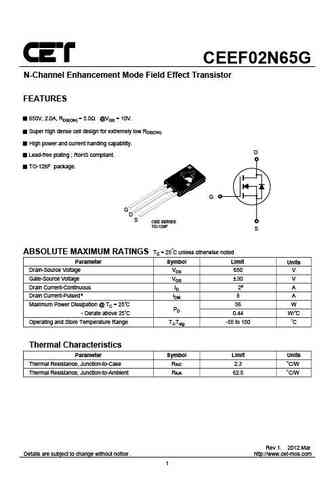
CEEF02N65G N-Channel Enhancement Mode Field Effect Transistor FEATURES 650V, 2.0A, RDS(ON) = 5.0 @VGS = 10V. Super high dense cell design for extremely low RDS(ON). High power and current handing capability. D Lead-free plating ; RoHS compliant. TO-126F package. G G D S CEE SERIES TO-126F S ABSOLUTE MAXIMUM RATINGS Tc = 25 C unless otherwise noted Parameter Symbol Limit Unit
cep12n65 ceb12n65 cef12n65.pdf
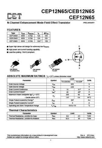
CEP12N65/CEB12N65 CEF12N65 PRELIMINARY N-Channel Enhancement Mode Field Effect Transistor FEATURES Type VDSS RDS(ON) ID @VGS CEP12N65 650V 0.73 12A 10V CEB12N65 650V 0.73 12A 10V CEF12N65 650V 0.73 12A d 10V D Super high dense cell design for extremely low RDS(ON). High power and current handing capability. Lead-free plating ; RoHS compliant. G S CEB SERIES CEP SERIES C
wnm12n65-f.pdf
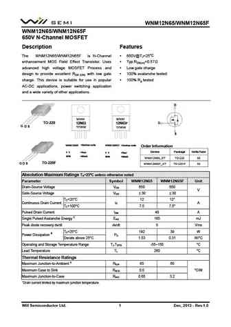
WNM12N65/WNM12N65F WNM12N65/WNM12N65F 650V N-Channel MOSFET Description Features C The WNM12N65/WNM12N65F is N-Channel 650V@TJ=25 enhancement MOS Field Effect Transistor. Uses Typ.RDS(on)=0.57 advanced high voltage MOSFET Process and Low gate charge design to provide excellent RDS (ON) with low gate 100% avalanche tested charge. This device is suitable for use in p
h12n65.pdf
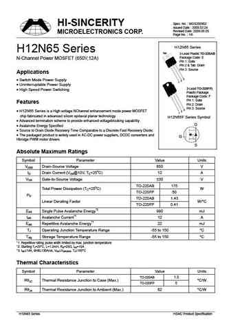
Spec. No. MOS200902 HI-SINCERITY Issued Date 2009.03.24 Revised Date 2009.08.05 MICROELECTRONICS CORP. Page No. 1/6 H12N65 Series H12N65 Series Tab 3-Lead Plastic TO-220AB Package Code E N-Channel Power MOSFET (650V,12A) Pin 1 Gate Pin 2 & Tab Drain Pin 3 Source Applications 3 Switch Mode Power Supply 2 1 Uninterruptable Power Supply 3-L
h02n65.pdf
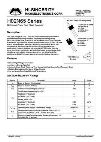
Spec. No. MOS200910 HI-SINCERITY Issued Date 2009.04.07 Revised Date MICROELECTRONICS CORP. Page No. 1/6 H02N65 Series Pin Assignment H02N65 Series Tab 3-Lead Plastic TO-220AB N-Channel Power Field Effect Transistor Package Code E Pin 1 Gate Pin 2 & Tab Drain Pin 3 Source Description 3 2 This high voltage MOSFET uses an advanced termination scheme to
aob12n65l.pdf

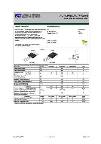
AOT12N65/AOTF12N65/AOB12N65 650V, 12A N-Channel MOSFET General Description Product Summary VDS 750V@150 The AOT12N65 & AOTF12N65 & AOB12N65 have been fabricated using an advanced high voltage MOSFET ID (at VGS=10V) 12A process that is designed to deliver high levels of RDS(ON) (at VGS=10V)
aotf12n65.pdf
AOT12N65/AOTF12N65 650V, 12A N-Channel MOSFET General Description Product Summary VDS 750V@150 The AOT12N65 & AOTF12N65 have been fabricated using an advanced high voltage MOSFET process that is ID (at VGS=10V) 12A designed to deliver high levels of performance and RDS(ON) (at VGS=10V)
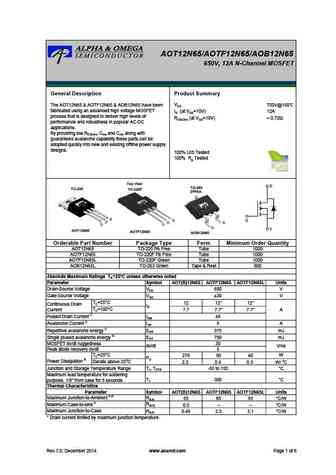
aot12n65 aotf12n65 aotf12n65l aob12n65l.pdf

AOT12N65/AOTF12N65/AOTF12N65L/AOB12N65L 650V, 12A N-Channel MOSFET General Description Product Summary VDS 750V@150 The AOT12N65 & AOTF12N65 & AOTF12N65L & AOB12N65L have been fabricated using an advanced ID (at VGS=10V) 12A high voltage MOSFET process that is designed to deliver RDS(ON) (at VGS=10V)
aot12n65 aotf12n65 aob12n65.pdf
AOT12N65/AOTF12N65/AOB12N65 650V, 12A N-Channel MOSFET General Description Product Summary VDS 750V@150 The AOT12N65 & AOTF12N65 & AOB12N65 have been fabricated using an advanced high voltage MOSFET ID (at VGS=10V) 12A process that is designed to deliver high levels of RDS(ON) (at VGS=10V)
aowf12n65.pdf
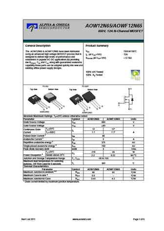
AOW12N65/AOWF12N65 650V, 12A N-Channel MOSFET General Description Product Summary VDS 750V@150 The AOW12N65 & AOWF12N65 have been fabricated using an advanced high voltage MOSFET process that is ID (at VGS=10V) 12A designed to deliver high levels of performance and RDS(ON) (at VGS=10V)
aow12n65 aowf12n65.pdf

AOW12N65/AOWF12N65 650V, 12A N-Channel MOSFET General Description Product Summary VDS 750V@150 The AOW12N65 & AOWF12N65 have been fabricated using an advanced high voltage MOSFET process that is ID (at VGS=10V) 12A designed to deliver high levels of performance and RDS(ON) (at VGS=10V)
aow12n65.pdf

AOW12N65/AOWF12N65 650V, 12A N-Channel MOSFET General Description Product Summary VDS 750V@150 The AOW12N65 & AOWF12N65 have been fabricated using an advanced high voltage MOSFET process that is ID (at VGS=10V) 12A designed to deliver high levels of performance and RDS(ON) (at VGS=10V)
aot12n65.pdf

AOT12N65/AOTF12N65 650V, 12A N-Channel MOSFET General Description Product Summary VDS 750V@150 The AOT12N65 & AOTF12N65 have been fabricated using an advanced high voltage MOSFET process that is ID (at VGS=10V) 12A designed to deliver high levels of performance and RDS(ON) (at VGS=10V)
am12n65pcfm.pdf
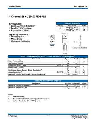
Analog Power AM12N65PCFM N-Channel 650-V (D-S) MOSFET PRODUCT SUMMARY Key Features rDS(on) (m ) VDS (V) ID (A) Low r trench technology DS(on) 800 @ VGS = 10V 7 Low thermal impedance 650 850 @ VGS = 6V 6.5 Fast switching speed Typical Applications Power Supplies Motor Drives Consumer Electronics ABSOLUTE MAXIMUM RATINGS (TA = 25 C UNLESS OTH
am12n65p.pdf
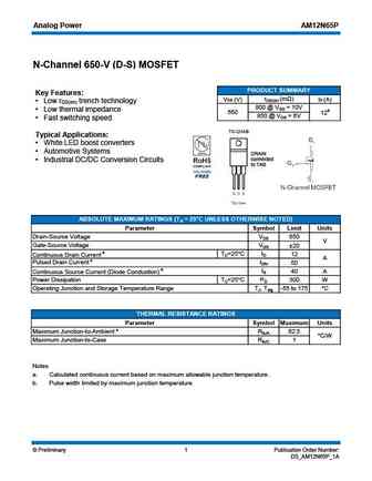
Analog Power AM12N65P N-Channel 650-V (D-S) MOSFET PRODUCT SUMMARY Key Features rDS(on) (m ) VDS (V) ID (A) Low r trench technology DS(on) 800 @ VGS = 10V Low thermal impedance 650 12a 850 @ VGS = 6V Fast switching speed Typical Applications White LED boost converters Automotive Systems DRAIN connected Industrial DC/DC Conversion Circuits
afn12n65t220ft afn12n65t220t.pdf
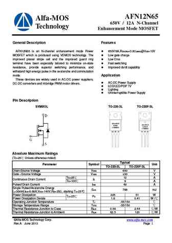
AFN12N65 Alfa-MOS 650V / 12A N-Channel Technology Enhancement Mode MOSFET General Description Features AFN12N65 is an N-channel enhancement mode Power 650V/6A,RDS(ON)=0.8 (MAX)@VGS=10V MOSFET which is produced using VDMOS technology. The Low gate charge improved planar stripe cell and the improved guard ring Low Crss terminal have been especially tailored to minimize on-stat
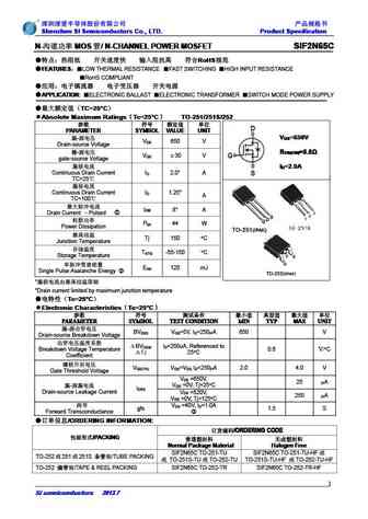
sif2n65c 1.pdf
Shenzhen SI Semiconductors Co., LTD. Product Specification Shenzhen SI Semiconductors Co., LTD. Product Specification Shenzhen SI Semiconductors Co., LTD. Product Specification Shenzhen SI Semiconductors Co., LTD. Product Specification N- MOS / N-CHANNEL POWER MOSFET SIF2N65C N- MOS / N-CHANNEL POWER MOSFET SIF2N65C N- MOS / N-CHANN
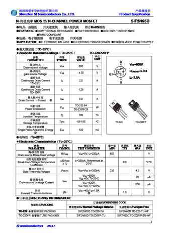
sif2n65d.pdf
Shenzhen SI Semiconductors Co., LTD. Product Specification Shenzhen SI Semiconductors Co., LTD. Product Specification Shenzhen SI Semiconductors Co., LTD. Product Specification Shenzhen SI Semiconductors Co., LTD. Product Specification N- MOS / N-CHANNEL POWER MOSFET SIF2N65D N- MOS / N-CHANNEL POWER MOSFET SIF2N65D N- MOS / N-CHANN
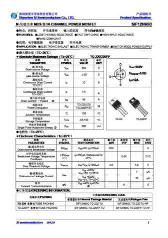
sif12n65c.pdf
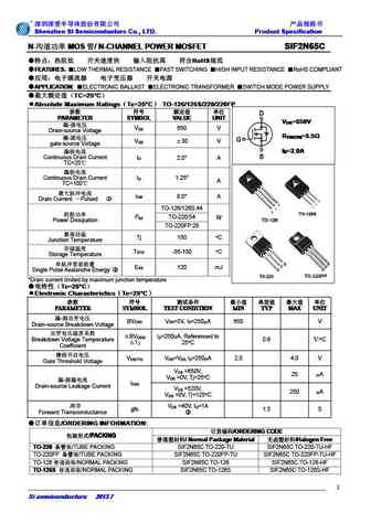
Shenzhen SI Semiconductors Co., LTD. Product Specification Shenzhen SI Semiconductors Co., LTD. Product Specification Shenzhen SI Semiconductors Co., LTD. Product Specification Shenzhen SI Semiconductors Co., LTD. Product Specification N- MOS / N-CHANNEL POWER MOSFET SIF12N65C N- MOS / N-CHANNEL POWER MOSFET SIF12N65C
sif2n65c.pdf
Shenzhen SI Semiconductors Co., LTD. Product Specification Shenzhen SI Semiconductors Co., LTD. Product Specification Shenzhen SI Semiconductors Co., LTD. Product Specification Shenzhen SI Semiconductors Co., LTD. Product Specification N- MOS / N-CHANNEL POWER MOSFET SIF2N65C N- MOS / N-CHANNEL POWER MOSFET SIF2N65C N- MOS / N-CHANN
jcs12n65fei jcs12n65bei jcs12n65sei jcs12n65cei.pdf
N R N-CHANNEL MOSFET JCS12N65EI Package MAIN CHARACTERISTICS ID 12A VDSS 650V Rdson-max 0.9 Vgs=10V Qg-Typ 30nC APPLICATIONS High efficiency switch mode power supplies Electronic lamp ballasts LED based on half bridge LE
jcs2n65vb jcs2n65rb jcs2n65cb jcs2n65fb jcs2n65mb jcs2n65mfb.pdf
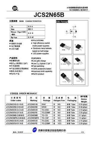
N R N-CHANNEL MOSFET JCS2N65B MAIN CHARACTERISTICS Package ID 2.0 A VDSS 650 V Rdson Vgs=10V 5.0 -MAX Qg-typ 5.9 nC APPLICATIONS High efficiency switch mode power supplies Electronic lamp ballasts LED based on half bridge
jcs12n65bt jcs12n65st jcs12n65ct jcs12n65ft.pdf
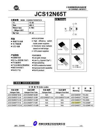
N R N-CHANNEL MOSFET JCS12N65T Package MAIN CHARACTERISTICS ID 12.0A VDSS 650 V Rdson-max 0.78 @Vgs=10V Qg-typ 39 nC APPLICATIONS High efficiency switch mode power supplies Electronic lamp ballasts LED based on half bridge
jcs2n65v jcs2n65r jcs2n65c jcs2n65f.pdf
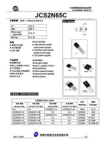
N R N-CHANNEL MOSFET JCS2N65C MAIN CHARACTERISTICS Package ID 2.0 A VDSS 650 V Rdson_max 5.5 Vgs=10V Qg-typ 8.4 nC APPLICATIONS High efficiency switch mode power supplies Electronic lamp ballasts LED based on half bridge
jcs2n65e.pdf
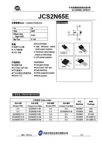
N R N-CHANNEL MOSFET JCS2N65E Package MAIN CHARACTERISTICS ID 2A VDSS 650V Rdson-max 5.5 Vgs=10V Qg-Typ 6.7nC APPLICATIONS High efficiency switch mode power supplies Electronic lamp ballasts LED based on half bridge LED p
jcs2n65fc.pdf
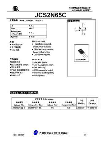
N R N-CHANNEL MOSFET JCS2N65C MAIN CHARACTERISTICS Package ID 2.0 A VDSS 650 V Rdson_max 5.5 Vgs=10V Qg-typ 8.4 nC APPLICATIONS High efficiency switch mode power supplies Electronic lamp ballasts LED based on half bridge
mtn12n65fp.pdf
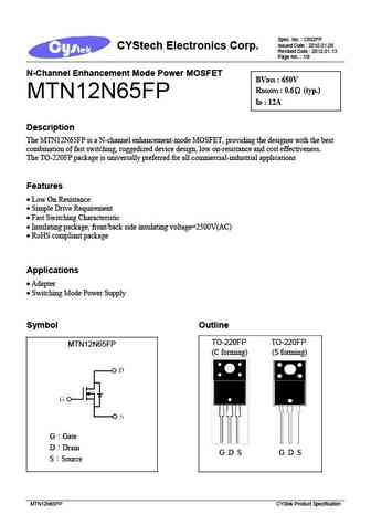
Spec. No. C802FP Issued Date 2010.01.08 CYStech Electronics Corp. Revised Date 2012.01.13 Page No. 1/9 N-Channel Enhancement Mode Power MOSFET BVDSS 650V RDS(ON) 0.6 (typ.) MTN12N65FP ID 12A Description The MTN12N65FP is a N-channel enhancement-mode MOSFET, providing the designer with the best combination of fast switching, ruggedized device design, low on
mtn2n65j3.pdf
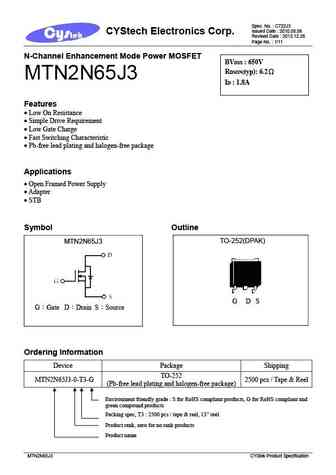
Spec. No. C722J3 Issued Date 2010.08.06 CYStech Electronics Corp. Revised Date 2013.12.26 Page No. 1/11 N-Channel Enhancement Mode Power MOSFET BVDSS 650V RDSON(typ) 6.2 MTN2N65J3 ID 1.8A Features Low On Resistance Simple Drive Requirement Low Gate Charge Fast Switching Characteristic Pb-free lead plating and halogen-free package
mtn2n65i3.pdf
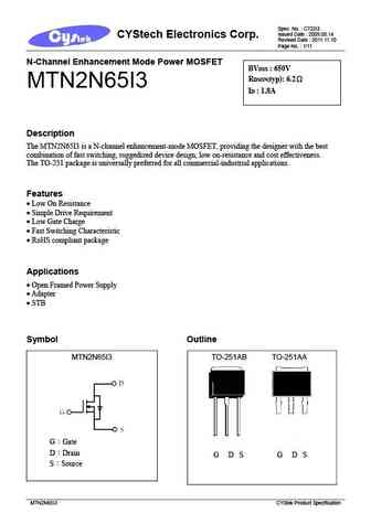
Spec. No. C722I3 Issued Date 2009.08.14 CYStech Electronics Corp. Revised Date 2011.11.10 Page No. 1/11 N-Channel Enhancement Mode Power MOSFET BVDSS 650V RDSON(typ) 6.2 MTN2N65I3 ID 1.8A Description The MTN2N65I3 is a N-channel enhancement-mode MOSFET, providing the designer with the best combination of fast switching, ruggedized device design, low on-resi
mtn2n65fp.pdf
Spec. No. C722FP Issued Date 2010.03.15 CYStech Electronics Corp. Revised Date 2012.11.08 Page No. 1/10 N-Channel Enhancement Mode Power MOSFET BVDSS 650V RDS(ON) 5.8 (typ.) MTN2N65FP ID 1.8A Description The MTN2N65FP is a N-channel enhancement-mode MOSFET, providing the designer with the best combination of fast switching, ruggedized device design, low on-
mtn2n65ai3.pdf
Spec. No. C799I3 Issued Date 2010.03.29 CYStech Electronics Corp. Revised Date 2011.11.10 Page No. 1/11 N-Channel Enhancement Mode Power MOSFET BVDSS 650V RDSON(typ.) 5.0 MTN2N65AI3 ID 2A Description The MTN2N65AI3 is a N-channel enhancement-mode MOSFET, providing the designer with the best combination of fast switching, ruggedized device design, low on-res
12n65a 12n65af.pdf
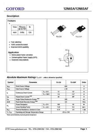
12N65A/12N65AF GOFORD Description Features VDSS RDS(ON) ID @ 10V (typ) 12A 650V 0.65 Fast switching 100% avalanche tested Improved dv/dt capability Application Active power factor correction Uninterruptible Power Supply (UPS) Electronic lamp ballasts Absolute Maximum Ratings TC=25 unless otherwise specified Symbol Parameter TO-220
sdf02n65 sdp02n65.pdf
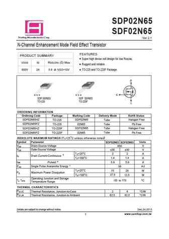
SDP02N65 SDF02N65 a S mHop Microelectronics C orp. Ver 2.1 N-Channel Enhancement Mode Field Effect Transistor FEATURES PRODUCT SUMMARY Super high dense cell design for low RDS(ON). RDS(ON) ( ) Max VDSS ID Rugged and reliable. 650V 2A 5.6 @ VGS=10V TO-220 and TO-220F Package. D G D S G D S G SDP SERIES SDF SERIES TO-220 TO-220F S ORDERING INFORMATION Ordering Code Package Mar
ssf12n65f.pdf
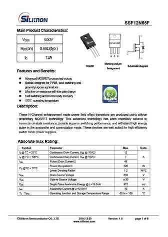
SSF12N65F Main Product Characteristics VDSS 650V RDS(on) 0.68 (typ.) ID 12A Marking and pin TO220F Schematic diagram Assignment Features and Benefits Advanced MOSFET process technology Special designed for PWM, load switching and general purpose applications Ultra low on-resistance with low gate charge Fast switching and reverse body recovery
ftp02n65 fta02n65.pdf
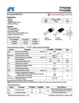
FTP02N65 FTA02N65 N-Channel MOSFET Pb Lead Free Package and Finish Applications Adaptor VDSS RDS(ON) (Max.) ID Charger 650V 5.0 2.0A SMPS Standby Power LCD Panel Power Features D RoHS Compliant Low ON Resistance Low Gate Charge Peak Current vs Pulse Width Curve G G D G Inductive Switching Curves S D S Ordering Information TO-220
ftp02n65b fta02n65b ftq02n65b.pdf
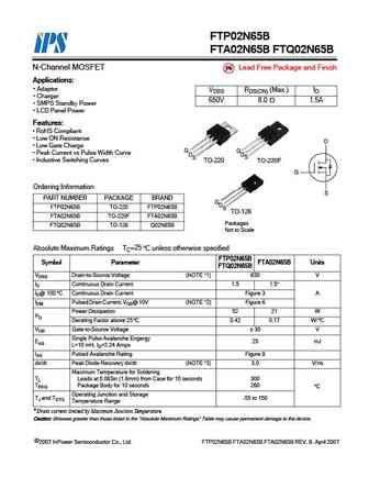
FTP02N65B FTA02N65B FTQ02N65B N-Channel MOSFET Pb Lead Free Package and Finish Applications Adaptor VDSS RDS(ON) (Max.) ID Charger 650V 8.0 1.5A SMPS Standby Power LCD Panel Power Features RoHS Compliant Low ON Resistance D Low Gate Charge G G Peak Current vs Pulse Width Curve DS DS Inductive Switching Curves TO-220 TO-220F G Order
brf12n65.pdf
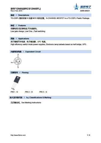
BRF12N65(BRCS12N65FL) Rev.C Feb.-2015 DATA SHEET / Descriptions TO-220FL N MOS N-CHANNEL MOSFET in a TO-220FL Plastic Package. / Features , , Low gate charge, Low Crss , Fast switching. / Applications UPS High efficiency sw
brf2n65.pdf
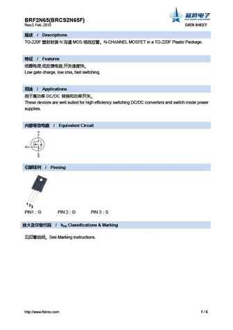
BRF2N65(BRCS2N65F) Rev.C Feb.-2015 DATA SHEET / Descriptions TO-220F N MOS N-CHANNEL MOSFET in a TO-220F Plastic Package. / Features , , Low gate charge, low crss, fast switching. / Applications DC/DC These devices are well suited for hi
brcs12n65bd.pdf
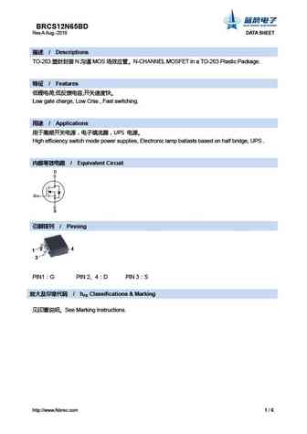
BRCS12N65BD Rev.A Aug.-2018 DATA SHEET / Descriptions TO-263 N MOS N-CHANNEL MOSFET in a TO-263 Plastic Package. / Features , , Low gate charge, Low Crss , Fast switching. / Applications UPS High efficiency switch mode pow
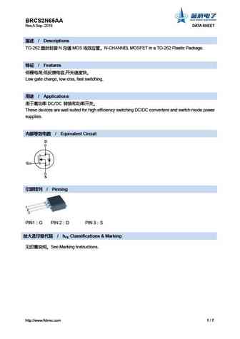
brcs2n65aa.pdf
BRCS2N65AA Rev.A Sep.-2018 DATA SHEET / Descriptions TO-262 N MOS N-CHANNEL MOSFET in a TO-262 Plastic Package. / Features , , Low gate charge, low crss, fast switching. / Applications DC/DC These devices are well suited for high efficie
brcs2n65qf.pdf
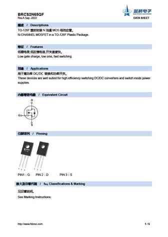
BRCS2N65QF Rev.A Sep.-2022 DATA SHEET / Descriptions TO-126F N MOS N-CHANNEL MOSFET in a TO-126F Plastic Package. / Features , , Low gate charge, low crss, fast switching. / Applications DC/DC These devices are well suited for high eff
brfl12n65.pdf
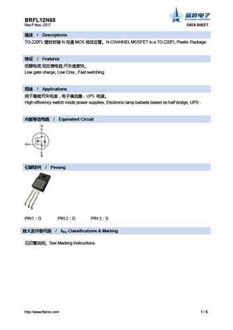
BRFL12N65 Rev.F Nov.-2017 DATA SHEET / Descriptions TO-220FL N MOS N-CHANNEL MOSFET in a TO-220FL Plastic Package. / Features , , Low gate charge, Low Crss , Fast switching. / Applications UPS High efficiency switch mode po
brcs2n65ip.pdf
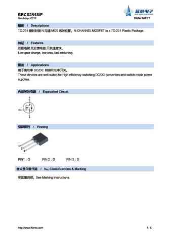
BRCS2N65IP Rev.A Apr.-2018 DATA SHEET / Descriptions TO-251 N MOS N-CHANNEL MOSFET in a TO-251 Plastic Package. / Features , , Low gate charge, low crss, fast switching. / Applications DC/DC These devices are well suited for high efficie
brd2n65.pdf
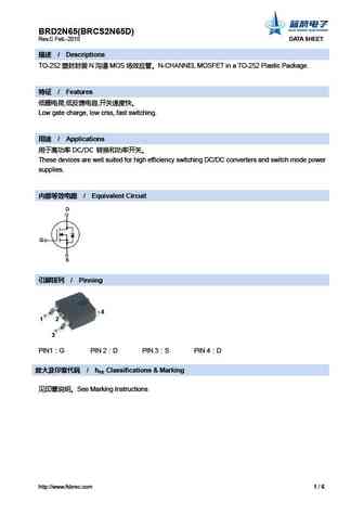
BRD2N65(BRCS2N65D) Rev.C Feb.-2015 DATA SHEET / Descriptions TO-252 N MOS N-CHANNEL MOSFET in a TO-252 Plastic Package. / Features , , Low gate charge, low crss, fast switching. / Applications DC/DC These devices are well suited for high
bri2n65.pdf
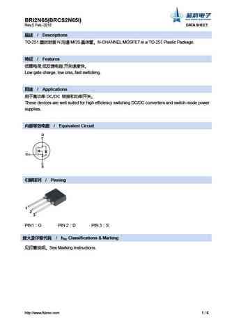
BRI2N65(BRCS2N65I) Rev.C Feb.-2015 DATA SHEET / Descriptions TO-251 N MOS N-CHANNEL MOSFET in a TO-251 Plastic Package. / Features , , Low gate charge, low crss, fast switching. / Applications DC/DC These devices are well suited for high ef
cs2n65 a3.pdf
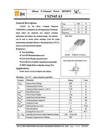
Silicon N-Channel Power MOSFET R CS2N65 A3 General Description VDSS 650 V CS2N65 A3, the silicon N-channel Enhanced ID 2 A PD (TC=25 ) 35 W VDMOSFETs, is obtained by the self-aligned planar Technology RDS(ON)Typ 3.9 which reduce the conduction loss, improve switching performance and enhance the avalanche energy. The transistor can be used in various power swi
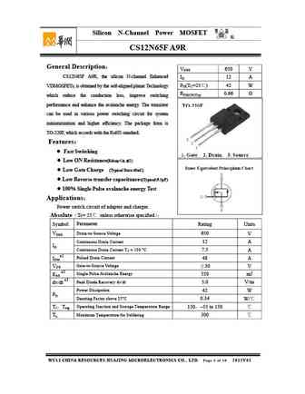
cs12n65f a9r.pdf
Silicon N-Channel Power MOSFET R CS12N65F A9R General Description VDSS 650 V CS12N65F A9R, the silicon N-channel Enhanced ID 12 A PD(TC=25 ) 42 W VDMOSFETs, is obtained by the self-aligned planar Technology RDS(ON)Typ 0.66 which reduce the conduction loss, improve switching performance and enhance the avalanche energy. The transistor can be used in various p
cs2n65 a4hy.pdf

Silicon N-Channel Power MOSFET R CS2N65 A4HY General Description VDSS 650 V CS2N65 A4HY, the silicon N-channel Enhanced ID 2 A PD(TC=25 ) 35 W VDMOSFETs, is obtained by the self-aligned planar Technology RDS(ON)Typ 3.9 which reduce the conduction loss, improve switching performance and enhance the avalanche energy. The transistor can be used in various power
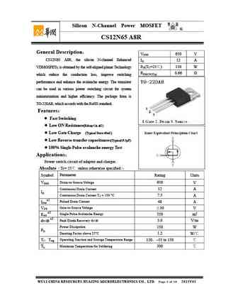
cs12n65 a8r.pdf
Silicon N-Channel Power MOSFET R CS12N65 A8R General Description VDSS 650 V CS12N65 A8R, the silicon N-channel Enhanced ID 12 A PD(TC=25 ) 150 W VDMOSFETs, is obtained by the self-aligned planar Technology RDS(ON)Typ 0.66 which reduce the conduction loss, improve switching performance and enhance the avalanche energy. The transistor can be used in various po
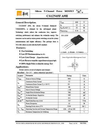
cs12n65f a9h.pdf
Silicon N-Channel Power MOSFET R CS12N65F A9H VDSS 650 V General Description ID 12 A CS12N65F A9H, the silicon N-channel Enhanced PD (TC=25 ) 55 W VDMOSFETs, is obtained by the self-aligned planar RDS(ON)Typ 0.54 Technology which reduce the conduction loss, improve switching performance and enhance the avalanche energy. The transistor can be used in various
cs2n65 a3hy.pdf

Silicon N-Channel Power MOSFET R CS2N65 A3HY General Description VDSS 650 V CS2N65 A3HY, the silicon N-channel Enhanced ID 2 A PD (TC=25 ) 35 W VDMOSFETs, is obtained by the self-aligned planar Technology RDS(ON)Typ 3.9 which reduce the conduction loss, improve switching performance and enhance the avalanche energy. The transistor can be used in various power
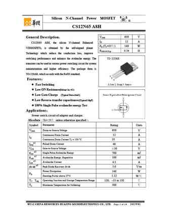
cs12n65 a8h.pdf
Silicon N-Channel Power MOSFET R CS12N65 A8H VDSS 650 V General Description ID 12 A CS12N65 A8H, the silicon N-channel Enhanced PD (TC=25 ) 140 W VDMOSFETs, is obtained by the self-aligned planar RDS(ON)Typ 0.54 Technology which reduce the conduction loss, improve switching performance and enhance the avalanche energy. The transistor can be used in various p
cs2n65f a9hy.pdf

Silicon N-Channel Power MOSFET R CS2N65F A9HY General Description VDSS 650 V CS2N65F A9HY, the silicon N-channel Enhanced ID 2.0 A PD (TC=25 ) 27 W VDMOSFETs, is obtained by the self-aligned planar Technology RDS(ON)Typ 4 which reduce the conduction loss, improve switching performance and enhance the avalanche energy. The transistor can be used in various p
pfp12n65 pff12n65.pdf
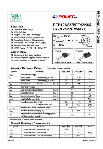
PFP12N65/PFF12N65 FEATURES 650V N-Channel MOSFET Originative New Design 100% EAS Test Rugged Gate Oxide Technology Drain BVDSS = 650 V Extremely Low Intrinsic Capacitances Remarkable Switching Characteristics Gate RDS(on) typ = 0.46 Unequalled Gate Charge 48 nC (Typ.) E
cm12n65a to220a.pdf
R CM12N65A www.jdsemi.cn ShenZhen Jingdao Electronic Co.,Ltd. POWER MOSFET 650V N-Channel VDMOS RoHS 1 LD E 2 3
cm12n65 to220a.pdf
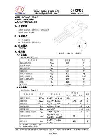
R CM12N65 www.jdsemi.cn ShenZhen Jingdao Electronic Co.,Ltd. POWER MOSFET 650V N-Channel VDMOS RoHS
cm12n65f.pdf
R CM12N65F www.jdsemi.cn ShenZhen Jingdao Electronic Co.,Ltd. POWER MOSFET 650V N-Channel VDMOS RoHS 1 LD E 2 1 2
cm2n65f.pdf
R CM2N65F www.jdsemi.cn ShenZhen Jingdao Electronic Co.,Ltd. POWER MOSFET 650V N-Channel VDMOS RoHS
ftk2n65p f d i.pdf
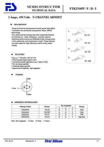
SEMICONDUCTOR FTK2N65P / F / D / I TECHNICAL DATA 2 Amps, 650 Volts N-CHANNEL MOSFET DESCRIPTION These N-Channel enhancement mode power field effect Transistors are produced using planar stripe, DMOS I technology. 1 This advanced technology has been especially tailored TO - 251 to minimize on - state resistance , provide superior switching performance,and Withstand high energy
2n6520.pdf
SEMICONDUCTOR 2N6520 TECHNICAL DATA B C 2N6520 TRANSISTOR (PNP) DIM MILLIMETERS FEATURES A 4.70 MAX E B 4.80 MAX G C 3.70 MAX Complement to 2N6517 D D 0.55 MAX E 1.00 F 1.27 G 0.85 H 0.45 _ H J 14.00 0.50 L 2.30 F F M 0.51 MAX 1 2 3 1. EMITTER 2. BASE 3. COLLECTOR MAXIMUM RATINGS (Ta=25 unless otherwise noted) TO-92 Symbol Parameter Value Unit VCBO Collect
ftk12n65p f dd.pdf
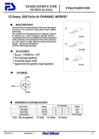
SEMICONDUCTOR FTK12N65P/F/DD TECHNICAL DATA 12 Amps, 650 Volts N-CHANNEL MOSFET DESCRIPTION These N-Channel enhancement mode power field effect P Transistors are produced using planar stripe, DMOS technology. 1 This advanced technology has been especially tailored to minimize on - state resistance , provide superior TO-220 switching performance,and Withstand high energy pulse i
2n6517.pdf
SEMICONDUCTOR 2N6517 TECHNICAL DATA B C 2N6517 TRANSISTOR (NPN) DIM MILLIMETERS A 4.70 MAX E FEATURES G B 4.80 MAX C 3.70 MAX D Complement To 2N6520 D 0.55 MAX E 1.00 F 1.27 G 0.85 H 0.45 _ H J 14.00 0.50 L 2.30 F F M 0.51 MAX 1 2 3 1. EMITTER 2. BASE 3. COLLECTOR TO-92 MAXIMUM RATINGS (Ta=25 unless otherwise noted) Symbol Parameter Value Unit VCBO Collecto
f12n65.pdf
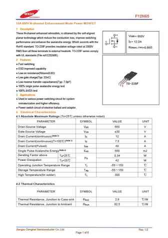
F12N65 12A 650V N-channel Enhancement Mode Power MOSFET 1 Description These N-channel enhanced vdmosfets, is obtained by the self-aligned V DSS = 650V planar technology which reduce the conduction loss, improve switching I = 12.0A D performance and enhance the avalanche energy. Which accords with the RoHS standard. TO-220F provides insulation voltage rated at 2000V R DS(on) TYP)
b2n65.pdf
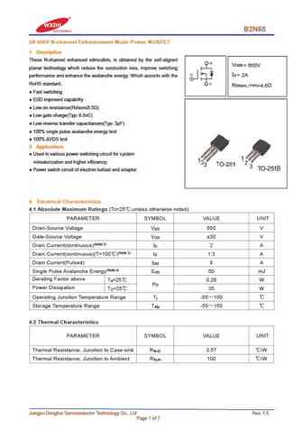
B2N65 2A 650V N-channel Enhancement Mode Power MOSFET 1 Description These N-channel enhanced vdmosfets, is obtained by the self-aligned V DSS = 650V planar technology which reduce the conduction loss, improve switching I = 2A D performance and enhance the avalanche energy. Which accords with the RoHS standard. R DS(on) TYP) =4.6 Fast switching ESD improved capability
12n65.pdf
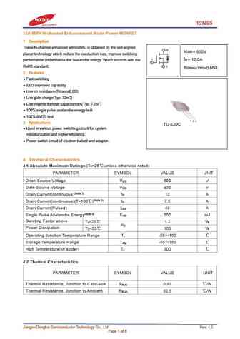
12N65 12A 650V N-channel Enhancement Mode Power MOSFET 1 Description These N-channel enhanced vdmosfets, is obtained by the self-aligned V DSS = 650V planar technology which reduce the conduction loss, improve switching I = 12.0A D performance and enhance the avalanche energy. Which accords with the RoHS standard. R DS(on) TYP) =0.66 2 Features Fast switching ESD imp
d2n65.pdf
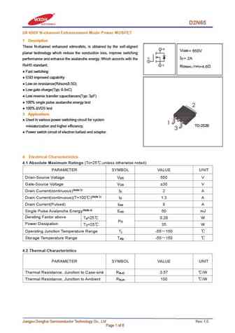
D2N65 2A 650V N-channel Enhancement Mode Power MOSFET 1 Description These N-channel enhanced vdmosfets, is obtained by the self-aligned V DSS = 650V planar technology which reduce the conduction loss, improve switching I = 2A D performance and enhance the avalanche energy. Which accords with the RoHS standard. R DS(on) TYP) =4.6 Fast switching ESD improved capability
kx12n65f.pdf
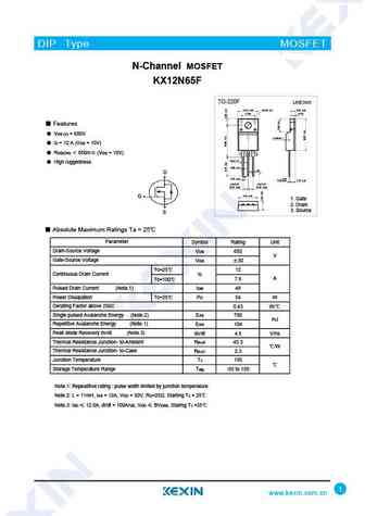
DIP Type MOSFET N-Channel MOSFET KX12N65F TO-220F Unit mm 10.16 0.20 3.18 0.10 2.54 0.20 (7.00) (0.70) Features VDS (V) = 650V (1.00x45 ) ID = 12 A (VGS = 10V) RDS(ON) 850m (VGS = 10V) 1 2 3 MAX1.47 High ruggedness 0.80 0.10 D #1 0.35 0.10 +0.10 0.50 0.05 2.76 0.20 2.54TYP 2.54TYP [2.54 0.20] [2.54 0.20] 9.40 0.20 G 1. Gate 2. Drain
svf12n65cf svf12n65ck svf12n65cs svf12n65ckl svf12n65cfq.pdf
SVF12N65CF/K/S/KL/FQ 12A 650V N SVF12N65CF/K/S/KL/FQ N MOS F-CellTM VDMOS A
svf12n65t svf12n65f.pdf
SVF12N65T/F 12A 650V N 2 SVF12N65T/F N MOS F-CellTM VDMOS 1 3
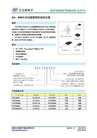
svf2n65f svf2n65n svf2n65mj svf2n65d.pdf
SVF2N65F/N/MJ/D 2A 650V N SVF2N65F/N/MJ/D N MOS F-CellTM VDMOS
svf2n65f.pdf
SVF2N65F_Datasheet 2A, 650V N-CHANNEL MOSFET GENERAL DESCRIPTION SVF2N65F is an N-channel enhancement mode power MOS field effect transistor which is produced using Silan proprietary F-CellTM structure VDMOS technology. The improved planar stripe cell and the improved guarding ring terminal have been especially tailored to minimize on-state resistance, provide superior switching
mdis2n65bth.pdf
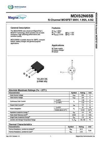
MDIS2N65B N-Channel MOSFET 650V, 1.95A, 4.5 General Description Features The MDIS2N65B uses advanced MagnaChip s V = 650V DS MOSFET technology, which provides low on-state I = 1.95A @V = 10V D GS resistance, high switching performance and RDS(ON) 4.5 @VGS = 10V excellent quality. MDIS2N65B is suitable device for SMPS, compact ballast, battery charge
ms12n65.pdf
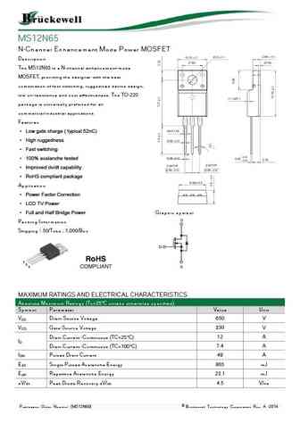
MS12N65 N-Channel Enhancement Mode Power MOSFET Description The MS12N65 is a N-channel enhancement-mode MOSFET, providing the designer with the best combination of fast switching, ruggedized device design, low on-resistance and cost effectiveness. The TO-220 package is universally preferred for all commercial-industrial applications Features Low gate charge ( typical 52n
msf12n65.pdf
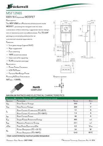
MSF12N65 650V N-Channel MOSFET Description The MSF12N65 is a N-channel enhancement-mode MOSFET , providing the designer with the best combination of fast switching, ruggedized device design, low on-resistance and cost effectiveness. The TO-220F package is universally preferred for all commercial-industrial applications Features Low gate charge ( typical 52nC) High
ru12n65p.pdf
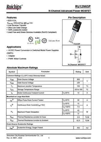
RU12N65P N-Channel Advanced Power MOSFET Features Pin Description 650V/12A, RDS (ON) =650m (Typ.)@VGS=10V Low Reverse Transfer Ultra Low Gate Charge 100% avalanche tested Lead Free and Green Devices Available (RoHS Compliant) Lead Free and Green Devices Available (RoHS Compliant) GD S TO220F D D D D D Applications D pp D AC/DC Power Conversion
ru2n65p.pdf
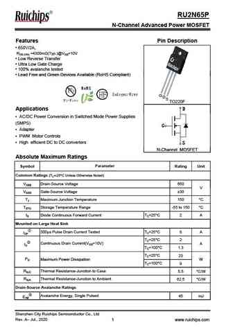
RU2N65P N-Channel Advanced Power MOSFET Features Pin Description 650V/2A, RDS (ON) =4300m (Typ.)@VGS=10V Low Reverse Transfer Ultra Low Gate Charge 100% avalanche tested Lead Free and Green Devices Available (RoHS Compliant) Lead Free and Green Devices Available (RoHS Compliant) GD S TO220F D D D D D Applications D pp D AC/DC Power Conversion i
wfp12n65.pdf
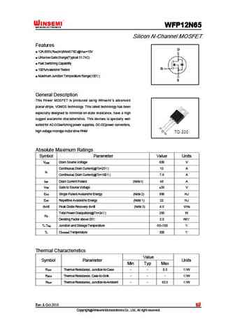
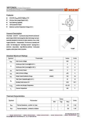
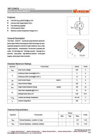
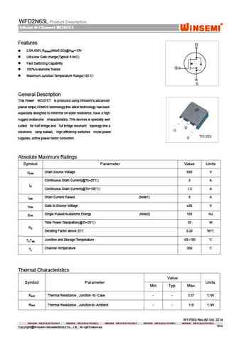
WFP12N65 WFP12N65 WFP12N65 WFP12N65 Silicon N-Channel MOSFET Features 12A,650V,RDS(on)(Max0.78 )@VGS=10V Ultra-low Gate Charge(Typical 51.7nC) Fast Switching Capability 100%Avalanche Tested Maximum Junction Temperature Range(150 ) General Description This Po wer MOS FE T is pro du ced usi ng Win se mi s adva nce d planar stripe, VDMOS technology. This late
wff2n65l.pdf
WFF2N65L Product Description Silicon N-Channel MOSFET Silicon N-Channel MOSFET Silicon N-Channel MOSFET Silicon N-Channel MOSFET Features D 2.0A,650V,R (Max5.0 )@V =10V DS(on) GS Ultra-low Gate charge(Typical 8.6nC) Fast Switching Capability G 100%Avalanche Tested Maximum Junction Temperature Range(150 ) S General Description This Power MOSFET is produced
wff2n65.pdf
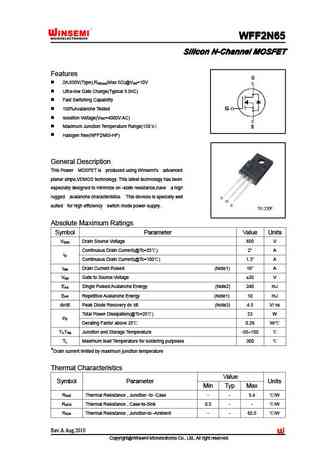
WFF2N65 WFF2N65 WFF2N65 WFF2N65 Silicon N-Channel MOSFET Silicon N-Channel MOSFET Silicon N-Channel MOSFET Silicon N-Channel MOSFET Features 2A,650V(Type),R (Max 5 )@V =10V DS(on) GS Ultra-low Gate Charge(Typical 9.0nC) Fast Switching Capability 100%Avalanche Tested Isolation Voltage(V =4000V AC) ISO Maximum Junction Temperature Range(150 ) Halog
wfu2n65l.pdf
WFU2N65L Product Description Silicon N-Channel MOSFET Silicon N-Channel MOSFET Silicon N-Channel MOSFET Silicon N-Channel MOSFET Features D 2.0A,650V,R (Max5.0 )@V =10V DS(on) GS Ultra-low Gate charge(Typical 8.6nC) Fast Switching Capability G 100%Avalanche Tested Maximum Junction Temperature Range(150 ) S General Description This Power MOSFET is produced
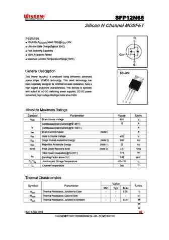
sfp12n65.pdf
SFP12N65 SFP12N65 SFP12N65 SFP12N65 Silicon N-Channel MOSFET Silicon N-Channel MOSFET Silicon N-Channel MOSFET Silicon N-Channel MOSFET Features 12A,650V,RDS(on)(Max0.78 )@VGS=10V Ultra-low Gate Charge(Typical 30nC) Fast Switching Capability 100% Avalanche Tested Maximum Junction Temperature Range(150 ) General Description This Power MOSFET is produced usin
wfd2n65l.pdf
WFD2N65L Product Description Silicon N-Channel MOSFET Silicon N-Channel MOSFET Silicon N-Channel MOSFET Silicon N-Channel MOSFET Features D 2.0A,650V,R (Max5.0 )@V =10V DS(on) GS Ultra-low Gate charge(Typical 8.6nC) Fast Switching Capability G 100%Avalanche Tested Maximum Junction Temperature Range(150 ) S General Description This Power MOSFET is produced
wfp12n65s.pdf
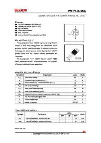
WFP12N65S Super-junction N-Channel Power MOSFET Features 12A,650V,R (Max0.30 )@V =10V DS(on) GS Ultra-low Gate charge(Typical 84.4nC) High EAS energy 100%Avalanche Tested RoHS Compliant Maximum Junction Temperature Range(150 ) General Description This Super-junction Power MOSFET is produced using Winsemi's employs a deep trench filling process t
wff12n65.pdf
WFF12N65 WFF12N65 WFF12N65 WFF12N65 Silicon N-Channel MOSFET Features 12A,650V,RDS(on)(Max0.78 )@VGS=10V Ultra-low Gate Charge(Typical 51.7nC) Fast Switching Capability 100%Avalanche Tested Maximum Junction Temperature Range(150 ) General Description This Power MOSFET is produced using Winsemi s advanced planar stripe, VDMOS technology. This latest technol
wff2n65b.pdf
WFF2N65B WFF2N65B WFF2N65B WFF2N65B Silicon N-Channel MOSFET Silicon N-Channel MOSFET Silicon N-Channel MOSFET Silicon N-Channel MOSFET Features 2A,650V(Type),R (Max 5 )@V =10V DS(on) GS Ultra-low Gate Charge(Typical 9.0nC) Fast Switching Capability 100%Avalanche Tested Isolation Voltage(V =4000V AC) ISO Maximum Junction Temperature Range(150 ) Gener
bl12n65-p bl12n65-a.pdf
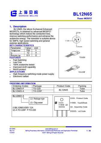
BL12N65 Power MOSFET Power MOSFET Power MOSFET Power MOSFET 1 Description BL12N65, the silicon N-channel Enhanced MOSFETs, is obtained by advanced MOSFET technology which reduce the conduction loss, improve switching performance and enhance the avalanche energy. The transistor is suitable device for SMPS, high speed switching and general purpose application
bl12n65a-p bl12n65a-a.pdf
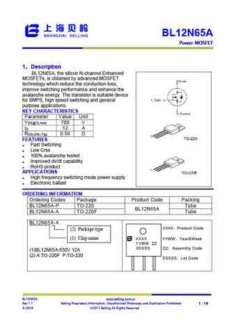
BL12N65A Power MOSFET Power MOSFET Power MOSFET Power MOSFET 1 Description BL12N65A, the silicon N-channel Enhanced MOSFETs, is obtained by advanced MOSFET technology which reduce the conduction loss, improve switching performance and enhance the avalanche energy. The transistor is suitable device for SMPS, high speed switching and general purpose applicati
fhf2n65a fhp2n65a fhu2n65a fhd2n65a.pdf
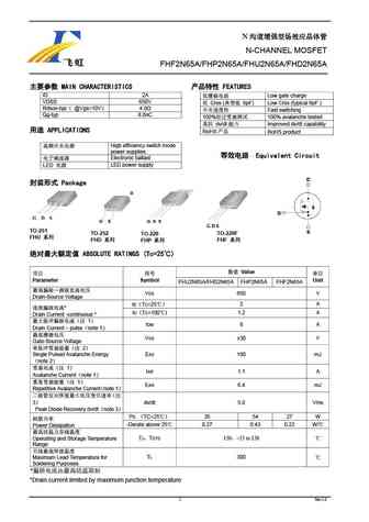
N N-CHANNEL MOSFET FHF2N65A/FHP2N65A/FHU2N65A/FHD2N65A MAIN CHARACTERISTICS FEATURES ID 2A Low gate charge VDSS 650V Crss ( 6pF) Low Crss (typical 6pF ) Rdson-typ @Vgs=10V 4.0 Fast switching Qg-typ 8.0nC 100% 100% avalanche tested dv/
fhp2n65d fhf2n65d fhu2n65d fhd2n65d.pdf
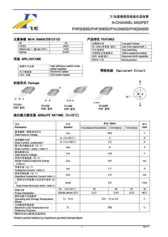
N N-CHANNEL MOSFET FHP2N65D/FHF2N65D/FHU2N65D/FHD2N65D MAIN CHARACTERISTICS FEATURES ID 2A Low gate charge VDSS 650V Crss ( 6pF) Low Crss (typical 6pF ) Rdson-typ @Vgs=10V 4.0 Fast switching Qg-typ 8.0nC 100% 100% avalanche tested dv/
fhp12n65c fhf12n65c.pdf
N N-CHANNEL MOSFET FHP12N65C/ FHF12N65C MAIN CHARACTERISTICS FEATURES Low gate charge ID 12A Crss ( 18pF) Low Crss (typical 18pF ) VDSS 650V Fast switching Rdson-typ 0.63 @Vgs=10V 100% 100% avalanche tested Qg-typ 52nC dv/dt I
2n6517m 3cg6517m.pdf
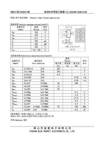
2N6517M(3CG6517M) NPN /SILICON NPN TRANSISTOR /Purpose High voltage application. /Absolute maximum ratings(Ta=25 ) Symbol Rating Unit V 350 V CBO V 350 V CEO V 6.0 V EBO I 500 mA C P 300 mW C T 150 j T -55 150 stg /Electrical characteristics(T
hy12n65t.pdf
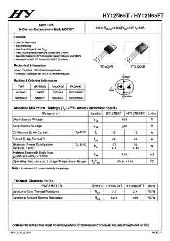
HY12N65T / HY12N65FT 650V / 12A 650V, RDS(ON)=0.8 @VGS=10V, ID=6.0A N-Channel Enhancement Mode MOSFET Features Low ON Resistance Fast Switching Low Gate Charge & Low CRSS Fully Characterized Avalanche Voltage and Current Specially Desigened for AC Adapter, Battery Charger and SMPS 1 1 2 2 In compliance with EU RoHs 2002/95/EC Directives G G 3 3 D D S S
hy2n65d.pdf
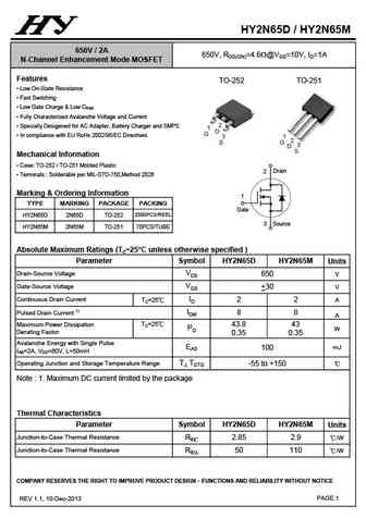
SINGLE FIG.SINGLE CURVE FIG. 2 NON- T1 FORWARD CURRENT AMBIENT 1 2MAXIMUM5 10 1 25 50 PHASE HALF WAVE 60Hz ( ) 150 175 0.00 0.2 0.4 0.6 4 TEMPERATURE DERATING 100 75 10 20 100 125 HY2N65D / HY2N65M 650V / 2A 650V, RDS(ON)=4.6W@VGS=10V, ID=1A N-Channel Enhancement Mode MOSFET Features TO-252 TO-251 Low On-State Resistance Fast Switching Low Gate Cha
hy2n65t.pdf
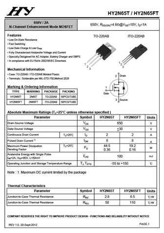
HY2N65T / HY2N65FT 650V / 2A 650V, RDS(ON)=4.6W@VGS=10V, ID=1A N-Channel Enhancement Mode MOSFET Features TO-220AB ITO-220AB Low On-State Resistance Fast Switching Low Gate Charge & Low CRSS Fully Characterized Avalanche Voltage and Current Specially Desigened for AC Adapter, Battery Charger and SMPS In compliance with EU RoHs 2002/95/EC Directives 1 1
jfpc12n65c.pdf
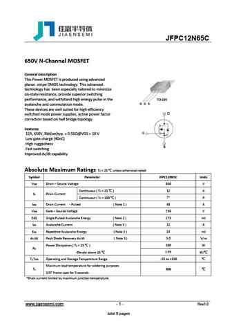
JFPC12N65C 650V N-Channel MOSFET General Description This Power MOSFET is produced using advanced planar stripe DMOS technology. This advanced technology has been especially tailored to minimize on-state resistance, provide superior switching performance, and withstand high energy pulse in the avalanche and commutation mode. These devices are well suited for high efficiency
jfpc12n65d.pdf
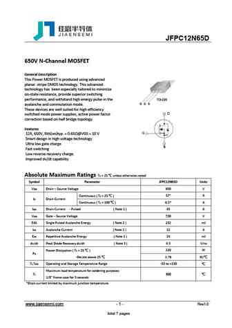
JFPC12N65D 650V N-Channel MOSFET General Description This Power MOSFET is produced using advanced planar stripe DMOS technology. This advanced technology has been especially tailored to minimize on-state resistance, provide superior switching performance, and withstand high energy pulse in the avalanche and commutation mode. These devices are well suited for high efficiency
kia12n65h.pdf
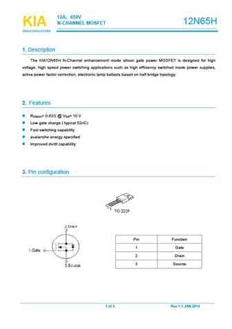
12A 650V 12N65H N-CHANNELMOSFET KIA KIA KIA SEMICONDUCTORS SEMICONDUCTORS SEMICONDUCTORS 1.Description The KIA12N65H N-Channel enhancement mode silicon gate power MOSFET is designed for high voltage, high speed power switching applications such as high efficiency switched mode power supplies, active power factor correction, electronic lamp ballasts based on half bridge topology.
slf12n65sv.pdf
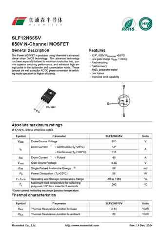
SLF12N65SV 650V N-Channel MOSFET General Description Features This Power MOSFET is produced using Msemitek s advanced 12A*, 650V, RDS(on),typ =0.67 planar stripe DMOS technology. This advanced technology Low gate charge (Qg,typ = 33nC) has been especially tailored to minimize conduction loss, pro- Fast switching vide superior switching performance, and withstand high en-
sld2n65uz slu2n65uz.pdf
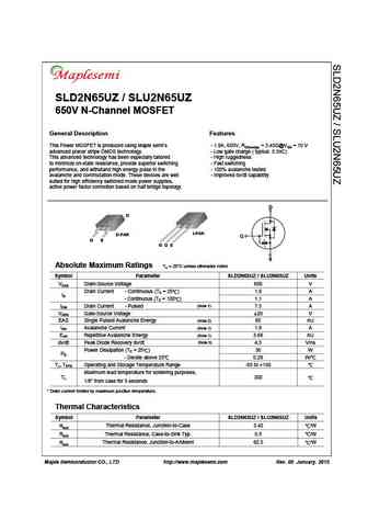
SLD2N65UZ / SLU2N65UZ 650V N-Channel MOSFET General Description Features This Power MOSFET is produced using Maple semi s - 1.9A, 650V, RDS(on)typ = 3.45 @VGS = 10 V advanced planar stripe DMOS technology. - Low gate charge ( typical 5.5nC) This advanced technology has been especially tailored - High ruggedness to minimize on-state resistance, provide superior switching - Fast switchin
slp12n65c slf12n65c.pdf
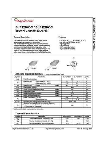
SLP12N65C / SLF12N65C 650V N-Channel MOSFET General Description Features This Power MOSFET is produced using Maple semi s - 12A, 650V, RDS(on) typ. = 0.6 @VGS = 10 V advanced planar stripe DMOS technology. - Low gate charge ( typical 47nC) This advanced technology has been especially tailored - High ruggedness to minimize on-state resistance, provide superior switching - Fast switching
slp2n65uz slf2n65uz.pdf

SLP2N65UZ / SLF2N65UZ 650V N-Channel MOSFET General Description Features This Power MOSFET is produced using Maple semi s - 2.0A, 650V, RDS(on) typ. = 4.3 @VGS = 10 V advanced planar stripe DMOS technology. - Low gate charge ( typical 6.5nC) This advanced technology has been especially tailored - High ruggedness to minimize on-state resistance, provide superior switching - Fast switchi
pta22n65.pdf
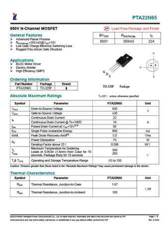
PTA22N65 650V N-Channel MOSFET General Features BVDSS RDS(ON),typ. ID Advanced Planar Process 650V 350m 22A RDS(ON),typ.=350 m @VGS=10V Low Gate Charge Minimize Switching Loss Rugged Poly silicon Gate Structure Applications BLDC Motor Driver Electric Welder High Efficiency SMPS G D S Ordering Information Part Number Package Brand TO-220F Package P
ptp12n65 pta12n65.pdf
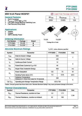
PTP12N65 PTA12N65 650V N-ch Planar MOSFET General Features BVDSS RDS(ON),typ. ID RoHS Compliant 650V 0.60 12A RDS(ON),typ.=0.60 @VGS=10V Low Gate Charge Minimize Switching Loss Fast Recovery Body Diode Applications Adaptor Charger G D S G D SMPS Standby Power S Ordering Information TO-220 TO-220F Part Number Package Brand
swf2n65d.pdf
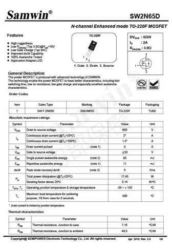
SW2N65D N-channel Enhanced mode TO-220F MOSFET Features TO-220F BVDSS 650V ID 2A High ruggedness Low RDS(ON) (Typ 3.9 )@VGS=10V RDS(ON) 3.9 Low Gate Charge (Typ 9nC) Improved dv/dt Capability 2 100% Avalanche Tested 1 2 Application Adapter,LED 3 1 1. Gate 2. Drain 3. Source 3 General Description This power MOSFET is produc
sw2n65b.pdf
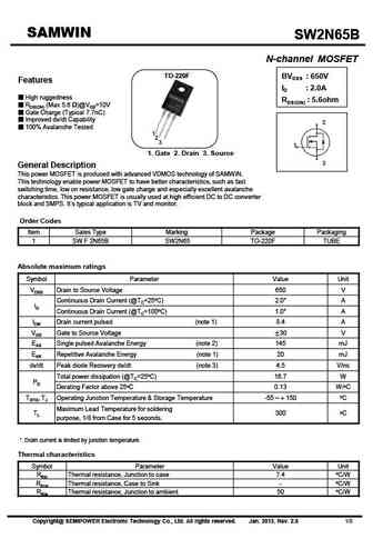
SAMWIN SW2N65B SW2N65B N-channel MOSFET TO-220F BVDSS 650V Features ID 2.0A High ruggedness RDS(ON) 5.6ohm RDS(ON) (Max 5.6 )@VGS=10V Gate Charge (Typical 7.7nC) Improved dv/dt Capability 2 100% Avalanche Tested 1 2 3 1 1. Gate 2. Drain 3. Source 3 General Description This power MOSFET is produced with advanced VDMOS technology of SAMWIN. This
swf12n65d swu12n65d swp12n65d swb12n65d.pdf
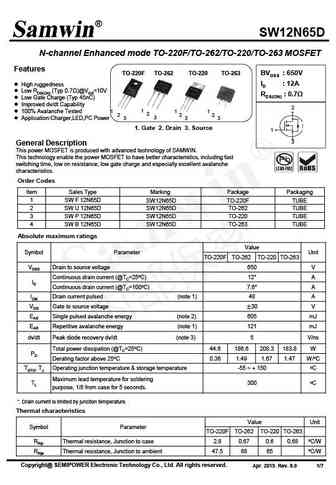
SW12N65D N-channel Enhanced mode TO-220F/TO-262/TO-220/TO-263 MOSFET Features TO-220F TO-262 TO-220 TO-263 BVDSS 650V High ruggedness ID 12A Low RDS(ON) (Typ 0.7 )@VGS=10V RDS(ON) 0.7 Low Gate Charge (Typ 45nC) Improved dv/dt Capability 2 1 100% Avalanche Tested 1 1 1 2 2 2 2 3 Application Charger,LED,PC Power 3 3 3 1. Gate 2.
swmn12n65da.pdf
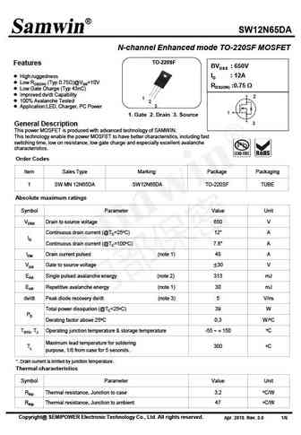
SW12N65DA N-channel Enhanced mode TO-220SF MOSFET TO-220SF Features BVDSS 650V ID 12A High ruggedness Low RDS(ON) (Typ 0.75 )@VGS=10V RDS(ON) 0.75 Low Gate Charge (Typ 43nC) Improved dv/dt Capability 2 1 100% Avalanche Tested 2 3 Application LED, Charger, PC Power 1 1. Gate 2. Drain 3. Source 3 General Description Th
sw2n65.pdf
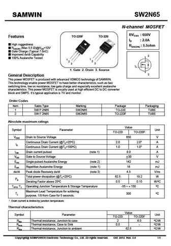
SW2N65 SAMWIN N-channel MOSFET BVDSS 650V TO-220F TO-220 Features ID 2.0A High ruggedness RDS(ON) 5.5ohm RDS(ON) (Max 5.5 )@VGS=10V Gate Charge (Typical 7.8nC) Improved dv/dt Capability 2 100% Avalanche Tested 1 1 2 2 3 3 1 1. Gate 2. Drain 3. Source 3 General Description This power MOSFET is produced with advanced VDMOS technology of SAMWIN.
swmn12n65d swy12n65d.pdf
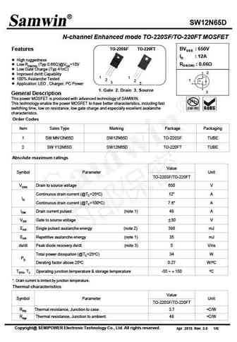
SW12N65D N-channel Enhanced mode TO-220SF/TO-220FT MOSFET TO-220SF TO-220FT BVDSS 650V Features ID 12A High ruggedness RDS(ON) 0.66 Low RDS(ON) (Typ 0.66 )@VGS=10V Low Gate Charge (Typ 41nC) 2 Improved dv/dt Capability 1 1 100% Avalanche Tested 2 1 2 3 3 Application LED , Charger, PC Power 1. Gate 2. Drain 3. Source
sw12n65d swf12n65d swu12n65d swp12n65d swb12n65d.pdf

SW12N65D N-channel Enhanced mode TO-220F/TO-262/TO-220/TO-263 MOSFET Features TO-262 TO-220F TO-220 TO-263 BVDSS 650V High ruggedness ID 12A Low RDS(ON) (Typ 0.7 )@VGS=10V RDS(ON) 0.7 Low Gate Charge (Typ 45nC) Improved dv/dt Capability 2 1 100% Avalanche Tested 1 1 1 2 2 2 2 3 Application Charge,LED,PC Power 3 3 3 1. Gate 2
swt22n65d.pdf
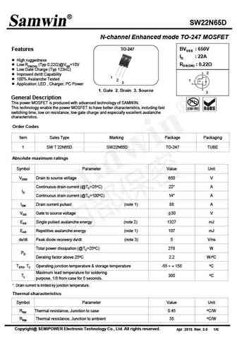
SW22N65D N-channel Enhanced mode TO-247 MOSFET TO-247 BVDSS 650V Features ID 22A High ruggedness RDS(ON) 0.22 Low RDS(ON) (Typ 0.22 )@VGS=10V Low Gate Charge (Typ 123nC) 2 Improved dv/dt Capability 1 100% Avalanche Tested 2 1 3 Application LED , Charger, PC Power 1. Gate 2. Drain 3. Source 3 General Description This p
swf2n65db.pdf
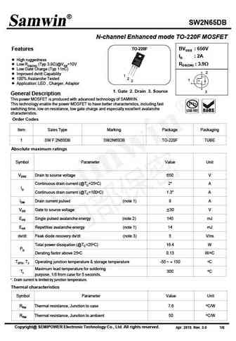
SW2N65DB N-channel Enhanced mode TO-220F MOSFET TO-220F BVDSS 650V Features ID 2A High ruggedness RDS(ON) 3.9 Low RDS(ON) (Typ 3.9 )@VGS=10V Low Gate Charge (Typ 11nC) 2 Improved dv/dt Capability 1 100% Avalanche Tested 2 1 3 Application LED , Charger, Adaptor 1. Gate 2. Drain 3. Source 3 General Description This power
swn2n65k swd2n65k.pdf
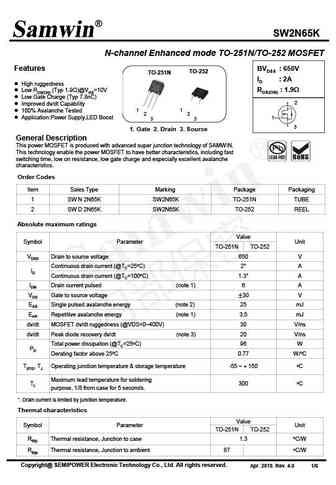
SW2N65K N-channel Enhanced mode TO-251N/TO-252 MOSFET Features BVDSS 650V TO-252 TO-251N ID 2A High ruggedness Low RDS(ON) (Typ 1.9 )@VGS=10V RDS(ON) 1.9 Low Gate Charge (Typ 7.8nC) 2 Improved dv/dt Capability 100% Avalanche Tested 1 1 2 2 Application Power Supply,LED Boost 1 3 3 3 1. Gate 2. Drain 3. Source General Descrip
srm12n65.pdf
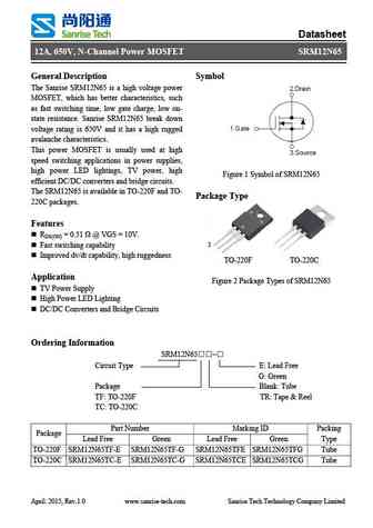
Datasheet 12A, 650V, N-Channel Power MOSFET SRM12N65 General Description Symbol The Sanrise SRM12N65 is a high voltage power MOSFET, which has better characteristics, such as fast switching time, low gate charge, low on- state resistance. Sanrise SRM12N65 break down voltage rating is 650V and it has a high rugged avalanche characteristics. This power MOSFET is usually used at hi
hfp12n65s.pdf
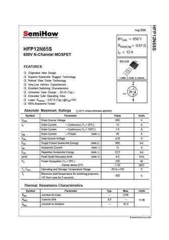
Aug 2009 BVDSS = 650 V RDS(on) typ = 0.67 HFP12N65S ID = 12 A 650V N-Channel MOSFET TO-220 FEATURES Originative New Design 1 2 3 Superior Avalanche Rugged Technology 1.Gate 2. Drain 3. Source Robust Gate Oxide Technology Very Low Intrinsic Capacitances Excellent Switching Characteristics Unrivalled Gate Charge 38 nC (Typ.) Unrivalled Gate Charge 38 nC (Typ ) Ext
hfp2n65u.pdf
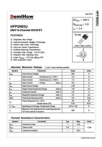
Nov 2013 BVDSS = 650 V RDS(on) typ = 5 HFP2N65U ID = 2 A 650V N-Channel MOSFET TO-220 FEATURES Originative New Design Superior Avalanche Rugged Technology 1 2 3 Robust Gate Oxide Technology 1.Gate 2. Drain 3. Source Very Low Intrinsic Capacitances Excellent Switching Characteristics Unrivalled Gate Charge 5.5 nC (Typ.) Extended Safe Operating Area Lower R
hfp2n65s.pdf
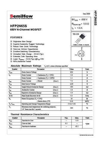
Sep 2009 BVDSS = 650 V RDS(on) typ HFP2N65S ID = 1.8 A 650V N-Channel MOSFET TO-220 FEATURES Originative New Design 1 2 3 Superior Avalanche Rugged Technology 1.Gate 2. Drain 3. Source Robust Gate Oxide Technology Very Low Intrinsic Capacitances Excellent Switching Characteristics Unrivalled Gate Charge 6.0 nC (Typ.) Extended Safe Operating Area Lower RDS(O
hfs2n65u.pdf
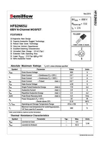
Nov 2013 BVDSS = 650 V RDS(on) typ = 5 HFS2N65U ID = 2 A 650V N-Channel MOSFET TO-220F FEATURES Originative New Design Superior Avalanche Rugged Technology 1 2 3 Robust Gate Oxide Technology 1.Gate 2. Drain 3. Source Very Low Intrinsic Capacitances Excellent Switching Characteristics Unrivalled Gate Charge 5.5 nC (Typ.) Extended Safe Operating Area Lower
hfs12n65sa.pdf
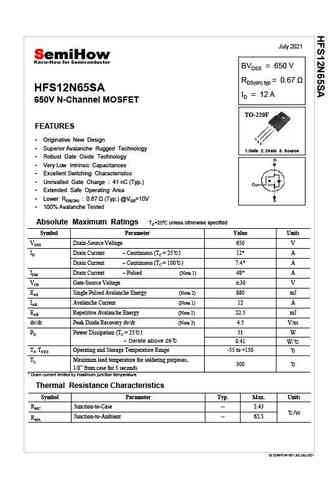
July 2021 BVDSS = 650 V RDS(on) typ = 0.67 HFS12N65SA ID = 12 A 650V N-Channel MOSFET TO-220F FEATURES 1 Originative New Design 2 3 Superior Avalanche Rugged Technology 1.Gate 2. Drain 3. Source Robust Gate Oxide Technology Very Low Intrinsic Capacitances Excellent Switching Characteristics Unrivalled Gate Charge 41 nC (Typ.) Extended Safe Ope
hfs12n65s.pdf
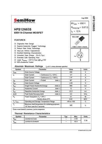
Aug 2009 BVDSS = 650 V RDS(on) typ = 0.67 HFS12N65S ID = 12 A 650V N-Channel MOSFET TO-220F FEATURES 1 Originative New Design 2 3 Superior Avalanche Rugged Technology 1.Gate 2. Drain 3. Source Robust Gate Oxide Technology Very Low Intrinsic Capacitances Excellent Switching Characteristics Unrivalled Gate Charge 38 nC (Typ.) Unrivalled Gate Charge 38 nC (Typ ) E
hfd2n65s.pdf
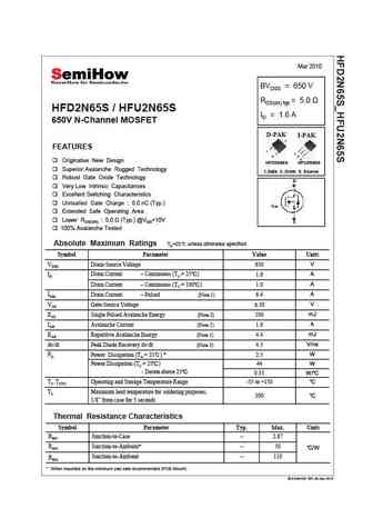
Mar 2010 BVDSS = 650 V RDS(on) typ = 5.0 HFD2N65S / HFU2N65S ID = 1.6 A 650V N-Channel MOSFET D-PAK I-PAK 2 2 FEATURES 1 1 3 2 3 Originative New Design HFD2N65S HFU2N65S Superior Avalanche Rugged Technology 1.Gate 2. Drain 3. Source Robust Gate Oxide Technology Very Low Intrinsic Capacitances Excellent Switching Characteristics Unrivalled Gate Charge 6.0 nC (Typ.
hfp12n65u.pdf
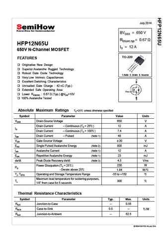
July 2014 BVDSS = 650 V RDS(on) typ = 0.67 HFP12N65U ID = 12 A 650V N-Channel MOSFET TO-220 FEATURES Originative New Design Superior Avalanche Rugged Technology 1 2 3 Robust Gate Oxide Technology 1.Gate 2. Drain 3. Source Very Low Intrinsic Capacitances Excellent Switching Characteristics Unrivalled Gate Charge 42 nC (Typ.) Extended Safe Operating Area Lo
hfd2n65u.pdf
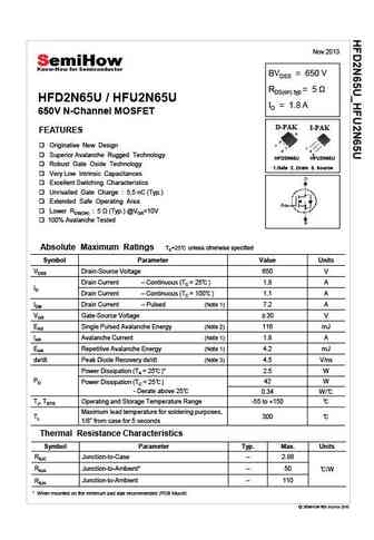
Nov 2013 BVDSS = 650 V RDS(on) typ = 5 HFD2N65U / HFU2N65U ID = 1.8 A 650V N-Channel MOSFET D-PAK I-PAK FEATURES 2 1 Originative New Design 1 3 2 3 Superior Avalanche Rugged Technology HFD2N65U HFU2N65U Robust Gate Oxide Technology 1.Gate 2. Drain 3. Source Very Low Intrinsic Capacitances Excellent Switching Characteristics Unrivalled Gate Charge 5.5 nC (Ty
hfs12n65js.pdf
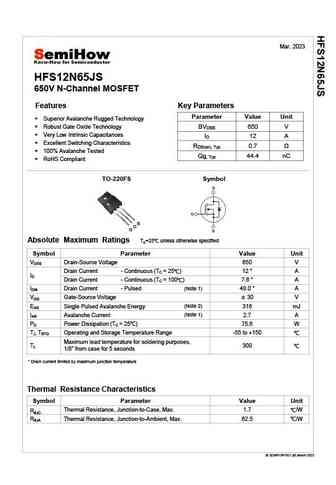
Mar. 2023 HFS12N65JS 650V N-Channel MOSFET Features Key Parameters Parameter Value Unit Superior Avalanche Rugged Technology BVDSS 650 V Robust Gate Oxide Technology Very Low Intrinsic Capacitances ID 12 A Excellent Switching Characteristics RDS(on), Typ 0.7 100% Avalanche Tested Qg, Typ 44.4 nC RoHS Compliant TO-220FS Symbol S D G Absolute Maximum
hfs2n65s.pdf
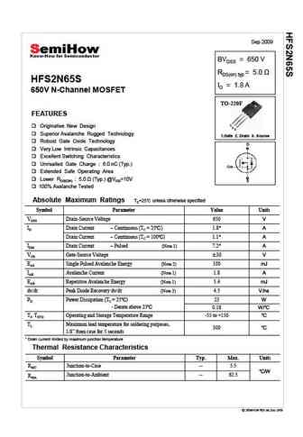
Sep 2009 BVDSS = 650 V RDS(on) typ HFS2N65S ID = 1.8 A 650V N-Channel MOSFET TO-220F FEATURES 1 Originative New Design 2 3 Superior Avalanche Rugged Technology 1.Gate 2. Drain 3. Source Robust Gate Oxide Technology Very Low Intrinsic Capacitances Excellent Switching Characteristics Unrivalled Gate Charge 6.0 nC (Typ.) Extended Safe Operating Area Lower RDS
hfs12n65u.pdf
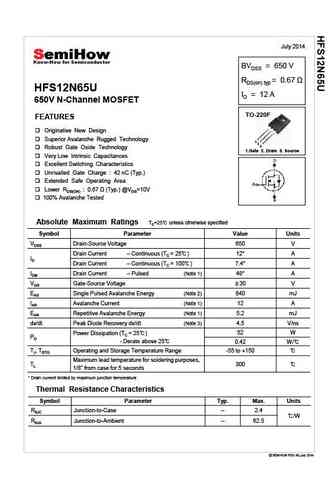
July 2014 BVDSS = 650 V RDS(on) typ = 0.67 HFS12N65U ID = 12 A 650V N-Channel MOSFET TO-220F FEATURES Originative New Design Superior Avalanche Rugged Technology 1 2 3 Robust Gate Oxide Technology 1.Gate 2. Drain 3. Source Very Low Intrinsic Capacitances Excellent Switching Characteristics Unrivalled Gate Charge 42 nC (Typ.) Extended Safe Operating Area Lo
sl2n65f.pdf
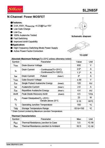
SL2N65F N-Channel Power MOSFET Features 2.0A, 650V, R =4.2 @V =10V DS(on)(Typ) GS Low Gate Charge Low C rss 100% Avalanche Tested Schematic diagram Fast Switching Improved dv/dt Capability Application High Frequency Switching Mode Power Supply Active Power Factor Correction TO-220F Absolute Maximum Ratings(Tc=25 C unless otherwise
tmp2n65az tmpf2n65az.pdf
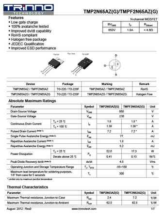
TMP2N65AZ(G)/TMPF2N65AZ(G) Features N-channel MOSFET Low gate charge BVDSS ID RDS(on) 100% avalanche tested 650V 1.8A
tmd2n65az tmu2n65az.pdf
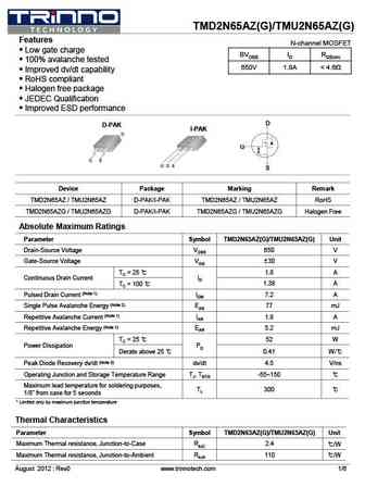
TMD2N65AZ(G)/TMU2N65AZ(G) Features N-channel MOSFET Low gate charge BVDSS ID RDS(on) 100% avalanche tested 650V 1.8A
tsp12n65m tsf12n65m.pdf
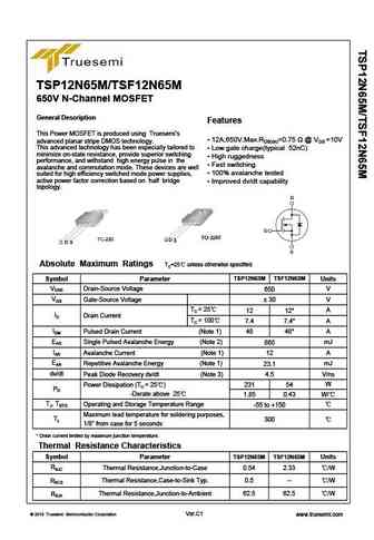
TSP12N65M/TSF12N65M 650V N-Channel MOSFET General Description Features This Power MOSFET is produced using Truesemi s 12A,650V,Max.RDS(on)=0.75 @ VGS =10V advanced planar stripe DMOS technology. This advanced technology has been especially tailored to Low gate charge(typical 52nC) minimize on-state resistance, provide superior switching High ruggedness performance, a
qm12n65f.pdf
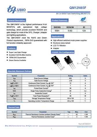
QM12N65F 1 2011-03-03 - 1 - N-Ch 650V Fast Switching MOSFETs General Description Product Summery The QM12N65F is the highest performance N-ch MOSFETs with specialized high voltage BVDSS RDSON ID technology, which provide excellent RDSON and 650V 0.8 12A gate charge for most of the SPS, Charger ,Adapter and lighting applications . Applications The QM12N65F me
qm12n65p.pdf
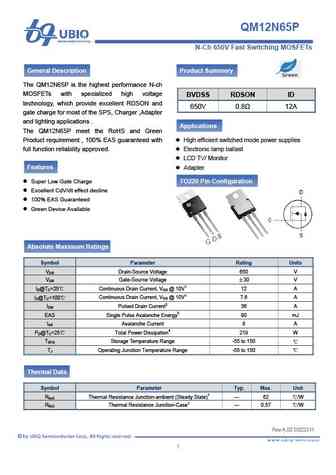
QM12N65P 1 2011-03-03 - 1 - N-Ch 650V Fast Switching MOSFETs General Description Product Summery The QM12N65P is the highest performance N-ch MOSFETs with specialized high voltage BVDSS RDSON ID technology, which provide excellent RDSON and 650V 0.8 12A gate charge for most of the SPS, Charger ,Adapter and lighting applications . Applications The QM12N65P me
qm12n65b.pdf
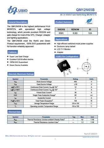
QM12N65B 1 2011-03-03 - 1 - N-Ch 650V Fast Switching MOSFETs General Description Product Summery The QM12N65B is the highest performance N-ch MOSFETs with specialized high voltage BVDSS RDSON ID technology, which provide excellent RDSON and 650V 0.8 12A gate charge for most of the SPS, Charger ,Adapter and lighting applications . Applications The QM12N65B m
qm02n65u.pdf
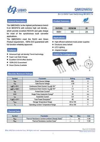
QM02N65U 1 2010-04-27 - 1 - N-Ch 650V Fast Switching MOSFETs General Description Product Summery The QM02N65U is the highest performance trench N-ch MOSFETs with extreme high cell density , BVDSS RDSON ID which provide excellent RDSON and gate charge 650V 8 2A for most of the synchronous buck converter applications . Applications The QM02N65U meet the RoHS
qm02n65d.pdf
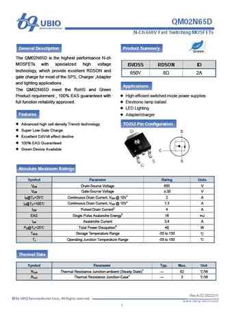
QM02N65D 1 2011-03-03 - 1 - N-Ch 650V Fast Switching MOSFETs General Description Product Summery The QM02N65D is the highest performance N-ch MOSFETs with specialized high voltage BVDSS RDSON ID technology, which provide excellent RDSON and 650V 8 2A gate charge for most of the SPS, Charger ,Adapter and lighting applications . Applications The QM02N65D meet
wml12n65d1b wmk12n65d1b.pdf
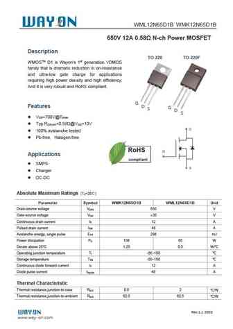
WML12N65D1B WMK12N65D1B 650V 12A 0.58 N-ch Power MOSFET Description TO-220 TO-220F WMOSTM D1 is Wayon s 1st generation VDMOS family that is dramatic reduction in on-resistance and ultra-low gate charge for applications requiring high power density and high efficiency. And it is very robust and RoHS compliant. G Features D G S D S V =700V@T DS jmax Typ.R =0.58 @V =1
wml12n65d1 wmk12n65d1.pdf

WML12N65D1 WMK12N65D1 650V 12A 0.58 N-ch Power MOSFET Description TO-220 TO-220F WMOSTM D1 is Wayon s 1st generation VDMOS family that is dramatic reduction in on-resistance and ultra-low gate charge for applications requiring high power density and high efficiency. And it is very robust and RoHS compliant. G Features D G S D S V =700V@T DS jmax Typ.R =0.58 @V =10V
cs12n65fa9h.pdf

Silicon N-Channel Power MOSFET R CS12N65F A9H VDSS 650 V General Description ID 12 A CS12N65F A9H, the silicon N-channel Enhanced PD (TC=25 ) 55 W VDMOSFETs, is obtained by the self-aligned planar RDS(ON)Typ 0.54 Technology which reduce the conduction loss, improve switching performance and enhance the avalanche energy. The transistor can be used in various
cs2n65a4.pdf
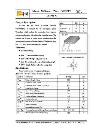
Silicon N-Channel Power MOSFET R CS2N65 A4 General Description VDSS 650 V CS2N65 A4, the silicon N-channel Enhanced ID 2 A PD (TC=25 ) 35 W VDMOSFETs, is obtained by the self-aligned planar RDS(ON)Typ 3.9 Technology which reduce the conduction loss, improve switching performance and enhance the avalanche energy. The transistor can be used in various power s
cs2n65a3hy.pdf
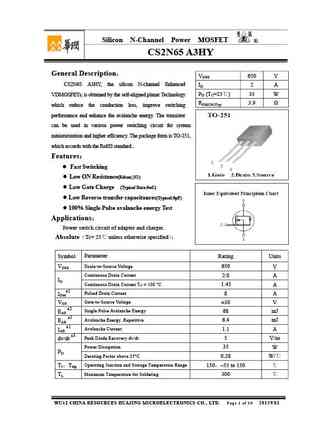
Silicon N-Channel Power MOSFET R CS2N65 A3HY General Description VDSS 650 V CS2N65 A3HY, the silicon N-channel Enhanced ID 2 A PD (TC=25 ) 35 W VDMOSFETs, is obtained by the self-aligned planar Technology RDS(ON)Typ 3.9 which reduce the conduction loss, improve switching performance and enhance the avalanche energy. The transistor can be used in various power
cs12n65a8h.pdf

Silicon N-Channel Power MOSFET R CS12N65 A8H VDSS 650 V General Description ID 12 A CS12N65 A8H, the silicon N-channel Enhanced PD (TC=25 ) 140 W VDMOSFETs, is obtained by the self-aligned planar RDS(ON)Typ 0.54 Technology which reduce the conduction loss, improve switching performance and enhance the avalanche energy. The transistor can be used in various p
cs12n65fa9r.pdf

Silicon N-Channel Power MOSFET R CS12N65F A9R General Description VDSS 650 V CS12N65F A9R, the silicon N-channel Enhanced ID 12 A PD(TC=25 ) 42 W VDMOSFETs, is obtained by the self-aligned planar Technology RDS(ON)Typ 0.66 which reduce the conduction loss, improve switching performance and enhance the avalanche energy. The transistor can be used in various p
cs2n65fa9hy.pdf

Silicon N-Channel Power MOSFET R CS2N65F A9HY General Description VDSS 650 V CS2N65F A9HY, the silicon N-channel Enhanced ID 2.0 A PD (TC=25 ) 27 W VDMOSFETs, is obtained by the self-aligned planar Technology RDS(ON)Typ 4 which reduce the conduction loss, improve switching performance and enhance the avalanche energy. The transistor can be used in various p
cs2n65fa9.pdf
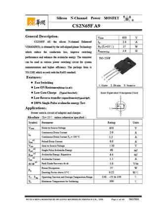
Silicon N-Channel Power MOSFET R CS2N65F A9 General Description VDSS 650 V CS2N65F A9, the silicon N-channel Enhanced ID 2.0 A PD (TC=25 ) 27 W VDMOSFETs, is obtained by the self-aligned planar Technology RDS(ON)Typ 3.9 which reduce the conduction loss, improve switching performance and enhance the avalanche energy. The transistor can be used in various pow
cs2n65a3.pdf

Silicon N-Channel Power MOSFET R CS2N65 A3 General Description VDSS 650 V CS2N65 A3, the silicon N-channel Enhanced ID 2 A PD (TC=25 ) 35 W VDMOSFETs, is obtained by the self-aligned planar Technology RDS(ON)Typ 3.9 which reduce the conduction loss, improve switching performance and enhance the avalanche energy. The transistor can be used in various power swi
cs2n65a4hy.pdf
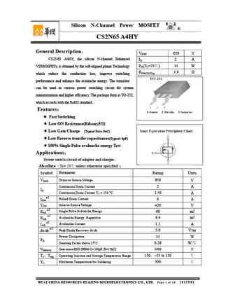
Silicon N-Channel Power MOSFET R CS2N65 A4HY General Description VDSS 650 V CS2N65 A4HY, the silicon N-channel Enhanced ID 2 A PD(TC=25 ) 35 W VDMOSFETs, is obtained by the self-aligned planar Technology RDS(ON)Typ 3.9 which reduce the conduction loss, improve switching performance and enhance the avalanche energy. The transistor can be used in various power
atm2n65tf.pdf
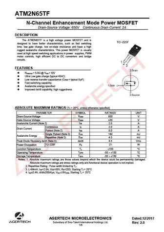
ATM2N65TF N-Channel Enhancement Mode Power MOSFET Drain-Source Voltage 650V Continuous Drain Current 2A DESCRIPTION The ATM2N65TF is a high voltage power MOSFET and is designed to have better characteristics, such as fast switching time, low gate charge, low on-state resistance and have a high rugged avalanche characteristics. This power MOSFET is usually used at high speed sw
atm2n65te.pdf
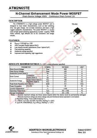
ATM2N65TE N-Channel Enhancement Mode Power MOSFET Drain-Source Voltage 650V Continuous Drain Current 2A DESCRIPTION The ATM2N65TE is a high voltage power MOSFET and is designed to have better characteristics, such as fast switching time, low gate charge, low on-state resistance and have a high rugged avalanche characteristics. This power MOSFET is usually used at high speed sw
atm2n65td.pdf
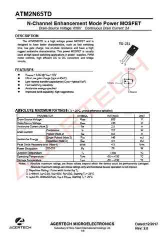
ATM2N65TD N-Channel Enhancement Mode Power MOSFET Drain-Source Voltage 650V Continuous Drain Current 2A DESCRIPTION The ATM2N65TD is a high voltage power MOSFET and is designed to have better characteristics, such as fast switching time, low gate charge, low on-state resistance and have a high rugged avalanche characteristics. This power MOSFET is usually used at high speed sw
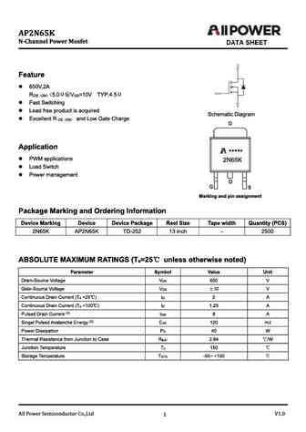
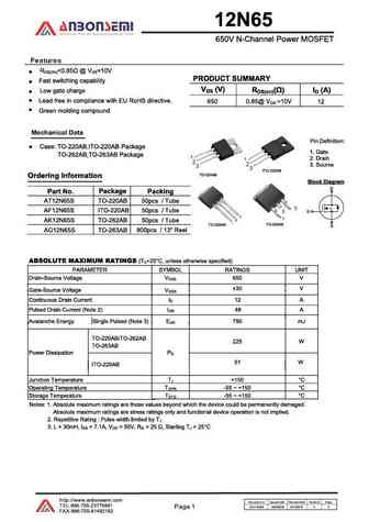
asdm12n65f.pdf
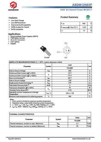
ASDM12N65F 650V N-Channel Power MOSFET Product Summary Features Low Gate Charge Low ON Resistance V DS 650 V Improved dv/dt Capability 100% Avalanche Tested R DS(on),Typ@ VGS=10 V 0.65 RoHS compliant I D 12 A Applications Switching Mode Power Supplies (SMPS) PWM Motor Controls AC to DC Converters LED Lighting Adapter ABSOLUTE MAXIMU
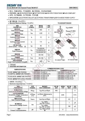
cs12n65f cs12n65p.pdf
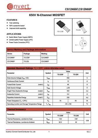
nvert Suzhou Convert Semiconductor Co ., Ltd. CS12N65F,CS12N65P 650V N-Channel MOSFET FEATURES Fast switching 100% avalanche tested Improved dv/dt capability APPLICATIONS Switch Mode Power Supply (SMPS) Uninterruptible Power Supply (UPS) Power Factor Correction (PFC) Device Marking and Package Information Device Package Marking CS12N65F TO-220F CS12N65F CS
cs2n65f cs2n65d cs2n65u.pdf
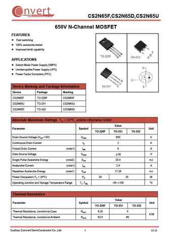
nvert Suzhou Convert Semiconductor Co ., Ltd. CS2N65F,CS2N65D,CS2N65U 650V N-Channel MOSFET FEATURES Fast switching 100% avalanche tested Improved dv/dt capability APPLICATIONS Switch Mode Power Supply (SMPS) Uninterruptible Power Supply (UPS) Power Factor Correction (PFC) Device Marking and Package Information Device Package Marking CS2N65F TO-220F CS2N65F
cs12n65ff.pdf
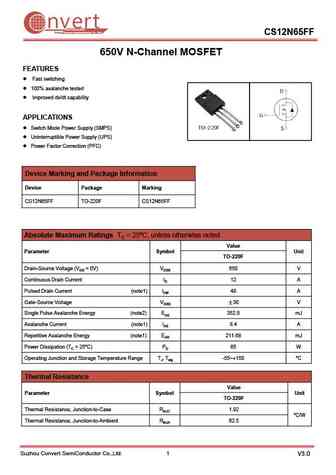
nvert Suzhou Convert Semiconductor Co ., Ltd. CS12N65FF 650V N-Channel MOSFET FEATURES Fast switching 100% avalanche tested Improved dv/dt capability APPLICATIONS Switch Mode Power Supply (SMPS) Uninterruptible Power Supply (UPS) Power Factor Correction (PFC) Device Marking and Package Information Device Package Marking CS12N65FF TO-220F CS12N65FF Absolute
fir12n65fg.pdf
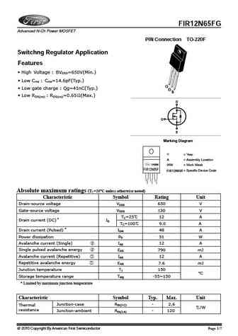
FIR12N65FG Advanced N-Ch Power MOSFET PIN Connection TO-220F Switchng Regulator Application Features High Voltage BVDSS=650V(Min.) Low Crss Crss=14.6pF(Typ.) G Low gate charge Qg=41nC(Typ.) D S Low RDS(on) RDS(on)=0.65 (Max.) D G S Marking Diagram Y = Year A = Assembly Location YAWW WW = Work Week FIR12N65F FIR12N65F = Specific Device C
fir2n65afg.pdf
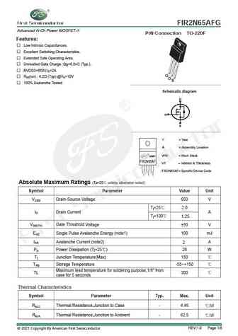
FIR2N65AFG Advanced N-Ch Power MOSFET-X PIN Connection TO-220F Features Low Intrinsic Capacitances. Excellent Switching Characteristics. Extended Safe Operating Area. Unrivalled Gate Charge Qg=6.5nC (Typ.). BVDSS=650V,ID=2A G RDS(on) 4.2 (Typ) @VG=10V DS 100% Avalanche Tested g Schematic dia ram D G S Y = Year A = Assembly Location WW = Wor
fir2n65abpg.pdf
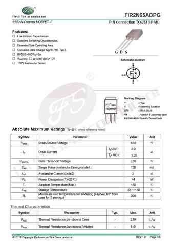
FIR2N65ABPG FIR2N65ABPG 650V N-Channel MOSFET -I PIN Connection TO-251(I-PAK) Features Low Intrinsic Capacitances. Excellent Switching Characteristics. Extended Safe Operating Area. Unrivalled Gate Charge Qg=6.7nC (Typ.). G D S BVDSS=650V,ID=2A RDS(on) 5.0 (Max) @VG=10V g Schematic dia ram 100% Avalanche Tested D G S Marking Diagram Y
smd2n65.pdf
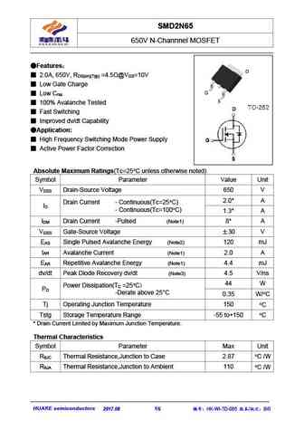
SMD2N65 650V N-Channnel MOSFET Features 2.0A, 650V, R =4.5 @V =10V DS(on)(Typ) GS Low Gate Charge Low C rss 100% Avalanche Tested Fast Switching Improved dv/dt Capability Application High Frequency Switching Mode Power Supply Active Power Factor Correction Absolute Maximum Ratings(Tc=25 C unless otherwise noted) Symbol Parameter Value
smf2n65.pdf

SMF2N65 650V N-Channnel MOSFET Features 2.0A, 650V, R =4.2 @V =10V DS(on)(Typ) GS Low Gate Charge Low C rss 100% Avalanche Tested Fast Switching Improved dv/dt Capability Application High Frequency Switching Mode Power Supply Active Power Factor Correction Absolute Maximum Ratings(Tc=25 C unless otherwise noted) Symbol Parameter Value
smf12n65.pdf
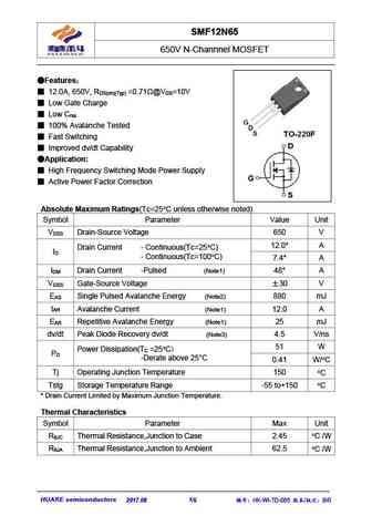
SMF12N65 650V N-Channnel MOSFET Features 12.0A, 650V, R =0.71 @V =10V DS(on)(Typ) GS Low Gate Charge Low C rss 100% Avalanche Tested Fast Switching Improved dv/dt Capability Application High Frequency Switching Mode Power Supply Active Power Factor Correction Absolute Maximum Ratings(Tc=25 C unless otherwise noted) Symbol Parameter Va
jmpf12n65bj.pdf
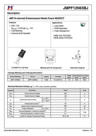
JMPF12N65BJ Description JMP N-channel Enhancement Mode Power MOSFET Features Applications 650V, 12A Load Switch RDS(ON)
jmpc12n65bj.pdf
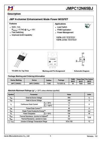
JMPC12N65BJ Description JMP N-channel Enhancement Mode Power MOSFET Features Applications 650V, 12A Load Switch RDS(ON)
lnd2n65 lnc2n65 lng2n65 lnh2n65.pdf
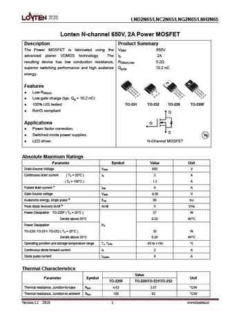
LND2N65/LNC2N65/LNG2N65/LNH2N65 Lonten N-channel 650V, 2A Power MOSFET Description Product Summary The Power MOSFET is fabricated using the VDSS 650V advanced planer VDMOS technology. The ID 2A resulting device has low conduction resistance, RDS(on),max 5.2 superior switching performance and high avalance Qg,typ 10.2 nC energy. Features Low RDS(on) Low gate charge
lnd12n65 lnc12n65 lne12n65 lnf12n65 lndn12n65.pdf
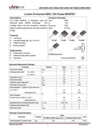
LND12N65/LNC12N65/LNE12N65/LNF12N65/LNDN12N65 Lonten N-channel 650V, 12A Power MOSFET Description Product Summary The Power MOSFET is fabricated using the V 650V DSS advanced planer VDMOS technology. The I 12A D resulting device has low conduction resistance, R 0.8 DS(on),max superior switching performance and high avalanche Q 41.9 nC g,typ energy. Features Low R DS(on)
lnd2n65 lnc2n65 lng2n65 lnh2n65 lnu2n65.pdf
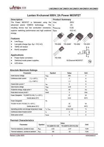
LND2N65/LNC2N65/LNG2N65/LNH2N65/LNU2N65 Lonten N-channel 650V, 2A Power MOSFET Description Product Summary The Power MOSFET is fabricated using the V 650V DSS advanced planer VDMOS technology. The I 2A D resulting device has low conduction resistance, R 5.2 DS(on),max superior switching performance and high avalance Q 10.2 nC g,typ energy. Features Low R DS(on) Low gate
lnd12n65 lnc12n65 lne12n65 lnf12n65.pdf
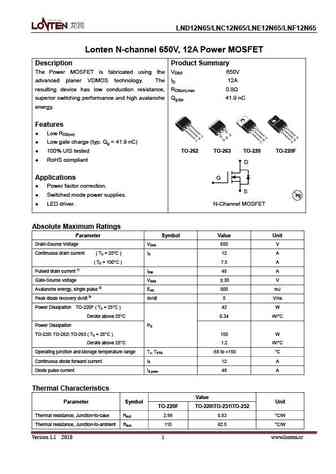
LND12N65/LNC12N65/LNE12N65/LNF12N65 Lonten N-channel 650V, 12A Power MOSFET Description Product Summary The Power MOSFET is fabricated using the VDSS 650V advanced planer VDMOS technology. The ID 12A resulting device has low conduction resistance, RDS(on),max 0.8 superior switching performance and high avalanche Qg,typ 41.9 nC energy. Features Low RDS(on) Low gate
f12n65.pdf
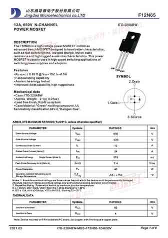
Jingdao Microelectronics co.LTD F12N65 ITO-220ABW 12A, 650V N-CHANNEL POWER MOSFET DESCRIPTION The F12N65 is a high voltage power MOSFET combines advanced trench MOSFET designed to have better characteristics, such as fast switching time, low gate charge, low on-state resistance and high rugged avalanche characteristics. This pow
d2n65.pdf
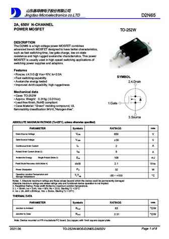
Jingdao Microelectronics co.LTD D2N65 2A, 650V N-CHANNEL POWER MOSFET TO-252W DESCRIPTION The D2N65 is a high voltage power MOSFET combines advanced trench MOSFET designed to have better characteristics, such as fast switching time, low gate charge, low on-state resistance and high rugged avalanche characteristics. This power MOSFET is usu
ptf12n65.pdf
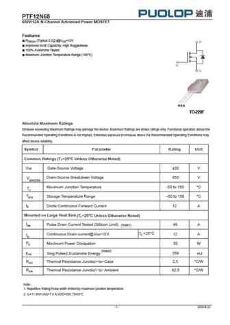
PTF1 2N65 65 0V/1 2A N-Channel A dv anced Power MOSFET Features RDS(on) (Typical 0.5 )@VGS=10V Improved dv/dt Capability, High Ruggedness 100% Avalanche Tested Maximum Junction Temperature Range (150 C) G D S TO-220F Absolute Maximum Ratings Stresses exceeding Maximum Ratings may damage the device. Maximum Ratings are stress ratings only. Functional operation above
ptf2n65.pdf
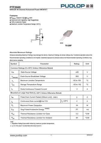
PTF2N65 65 0V/2A N-Channel A dv anced Power MOSFET Features RDS(on) (Typical 4.9 )@VGS=30V Improved dv/dt Capability, High Ruggedness 100% Avalanche Tested Maximum Junction Temperature Range (150 C) G D S TO-220F Absolute Maximum Ratings Stresses exceeding Maximum Ratings may damage the device. Maximum Ratings are stress ratings only. Functional operation above the
y2n655s.pdf
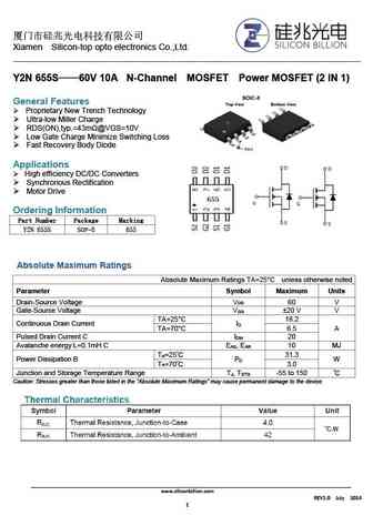
Xiamen Silicon-top opto electronics Co.,Ltd. Y2N 655S 60V 10A N-Channel MOSFET Power MOSFET (2 IN 1) General Features Proprietary New Trench Technology Ultra-low Miller Charge RDS(ON),typ.=43m @VGS=10V Low Gate Charge Minimize Switching Loss Fast Recovery Body Diode Applications High efficiency DC/DC Con
spa22n65g.pdf
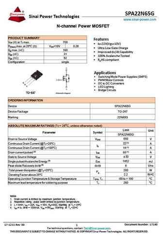
SPA22N65G Sinai Power Technologies www.sinai-power.com N-channel Power MOSFET PRODUCT SUMMARY Features V (V) at T max. 700 DS J ID=22A(Vgs=10V) R max. at 25oC ( ) V =10V 0.28 DS(on) GS Ultra Low Gate Charge Q max. (nC) 160 g Improved dv/dt Capability Q (nC) 31 gs 100% Avalanche Tested Q (nC) 52 gd ROHS compliant Configuration single
ci72n65.pdf
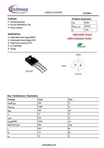
SJMOS N-MOSFET CI72N65 Features Product Summary Ultra-fast body diode VDS 650V Very low FOM RDS(on) Qg RDS(on) typ. 44m Easy to use/drive ID 72A Applications 100% DVDS Tested Switch Mode Power Supply (SMPS) 100% Avalanche Tested Uninterruptible Power Supply (UPS) Power Factor Correction (PFC) LLC Half-bridge Charger Key Performance Parame
se12n65.pdf
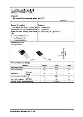
SE12N65 N-Channel Enhancement-Mode MOSFET Revision A General Description Features Thigh Density Cell Design For Ultra Low For a single MOSFET On-Resistance Fully Characterized Avalanche V =650V DS Voltage and Current Improved Shoot-Through R =630m @V =10V DS(ON) GS FOM Simple Drive Requirement Small Package Outline Surface Mount Device Pin configurations
smirf12n65.pdf
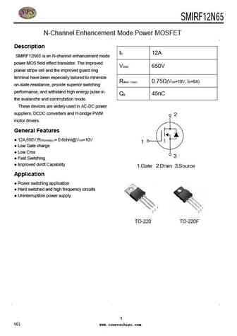
SMIRF12N65 30V /36A Single N Power MOSFET N-Channel Enhancement Mode Power MOSFET Description ID 12A SMIRF12N65 is an N-channel enhancement mode power MOS field effect transistor. The improved VDSS 650V planar stripe cell and the improved guard ring terminal have been especially tailored to minimize Rdson max 0.75 (VGS=10V, ID=6A) on-state resistance, provide superior
vbzmb12n65.pdf
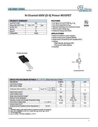
VBZMB12N65 www.VBsemi.com N-Channel 650V (D-S) Power MOSFET FEATURES PRODUCT SUMMARY VDS (V) at TJ max. 650 Low figure-of-merit (FOM) Ron x Qg Low input capacitance (Ciss) RDS(on) max. at 25 C ( ) VGS = 10 V 0.68 43 Reduced switching and conduction losses Qg max. (nC) Ultra low gate charge (Qg) 5 Qgs (nC) Avalanche energy rated (UIS) 22 Qgd (nC) Configu
vbzmb2n65.pdf
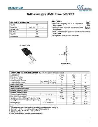
VBZMB2N65 www.VBsemi.com N-Channel (D-S) Power MOSFET 650V FEATURES PRODUCT SUMMARY Low Gate Charge Qg Results in Simple Drive VDS (V) 650 Available Requirement RDS(on) ( )VGS = 10 V 1.7 RoHS* Improved Gate, Avalanche and Dynamic dV/dt COMPLIANT Qg (Max.) (nC) 11 Ruggedness Qgs (nC) 2.3 Fully Characterized Capacitance and Avalanche Voltage and Current Qgd (nC) 5
2n65-to252.pdf
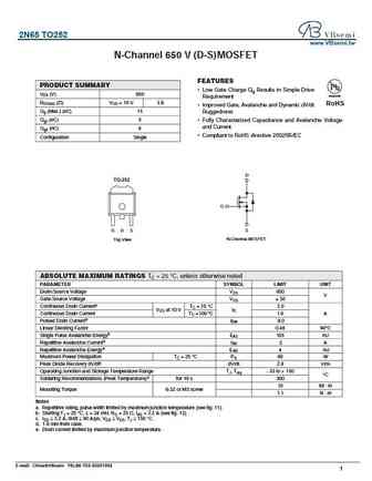
2N65 TO252 www.VBsemi.tw N-Channel 650 V (D-S) MOSFET FEATURES PRODUCT SUMMARY Low Gate Charge Qg Results in Simple Drive VDS (V) 650 Available Requirement RDS(on) ( )VGS = 10 V 3.8 RoHS Improved Gate, Avalanche and Dynamic dV/dt Qg (Max.) (nC) 15 Ruggedness Qgs (nC) 3 Fully Characterized Capacitance and Avalanche Voltage and Current Qgd (nC) 6 Compliant to Ro
tma12n65h tmp12n65h.pdf
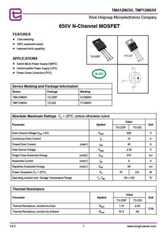
TMA12N65H, TMP12N65H Wuxi Unigroup Microelectronics Company 650V N-Channel MOSFET FEATURES Fast switching 100% avalanche tested Improved dv/dt capability APPLICATIONS Switch Mode Power Supply (SMPS) Uninterruptible Power Supply (UPS) Power Factor Correction (PFC) Device Marking and Package Information Device Package Marking TMA12N65H TO-220F A1
hm12n65 hm12n65f.pdf
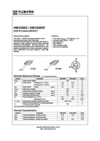
HM12N65 / HM12N65F 650V N-Channel MOSFET General Description Features This Power MOSFET is produced using SL semi s 12.0A, 650V, RDS(on) = 0.75 @VGS = 10 V advanced planar stripe DMOS technology. Low gate charge ( typical 52nC) This advanced technology has been espe cially tailored to High ruggedness minimize o n-state r esistance, pr ovide superior switching Fast w
hm2n65r.pdf
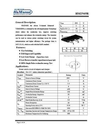
HM2N65R General Description VDSS 650 V HM2N65R the silicon N-channel Enhanced ID 2 A PD(TC=25 ) 30 W VDMOSFETs, is obtained by the self-aligned planar Technology RDS(ON)Typ 7.8 which reduce the conduction loss, improve switching performance and enhance the avalanche energy. The transistor can be used in various power switching circuit for system miniaturization and
mpf12n65.pdf
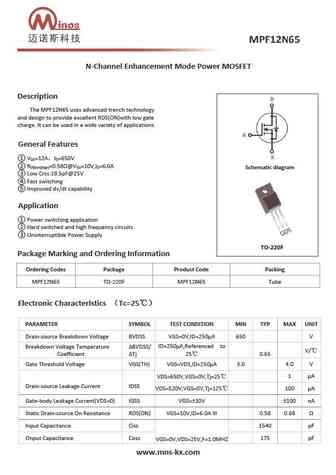
N-Channel Enhancement Mode Power MOSFET Description The MPF12N65 uses advanced trench technology and design to provide excellent RDS(ON)with low gate charge. It can be used in a wide variety of applications. General Features V =12A I =650V DS D R =0.58 @V =10V,I =6.0A DS(on)(typ) GS D Schematic diagram Low Crss 18.5pF@25V Fast switching Improved dv/dt capabil
fxn12n65f.pdf
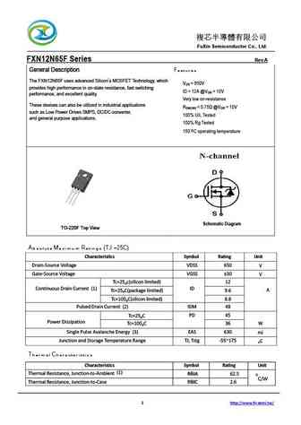
FuXin Semiconductor Co., Ltd. FXN12N65F Series Rev.A General Description Features The FXN12N65F uses advanced Silicon s MOSFET Technology, which V = 650V DS provides high performance in on-state resistance, fast switching ID = 12A @V = 10V GS performance, and excellent quality. Very low on-resistance These devices can also be utilized in ind
mpva2n65bk mpvu2n65bk mpvd2n65bk.pdf
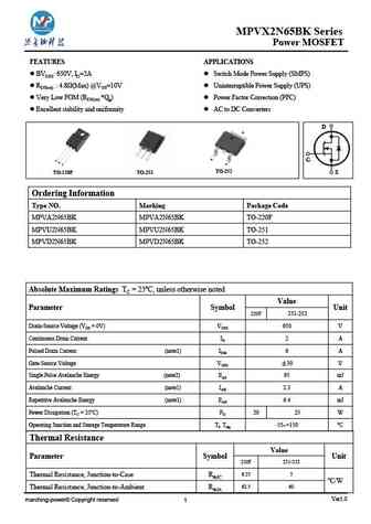
MPVX2N65BK Series Power MOSFET MPSW60M041 FEATURES APPLICATIONS BVDSS 650V, ID=2A Switch Mode Power Supply (SMPS) RDS(on) 4.8 (Max) @VGS=10V Uninterruptible Power Supply (UPS) Very Low FOM (RDS(on) *Qg) Power Factor Correction (PFC) Excellent stability and uniformity AC to DC Converters D G TO-252 TO-220F S TO-251 Ordering Information Type NO. Mark
mpva12n65f.pdf
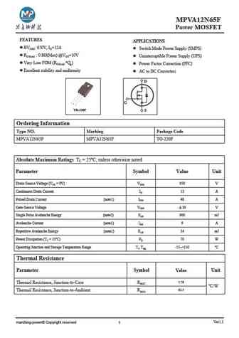
MPVA12N65F Power MOSFET MPSW60M041 FEATURES APPLICATIONS l BVDSS 650V, ID=12A l Switch Mode Power Supply (SMPS) l RDS(on) 0.8 (Max) @VGS=10V l Uninterruptible Power Supply (UPS) l Very Low FOM (RDS(on) *Qg) l Power Factor Correction (PFC) l Excellent stability and uniformity l AC to DC Converters D G TO-220F S Ordering Information Type NO. Marking Package Code MPVA12N6
h12n65p h12n65f.pdf
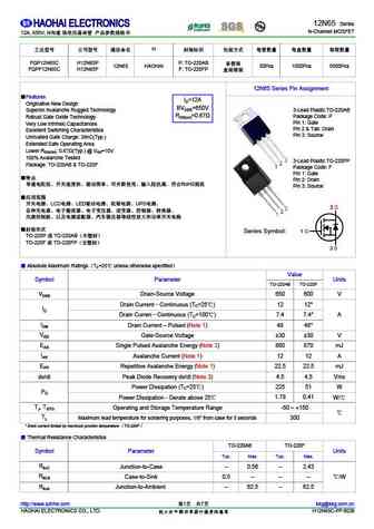
12N65 Series N-Channel MOSFET 12A, 650V, N H FQP12N65C H12N65P P TO-220AB 12N65 HAOHAI 50Pcs 1000Pcs 5000Pcs FQPF12N65C H12N65F F TO-220FP 12N65 Series Pin Assignment Features ID=12A Originative New Des
h2n65u h2n65d.pdf
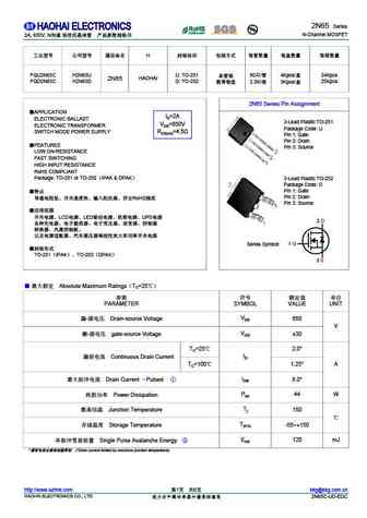
2N65 Series N-Channel MOSFET 2A, 650V, N H FQU2N65C H2N65U U TO-251 80 / 4Kpcs/ 24Kpcs HAOHAI 2N65 FQD2N65C H2N65D D TO-252 25Kpcs 2.5K/ 5Kpcs/ 2N65 Series Pin Assignment APPLICATION ID=2A
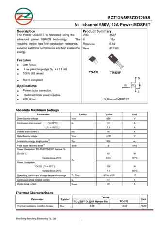
aob12n65l.pdf

isc N-Channel MOSFET Transistor AOB12N65L FEATURES Drain Current I =12A@ T =25 D C Drain Source Voltage- V =650V(Min) DSS Static Drain-Source On-Resistance R = 0.72 (Max) DS(on) 100% avalanche tested Minimum Lot-to-Lot variations for robust device performance and reliable operation DESCRIPTION Designed for use in switch mode power supplies and general purpo
aotf12n65.pdf
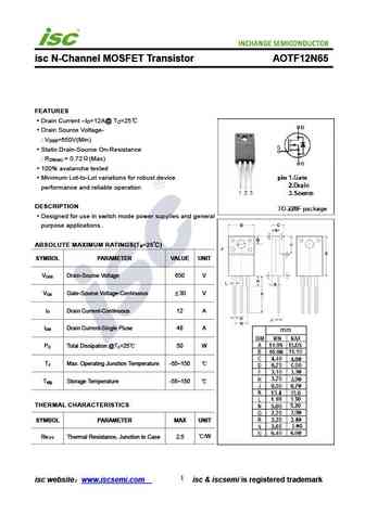
isc N-Channel MOSFET Transistor AOTF12N65 FEATURES Drain Current I =12A@ T =25 D C Drain Source Voltage- V =650V(Min) DSS Static Drain-Source On-Resistance R = 0.72 (Max) DS(on) 100% avalanche tested Minimum Lot-to-Lot variations for robust device performance and reliable operation DESCRIPTION Designed for use in switch mode power supplies and general purpo
2n6560.pdf
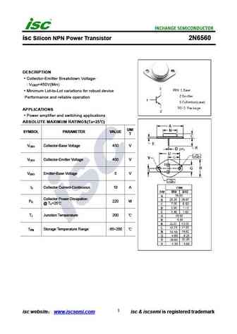
isc Silicon NPN Power Transistor 2N6560 DESCRIPTION Collector-Emitter Breakdown Voltage- V =450V(Min) CEO Minimum Lot-to-Lot variations for robust device Performance and reliable operation APPLICATIONS Power amplifier and switching applications ABSOLUTE MAXIMUM RATINGS(Ta=25 ) UNI SYMBOL PARAMETER VALUE T V Collector-Base Voltage 450 V CBO V Collector-Emitter Voltage 45
2n6583.pdf

isc Silicon NPN Power Transistor 2N6583 DESCRIPTION Excellent Safe Operating Area Collector-Emitter Sustaining Voltage- V = 400V(Min) CEO(SUS) High Current Capability Collector-Emitter Saturation Voltage- V )= 1.5 V(Max)@ I = 10A CE(sat C Minimum Lot-to-Lot variations for robust device performance and reliable operation APPLICATIONS Designed for linear amplifiers, s
2n6594.pdf
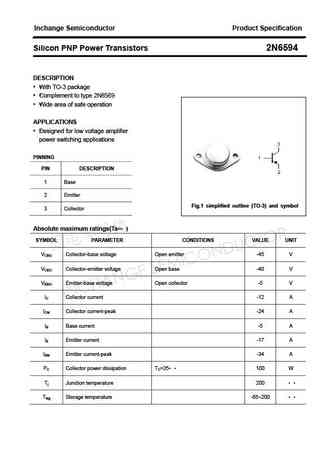
Inchange Semiconductor Product Specification Silicon PNP Power Transistors 2N6594 DESCRIPTION With TO-3 package Complement to type 2N6569 Wide area of safe operation APPLICATIONS Designed for low voltage amplifier power switching applications PINNING PIN DESCRIPTION 1 Base 2 Emitter Fig.1 simplified outline (TO-3) and symbol 3 Collector Absolute maximum ratings
ixfp22n65x2m.pdf
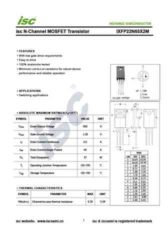
INCHANGE Semiconductor isc N-Channel MOSFET Transistor IXFP22N65X2M FEATURES With low gate drive requirements Easy to drive 100% avalanche tested Minimum Lot-to-Lot variations for robust device performance and reliable operation APPLICATIONS Switching applications ABSOLUTE MAXIMUM RATINGS(T =25 ) a SYMBOL PARAMETER VALUE UNIT V Drain-Source Voltage 650 V DSS V G
ixfp12n65x2m.pdf
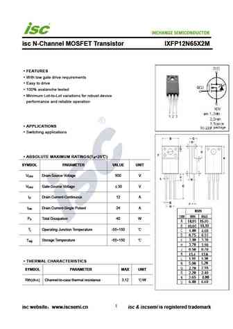
INCHANGE Semiconductor isc N-Channel MOSFET Transistor IXFP12N65X2M FEATURES With low gate drive requirements Easy to drive 100% avalanche tested Minimum Lot-to-Lot variations for robust device performance and reliable operation APPLICATIONS Switching applications ABSOLUTE MAXIMUM RATINGS(T =25 ) a SYMBOL PARAMETER VALUE UNIT V Drain-Source Voltage 650 V DSS V G
aob12n65.pdf
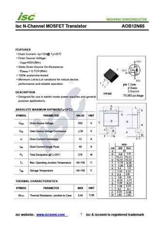
isc N-Channel MOSFET Transistor AOB12N65 FEATURES Drain Current I =12A@ T =25 D C Drain Source Voltage- V =650V(Min) DSS Static Drain-Source On-Resistance R = 0.72 (Max) DS(on) 100% avalanche tested Minimum Lot-to-Lot variations for robust device performance and reliable operation DESCRIPTION Designed for use in switch mode power supplies and general purpos
2n6561.pdf

isc Silicon NPN Power Transistor 2N6561 DESCRIPTION Collector-Emitter Breakdown Voltage- V =300V(Min) CEO Minimum Lot-to-Lot variations for robust device Performance and reliable operation APPLICATIONS Power amplifier and switching applications ABSOLUTE MAXIMUM RATINGS(Ta=25 ) UNI SYMBOL PARAMETER VALUE T V Collector-Base Voltage 300 V CBO V Collector-Emitter Voltage 30
2n6576 2n6577 2n6578.pdf
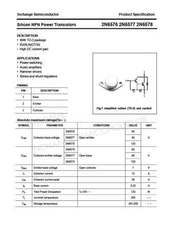
Inchange Semiconductor Product Specification Silicon NPN Power Transistors 2N6576 2N6577 2N6578 DESCRIPTION With TO-3 package DARLINGTON High DC current gain APPLICATIONS Power switching Audio amplifiers Hammer drivers Series and shunt regulators PINNING PIN DESCRIPTION 1 Base 2 Emitter Fig.1 simplified outline (TO-3) and symbol 3 Collector Absolute
2n6500.pdf
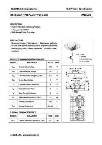
INCHANGE Semiconductor isc Product Specification isc Silicon NPN Power Transistor 2N6500 DESCRIPTION Collector-Emitter Sustaining Voltage- VCEO(SUS)= 90V(Min) Wide Area of Safe Operation APPLICATIONS Designed for use in high-current, high-speed switching circuits such as low-distortion power amplifiers,oscillators, switching regulators, series regulators, converters
ntp082n65s3f.pdf
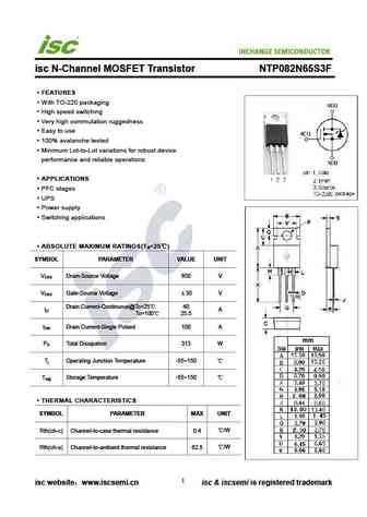
INCHANGE Semiconductor isc N-Channel MOSFET Transistor NTP082N65S3F FEATURES With TO-220 packaging High speed switching Very high commutation ruggedness Easy to use 100% avalanche tested Minimum Lot-to-Lot variations for robust device performance and reliable operationz APPLICATIONS PFC stages UPS Power supply Switching applications ABSOLUTE MAXIMUM RATI
ixfp12n65x2.pdf
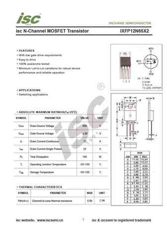
isc N-Channel MOSFET Transistor IXFP12N65X2 FEATURES With low gate drive requirements Easy to drive 100% avalanche tested Minimum Lot-to-Lot variations for robust device performance and reliable operation APPLICATIONS Switching applications ABSOLUTE MAXIMUM RATINGS(T =25 ) a SYMBOL PARAMETER VALUE UNIT V Drain-Source Voltage 650 V DSS V Gate-Source Voltage 30 V
2n6584.pdf

isc Silicon NPN Power Transistor 2N6584 DESCRIPTION Excellent Safe Operating Area Collector-Emitter Sustaining Voltage- V = 450V(Min) CEO(SUS) High Current Capability Collector-Emitter Saturation Voltage- V )= 1.5 V(Max)@ I = 10A CE(sat C Minimum Lot-to-Lot variations for robust device performance and reliable operation APPLICATIONS Designed for linear amplifiers, s
2n6536.pdf
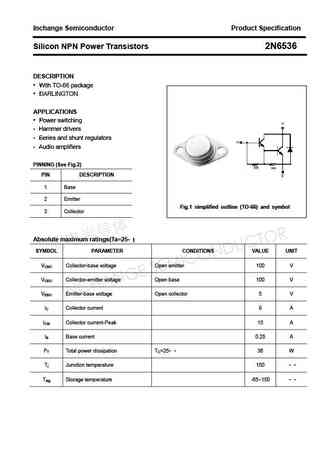
Inchange Semiconductor Product Specification Silicon NPN Power Transistors 2N6536 DESCRIPTION With TO-66 package DARLINGTON APPLICATIONS Power switching Hammer drivers Series and shunt regulators Audio amplifiers PINNING (See Fig.2) PIN DESCRIPTION 1 Base 2 Emitter Fig.1 simplified outline (TO-66) and symbol 3 Collector Absolute maximum ratings(Ta=25 )
2n6582.pdf
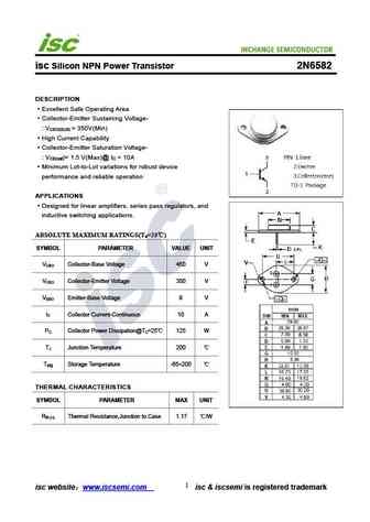
isc Silicon NPN Power Transistor 2N6582 DESCRIPTION Excellent Safe Operating Area Collector-Emitter Sustaining Voltage- V = 350V(Min) CEO(SUS) High Current Capability Collector-Emitter Saturation Voltage- V )= 1.5 V(Max)@ I = 10A CE(sat C Minimum Lot-to-Lot variations for robust device performance and reliable operation APPLICATIONS Designed for linear amplifiers, s
2n6575.pdf
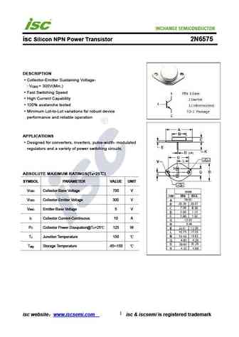
isc Silicon NPN Power Transistor 2N6575 DESCRIPTION Collector-Emitter Sustaining Voltage- V = 300V(Min.) CEO Fast Switching Speed High Current Capability 100% avalanche tested Minimum Lot-to-Lot variations for robust device performance and reliable operation APPLICATIONS Designed for converters, inverters, pulse-width- modulated regulators and a variety of power switch
2n6542 2n6543.pdf
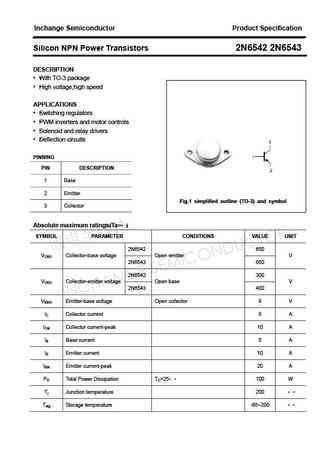
Inchange Semiconductor Product Specification Silicon NPN Power Transistors 2N6542 2N6543 DESCRIPTION With TO-3 package High voltage,high speed APPLICATIONS Switching regulators PWM inverters and motor controls Solenoid and relay drivers Deflection circuits PINNING PIN DESCRIPTION 1 Base 2 Emitter Fig.1 simplified outline (TO-3) and symbol 3 Collector Abs
12n65kl-tf1-t.pdf
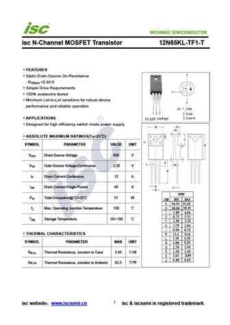
isc N-Channel MOSFET Transistor 12N65KL-TF1-T FEATURES Static Drain-Source On-Resistance R
2n6546 2n6547.pdf
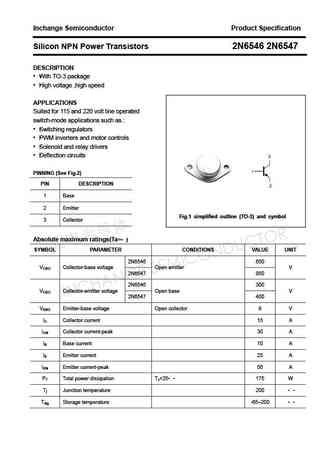
Inchange Semiconductor Product Specification Silicon NPN Power Transistors 2N6546 2N6547 DESCRIPTION With TO-3 package High voltage ,high speed APPLICATIONS Suited for 115 and 220 volt line operated switch-mode applications such as Switching regulators PWM inverters and motor controls Solenoid and relay drivers Deflection circuits PINNING (See Fig.2) PIN
2n6574.pdf
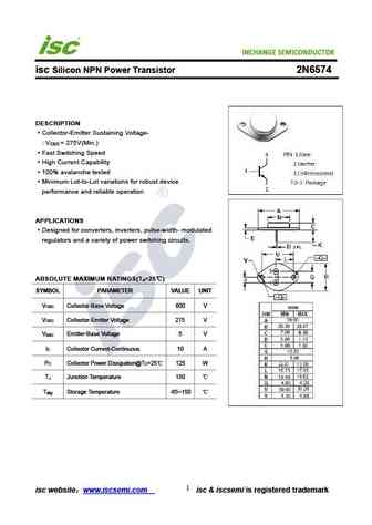
isc Silicon NPN Power Transistor 2N6574 DESCRIPTION Collector-Emitter Sustaining Voltage- V = 275V(Min.) CEO Fast Switching Speed High Current Capability 100% avalanche tested Minimum Lot-to-Lot variations for robust device performance and reliable operation APPLICATIONS Designed for converters, inverters, pulse-width- modulated regulators and a variety of power switch
ixfa22n65x2.pdf
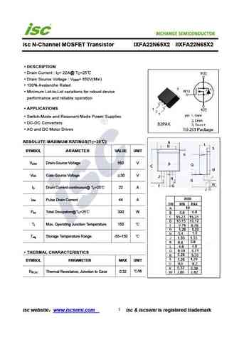
INCHANGE Semiconductor isc N-Channel MOSFET Transistor IXFA22N65X2 IIXFA22N65X2 DESCRIPTION Drain Current I = 22A@ T =25 D C Drain Source Voltage V = 650V(Min) DSS 100% Avalanche Rated Minimum Lot-to-Lot variations for robust device performance and reliable operation APPLICATIONS . Switch-Mode and Resonant-Mode Power Supplies DC-DC Converters AC and DC Moto
2n6544.pdf

isc Silicon NPN Power Transistor 2N6544 DESCRIPTION Excellent Safe Operating Area High Voltage,High Speed Low Saturation Voltage Minimum Lot-to-Lot variations for robust device performance and reliable operation APPLICATIONS Switching regulators PWM inverters and motor controls Solenoid and relay drivers Deflection circuits ABSOLUTE MAXIMUM RATINGS(T =25 ) a SYMB
ixfp22n65x2.pdf
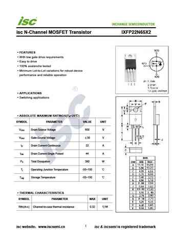
INCHANGE Semiconductor isc N-Channel MOSFET Transistor IXFP22N65X2 FEATURES With low gate drive requirements Easy to drive 100% avalanche tested Minimum Lot-to-Lot variations for robust device performance and reliable operation APPLICATIONS Switching applications ABSOLUTE MAXIMUM RATINGS(T =25 ) a SYMBOL PARAMETER VALUE UNIT V Drain-Source Voltage 650 V DSS V Ga
aow12n65.pdf
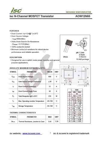
isc N-Channel MOSFET Transistor AOW12N65 FEATURES Drain Current I =12A@ T =25 D C Drain Source Voltage- V =650V(Min) DSS Static Drain-Source On-Resistance R = 0.72 (Max) DS(on) 100% avalanche tested Minimum Lot-to-Lot variations for robust device performance and reliable operation DESCRIPTION Designed for use in switch mode power supplies and general purpos
2n6573.pdf

isc Silicon NPN Power Transistor 2N6573 DESCRIPTION Collector-Emitter Sustaining Voltage- V = 250V(Min.) CEO Fast Switching Speed High Current Capability 100% avalanche tested Minimum Lot-to-Lot variations for robust device performance and reliable operation APPLICATIONS Designed for converters, inverters, pulse-width- modulated regulators and a variety of power switch
aot12n65.pdf
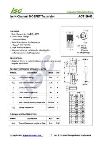
isc N-Channel MOSFET Transistor AOT12N65 FEATURES Drain Current I =12A@ T =25 D C Drain Source Voltage- V =650V(Min) DSS Static Drain-Source On-Resistance R = 0.72 (Max) DS(on) 100% avalanche tested Minimum Lot-to-Lot variations for robust device performance and reliable operation DESCRIPTION Designed for use in switch mode power supplies and general purpos
2n6537.pdf
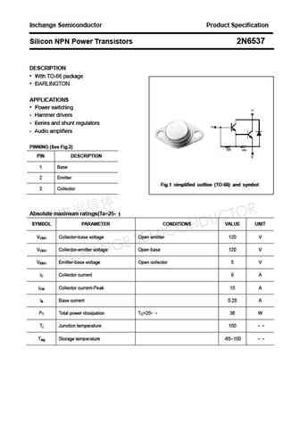
Inchange Semiconductor Product Specification Silicon NPN Power Transistors 2N6537 DESCRIPTION With TO-66 package DARLINGTON APPLICATIONS Power switching Hammer drivers Series and shunt regulators Audio amplifiers PINNING (See Fig.2) PIN DESCRIPTION 1 Base 2 Emitter Fig.1 simplified outline (TO-66) and symbol 3 Collector Absolute maximum ratings(Ta=25 )
ntb082n65s3f.pdf
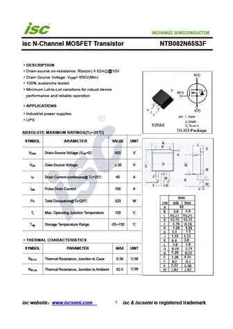
INCHANGE Semiconductor isc N-Channel MOSFET Transistor NTB082N65S3F DESCRIPTION Drain-source on-resistance RDS(on) 82m @10V Drain Source Voltage V = 650V(Min) DSS 100% avalanche tested Minimum Lot-to-Lot variations for robust device performance and reliable operation APPLICATIONS . Industrial power supplies UPS ABSOLUTE MAXIMUM RATINGS(T =25 ) C SYMBOL AR
2n6569.pdf
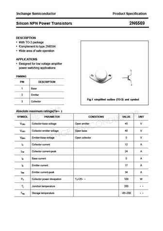
Inchange Semiconductor Product Specification Silicon NPN Power Transistors 2N6569 DESCRIPTION With TO-3 package Complement to type 2N6594 Wide area of safe operation APPLICATIONS Designed for low voltage amplifier power switching applications PINNING PIN DESCRIPTION 1 Base 2 Emitter Fig.1 simplified outline (TO-3) and symbol 3 Collector Absolute maximum rating
2n6545.pdf
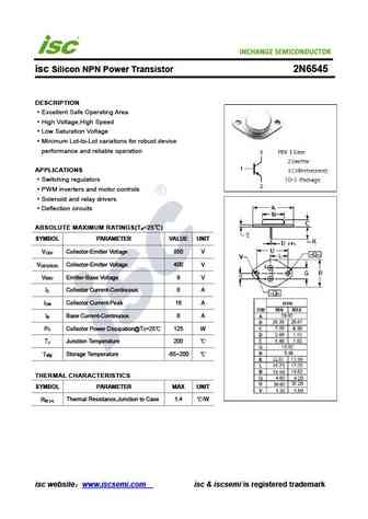
isc Silicon NPN Power Transistor 2N6545 DESCRIPTION Excellent Safe Operating Area High Voltage,High Speed Low Saturation Voltage Minimum Lot-to-Lot variations for robust device performance and reliable operation APPLICATIONS Switching regulators PWM inverters and motor controls Solenoid and relay drivers Deflection circuits ABSOLUTE MAXIMUM RATINGS(T =25 ) a SYMB
2n6579.pdf
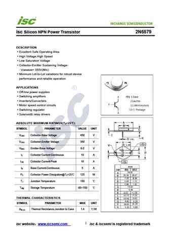
INCHANGE Semiconductor isc Silicon NPN Power Transistor 2N6579 DESCRIPTION Excellent Safe Operating Area High Voltage,High Speed Low Saturation Voltage Collector-Emitter Sustaining Voltage- V = 350V(Min) CEO(SUS) Minimum Lot-to-Lot variations for robust device performance and reliable operation APPLICATIONS Off-line power supplies Switching amplifiers Inverters/C
aotf12n65l.pdf
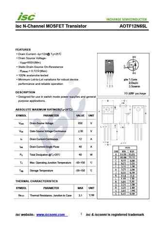
isc N-Channel MOSFET Transistor AOTF12N65L FEATURES Drain Current I =12A@ T =25 D C Drain Source Voltage- V =650V(Min) DSS Static Drain-Source On-Resistance R = 0.72 (Max) DS(on) 100% avalanche tested Minimum Lot-to-Lot variations for robust device performance and reliable operation DESCRIPTION Designed for use in switch mode power supplies and general purp
ntpf082n65s3f.pdf
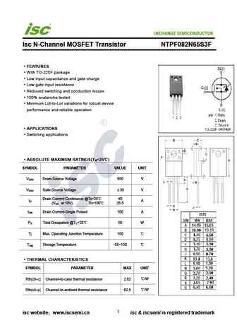
INCHANGE Semiconductor Isc N-Channel MOSFET Transistor NTPF082N65S3F FEATURES With TO-220F package Low input capacitance and gate charge Low gate input resistance Reduced switching and conduction losses 100% avalanche tested Minimum Lot-to-Lot variations for robust device performance and reliable operation APPLICATIONS Switching applications ABSOLUTE MAXIMUM RATI
12n65tf.pdf
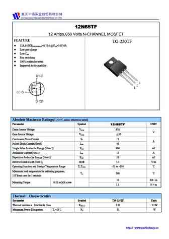
12N65TF 12 Amps,650 Volts N-CHANNEL MOSFET FEATURE TO-220TF 12A,650V,R =0.75 @V =10V/6A DS(ON)MAX GS Low gate charge Low C iss Fast switching 100% avalanche tested Improved dv/dt capability Absolute Maximum Ratings(T =25 ,unless otherwise noted) C Parameter Symbol UNIT 12N65TF Drain-Source Voltage V 650 DSS V Gate-Source Voltage V 30 GSS Continu
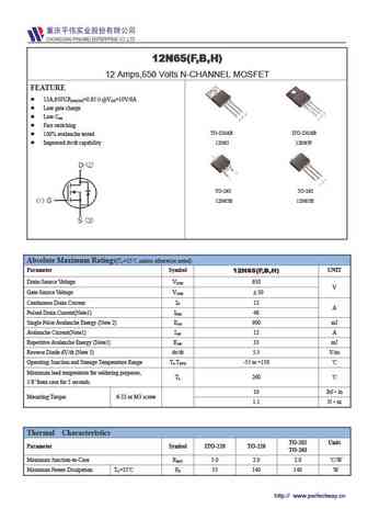
ap12n65f ap12n65p.pdf
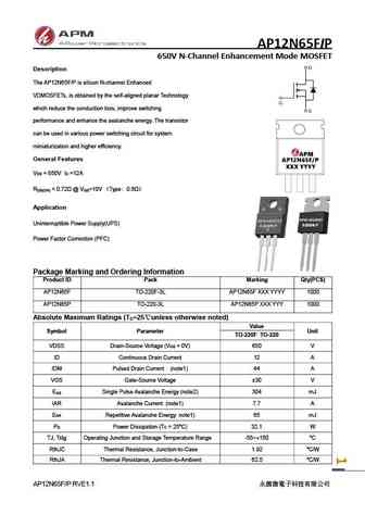
AP12N65FIP 650V N-Channel Enhancement Mode MOSFET Description The AP12N65F/P is silicon N-channel Enhanced VDMOSFETs, is obtained by the self-aligned planar Technology which reduce the conduction loss, improve switching performance and enhance the avalanche energy. The transistor can be used in various power switching circuit for system miniaturization and higher efficiency.
Другие IGBT... 10N65Z, 10N65K, 15N65, 18N65, 20N65, 22N65, 1N65A, 1N65, IRF520, 2N65L, 2N65Z, 2N65K, 3N65A, 3N65, 3N65Z, 3N65K, 4N65
Параметры MOSFET. Взаимосвязь и компромиссы
🌐 : EN ES РУ

Список транзисторов
Обновления
MOSFET: BLM3404 | BL4N90 | SI2309S | SI2301F | BMSN3139 | BMS2302 | BMS2301 | BMDFN2302 | BMDFN2301 | BM8205 | BM3139KT | BM3134KE | BM3134E | AO3415E | AO3401F | CS65N25AKR
Popular searches
2sa992 | 2sa970 | a970 | d2390 transistor | 2n5087 equivalent | tip147 datasheet | 2n4124 | mj15022