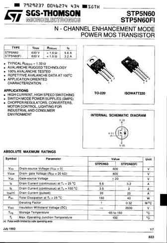
5N60 datasheet, аналоги, основные параметры
Наименование производителя: 5N60 📄📄
Тип транзистора: MOSFET
Полярность: N
Предельные значения
Pd ⓘ - Максимальная рассеиваемая мощность: 100 W
|Vds|ⓘ - Максимально допустимое напряжение сток-исток: 600 V
|Vgs|ⓘ - Максимально допустимое напряжение затвор-исток: 30 V
|Id| ⓘ - Максимально допустимый постоянный ток стока: 5 A
Tj ⓘ - Максимальная температура канала: 150 °C
Электрические характеристики
tr ⓘ - Время нарастания: 42 ns
Cossⓘ - Выходная емкость: 55 pf
RDSonⓘ - Сопротивление сток-исток открытого транзистора: 1.8 Ohm
📄📄 Копировать
Аналог (замена) для 5N60
- подборⓘ MOSFET транзистора по параметрам
5N60 даташит
5n60.pdf
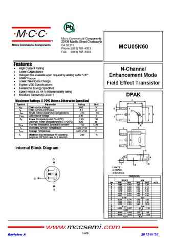
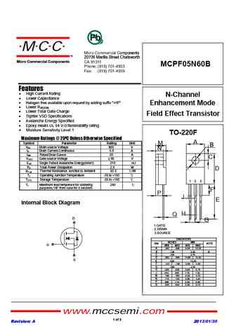
UNISONIC TECHNOLOGIES CO., LTD 5N60 Power MOSFET 5A, 600V N-CHANNEL POWER MOSFET DESCRIPTION The UTC 5N60 is a high voltage power MOSFET and is designed to have better characteristics, such as fast switching time, low gate charge, low on-state resistance and have a high rugged avalanche characteristics. This power MOSFET is usually used at high speed switching applications
5n60 5n60f.pdf
GOFORD 5N60/5N60F 600V N-Channel MOSFET GENERAL DESCRIPTION VDSS RDS(ON) ID This Power MOSFET is produced using advanced planar stripe, DMOS 600V 2.5 4.5A technology.This latest technology has been especially designed to minimize on-state resistance, have a high rugged avalanche characteristics, such as fast switching time,low on resistance.low gate charge and especially excellen
5n60.pdf
INCHANGE Semiconductor isc N-Channel MOSFET Transistor 5N60 DESCRIPTION Drain Current I = 5.6A@ T =25 D C Drain Source Voltage V = 600V(Min) DSS Fast Switching Speed Minimum Lot-to-Lot variations for robust device performance and reliable operation APPLICATIONS AC Adapter, Battery Charge and SMPS ABSOLUTE MAXIMUM RATINGS(T =25 ) C SYMBOL ARAMETER VALUE UNIT
fgy75n60smd.pdf
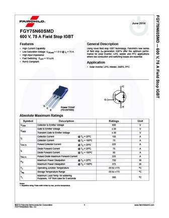
June 2014 FGY75N60SMD 600 V, 75 A Field Stop IGBT Features General Description High Current Capability Using novel field stop IGBT technology, Fairchild s new series of field stop 2nd generation IGBTs offer the optimum perfor- Low Saturation Voltage VCE(sat) = 1.9 V @ IC = 75 A mance for solar inverter, UPS, welder and PFC applications High Input Impedance where low co
nvhl055n60s5f.pdf
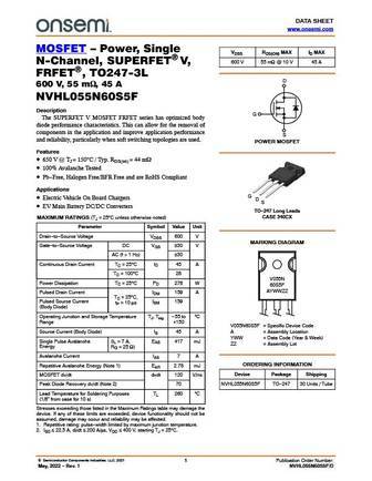
DATA SHEET www.onsemi.com MOSFET Power, Single VDSS RDS(ON) MAX ID MAX 600 V 55 mW @ 10 V 45 A N-Channel, SUPERFET) V, FRFET), TO247-3L D 600 V, 55 mW, 45 A NVHL055N60S5F Description G The SUPERFET V MOSFET FRFET series has optimized body diode performance characteristics. This can allow for the removal of components in the application and improve application performance S a
ssg55n60.pdf
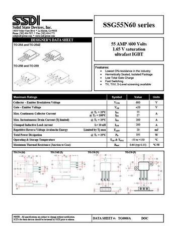
SSG55N60 series Solid State Devices, Inc. 14830 Valley View Blvd * La Mirada, Ca 90638 Phone (562) 404-7855 * Fax (562) 404-1773 ssdi@ssdi-power.com * www.ssdi-power.com DESIGNER S DATA SHEET 55 AMP /600 Volts TO-254 and TO-254Z 1.65 V saturation ultrafast IGBT TO-258 and TO-259 Features Lowest ON-resistance in the industry Hermetically Sealed, Isolated Pa
tsp5n60m tsf5n60m.pdf
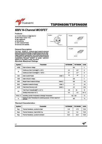
TSP5N60M/TSF5N60M 600V N-Channel MOSFET Features 4.5A,600v,RDS(on)=2.2 @VGS=10V Gate charge (Typical 17nC) High ruggedness Fast switching 100% AvalancheTested Improved dv/dt capability General Description This Power MOSFET is produced using Truesemi s advanced planar stripe, DMOS technology.This latest technology has been especially designed t
fcp165n60e.pdf

December 2015 FCP165N60E N-Channel SuperFET II Easy-Drive MOSFET 600 V, 23 A, 165 m Features Description 650 V @TJ = 150 C SuperFET II MOSFET is Fairchild Semiconductor s brand-new high voltage super-junction (SJ) MOSFET family that is utilizing Typ. RDS(on) = 132 m charge balance technology for outstanding low on-resistance Ultra Low Gate Charge (Typ. Qg = 5
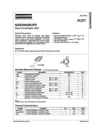
sgs5n60ruf.pdf
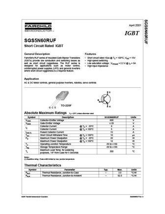
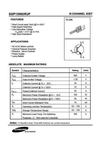
April 2001 IGBT SGS5N60RUF Short Circuit Rated IGBT General Description Features Fairchild's RUF series of Insulated Gate Bipolar Transistors Short circuit rated 10us @ TC = 100 C, VGE = 15V (IGBTs) provide low conduction and switching losses as High speed switching well as short circuit ruggedness. The RUF series is Low saturation voltage VCE(sat) = 2.2 V @ IC = 5A des
sgr5n60ruf.pdf
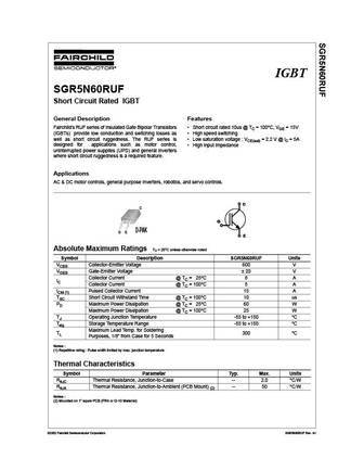
IGBT SGR5N60RUF Short Circuit Rated IGBT General Description Features Fairchild's RUF series of Insulated Gate Bipolar Transistors Short circuit rated 10us @ TC = 100 C, VGE = 15V (IGBTs) provide low conduction and switching losses as High speed switching well as short circuit ruggedness. The RUF series is Low saturation voltage VCE(sat) = 2.2 V @ IC = 5A designed for ap
xnf15n60t.pdf
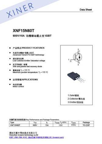
Data Sheet XNF15N60T 600V/15A IGBT /PRODUCT FEATURES 2 + Advanced Trench+FS IGBT technology 1 Low Collector-Emitter Saturation voltage 3 With anti-parallel fast recovery diode TJ = 175 C Maximum junction temperature TJ
fcp125n60e.pdf
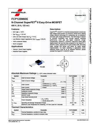
November 2015 FCP125N60E N-Channel SuperFET II Easy-Drive MOSFET 600 V, 29 A, 125 m Features Description 650 V @TJ = 150 C SuperFET II MOSFET is Fairchild Semiconductor s brand-new high voltage super-junction (SJ) MOSFET family that is utilizing Typ. RDS(on) = 102 m charge balance technology for outstanding low on-resistance Ultra Low Gate Charge (Typ. Qg = 7
svf5n60t svf5n60f svf5n60d svf5n60mj.pdf
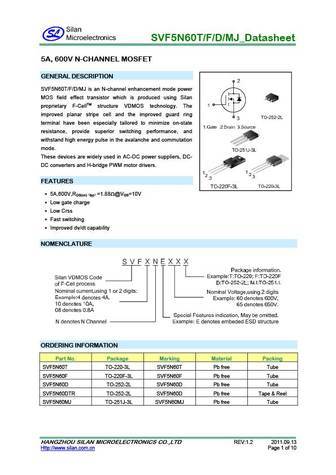
SVF5N60T/F/D/MJ_Datasheet 5A, 600V N-CHANNEL MOSFET GENERAL DESCRIPTION SVF5N60T/F/D/MJ is an N-channel enhancement mode power MOS field effect transistor which is produced using Silan proprietary F-CellTM structure VDMOS technology. The improved planar stripe cell and the improved guard ring terminal have been especially tailored to minimize on-state resistance, provide superior
mgs05n60drev0.pdf
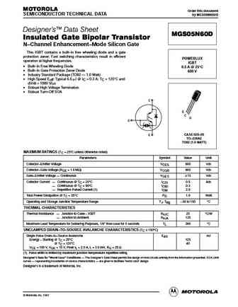
MOTOROLA Order this document SEMICONDUCTOR TECHNICAL DATA by MGS05N60D/D Designer's Data Sheet MGS05N60D Insulated Gate Bipolar Transistor N Channel Enhancement Mode Silicon Gate This IGBT contains a built in free wheeling diode and a gate protection zener. Fast switching characteristics result in efficient POWERLUX operation at higher frequencies. IGBT Built In Free
mgp5n60e.pdf
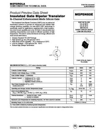
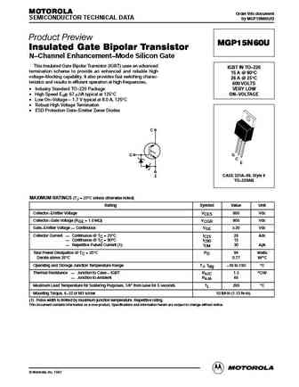
MOTOROLA Order this document SEMICONDUCTOR TECHNICAL DATA by MGP5N60E/D Product Preview Data Sheet MGP5N60E Insulated Gate Bipolar Transistor N Channel Enhancement Mode Silicon Gate IGBT IN TO 220 This Insulated Gate Bipolar Transistor (IGBT) uses an advanced 5 A @ 90 C termination scheme to provide an enhanced and reliable high 6 A @ 25 C voltage blocking capability. Its new
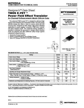
mty25n60e.pdf

MOTOROLA Order this document SEMICONDUCTOR TECHNICAL DATA by MTY25N60E/D Designer's Data Sheet MTY25N60E TMOS E-FET. Motorola Preferred Device Power Field Effect Transistor N Channel Enhancement Mode Silicon Gate TMOS POWER FET This advanced TMOS power FET is designed to withstand high 25 AMPERES energy in the avalanche and commutation modes. This new energy 600 VOLTS e
mgp15n60u.pdf
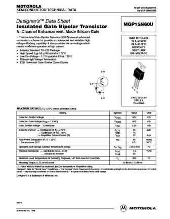
MOTOROLA Order this document SEMICONDUCTOR TECHNICAL DATA by MGP15N60U/D Designer's Data Sheet MGP15N60U Insulated Gate Bipolar Transistor N Channel Enhancement Mode Silicon Gate This Insulated Gate Bipolar Transistor (IGBT) uses an advanced IGBT IN TO 220 termination scheme to provide an enhanced and reliable high 15 A @ 90 C voltage blocking capability. It also provide
mty25n60erev2x.pdf
MOTOROLA Order this document SEMICONDUCTOR TECHNICAL DATA by MTY25N60E/D Designer's Data Sheet MTY25N60E TMOS E-FET. Motorola Preferred Device Power Field Effect Transistor N Channel Enhancement Mode Silicon Gate TMOS POWER FET This advanced TMOS power FET is designed to withstand high 25 AMPERES energy in the avalanche and commutation modes. This new energy 600 VOLTS e
mgp15n60urev0.pdf
MOTOROLA Order this document SEMICONDUCTOR TECHNICAL DATA by MGP15N60U/D Product Preview MGP15N60U Insulated Gate Bipolar Transistor N Channel Enhancement Mode Silicon Gate This Insulated Gate Bipolar Transistor (IGBT) uses an advanced IGBT IN TO 220 termination scheme to provide an enhanced and reliable high 15 A @ 90 C voltage blocking capability. It also provides fast sw
mmg05n60drev0.pdf
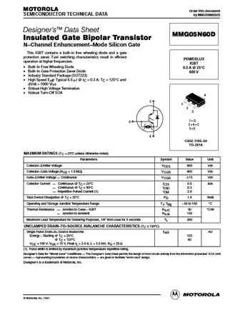
MOTOROLA Order this document SEMICONDUCTOR TECHNICAL DATA by MMG05N60D/D Designer's Data Sheet MMG05N60D Insulated Gate Bipolar Transistor N Channel Enhancement Mode Silicon Gate This IGBT contains a built in free wheeling diode and a gate protection zener. Fast switching characteristics result in efficient POWERLUX operation at higher frequencies. IGBT Built In Free
irfp15n60lpbf.pdf
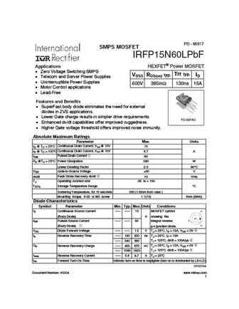
PD - 95517 SMPS MOSFET IRFP15N60LPbF Applications HEXFET Power MOSFET Zero Voltage Switching SMPS Trr typ. VDSS RDS(on) typ. ID Telecom and Server Power Supplies Uninterruptible Power Supplies 600V 385m 130ns 15A Motor Control applications Lead-Free Features and Benefits SuperFast body diode eliminates the need for external diodes in ZVS applications.
irfba35n60c.pdf
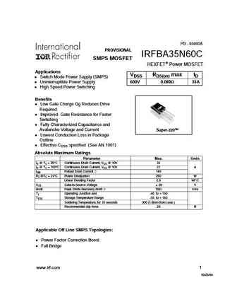
PD - 93800A PROVISIONAL IRFBA35N60C SMPS MOSFET HEXFET Power MOSFET Applications VDSS RDS(on) max ID Switch Mode Power Supply (SMPS) Uninterruptible Power Supply 600V 0.080 35A High Speed Power Switching Benefits Low Gate Charge Qg Reduces Drive Required Improved Gate Resistance for Faster Switching Fully Characterized Capacitance and Avalanche Voltage and Current Sup
irfp15n60l.pdf
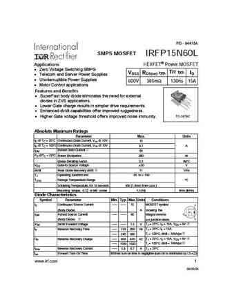
PD - 94415A SMPS MOSFET IRFP15N60L Applications HEXFET Power MOSFET Zero Voltage Switching SMPS Trr typ. VDSS RDS(on) typ. ID Telecom and Server Power Supplies Uninterruptible Power Supplies 600V 385m 130ns 15A Motor Control applications Features and Benefits SuperFast body diode eliminates the need for external diodes in ZVS applications. Lower Gate c
stw25n60m2-ep.pdf
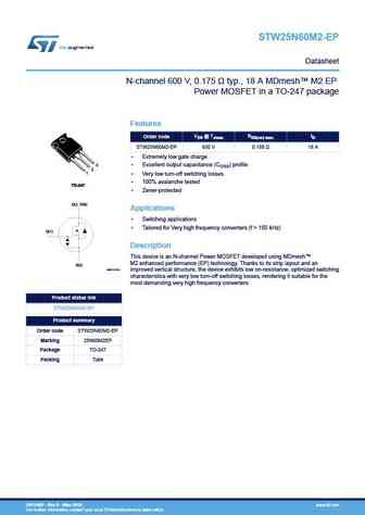
STW25N60M2-EP Datasheet N-channel 600 V, 0.175 typ., 18 A MDmesh M2 EP Power MOSFET in a TO-247 package Features VDS @ TJmax RDS(on) max. ID Order code STW25N60M2-EP 650 V 0.188 18 A Extremely low gate charge 3 Excellent output capacitance (COSS) profile 2 1 Very low turn-off switching losses 100% avalanche tested TO-247 Zener-protected D(2, TAB)
stb5n60b.pdf
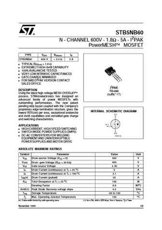
STB5NB60 N - CHANNEL 600V - 1.8 - 5A- I2PAK PowerMESH MOSFET TYPE VDSS RDS(on) ID STB5NB60 600 V
stw35n60dm2.pdf
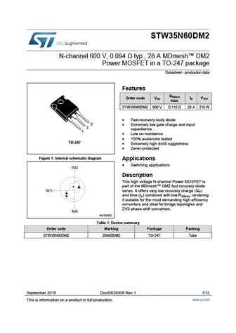
STW35N60DM2 N-channel 600 V, 0.094 typ., 28 A MDmesh DM2 Power MOSFET in a TO-247 package Datasheet - production data Features R DS(on) Order code VDS ID PTOT max. STW35N60DM2 600 V 0.110 28 A 210 W Fast-recovery body diode 3 Extremely low gate charge and input 2 capacitance 1 Low on-resistance 100% avalanche tested TO-247 Extremely
stw45n60dm2ag.pdf
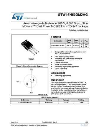
STW45N60DM2AG Automotive-grade N-channel 600 V, 0.085 typ., 34 A MDmesh DM2 Power MOSFET in a TO-247 package Datasheet - production data Features V @ R DS DS(on) Order code I P D TOT TJmax. max. 34 250 STW45N60DM2AG 650 V 0.093 A W 3 Designed for automotive applications and 2 AEC-Q101 qualified 1 Fast-recovery body diode Extremely low gate c
std5n60m2 stp5n60m2 stu5n60m2.pdf
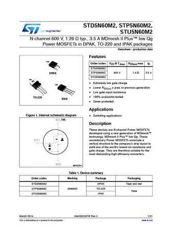
STD5N60M2, STP5N60M2, STU5N60M2 N-channel 600 V, 1.26 typ., 3.5 A MDmesh II Plus low Qg Power MOSFETs in DPAK, TO-220 and IPAK packages Datasheet - production data Features TAB Order codes VDS @ TJmax RDS(on) max ID 3 STD5N60M2 1 STP5N60M2 650 V 1.4 3.5 A DPAK STU5N60M2 TAB Extremely low gate charge TAB Lower RDS(on) x area vs previous generation 3 3 Lo
stf15n60m2-ep stfi15n60m2-ep.pdf
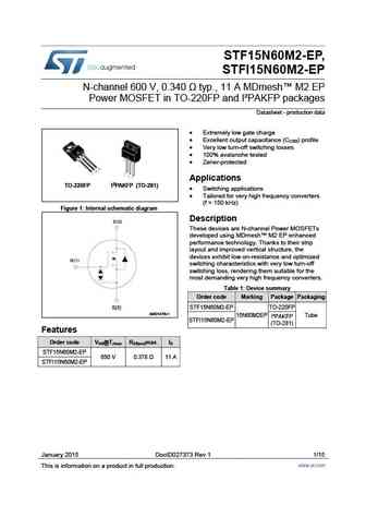
STF15N60M2-EP, STFI15N60M2-EP N-channel 600 V, 0.340 typ., 11 A MDmesh M2 EP Power MOSFET in TO-220FP and I PAKFP packages Datasheet - production data Extremely low gate charge Excellent output capacitance (COSS) profile Very low turn-off switching losses 100% avalanche tested Zener-protected Applications TO-220FP I2PAKFP (TO-281) Switching
stf5n60m2.pdf
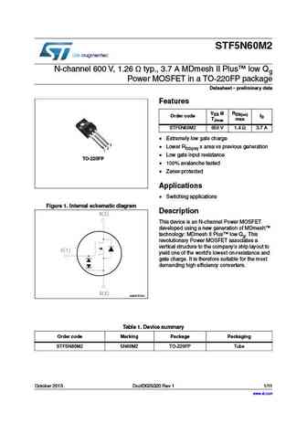
STF5N60M2 N-channel 600 V, 1.26 typ., 3.7 A MDmesh II Plus low Qg Power MOSFET in a TO-220FP package Datasheet - preliminary data Features VDS @ RDS(on) Order code ID TJmax max STF5N60M2 650 V 1.4 3.7 A Extremely low gate charge 3 Lower RDS(on) x area vs previous generation 2 1 Low gate input resistance TO-220FP 100% avalanche tested Zener-protec
stw75n60m6.pdf
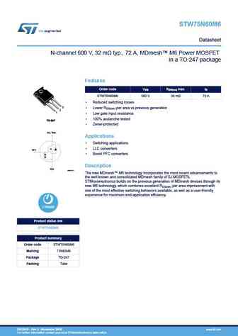
STW75N60M6 Datasheet N-channel 600 V, 32 m typ., 72 A, MDmesh M6 Power MOSFET in a TO 247 package Features VDS RDS(on) max. ID Order code STW75N60M6 600 V 36 m 72 A Reduced switching losses 3 Lower RDS(on) per area vs previous generation 2 1 Low gate input resistance 100% avalanche tested TO-247 Zener-protected D(2, TAB) Applications Switchin
stp45n60dm6 stw45n60dm6.pdf
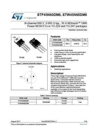
STP45N60DM6, STW45N60DM6 N-channel 600 V, 0.085 typ., 30 A MDmesh DM6 Power MOSFETs in TO-220 and TO-247 packages Datasheet - production data Features TAB Order code V R max. I DS DS(on) D STP45N60DM6 600 V 0.099 30 A STW45N60DM6 3 3 Fast-recovery body diode 2 2 1 Lower R x area vs previous generation DS(on) 1 Low gate charge, input capacitan
std5n60dm2.pdf
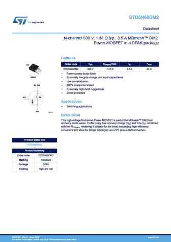
STD5N60DM2 Datasheet N-channel 600 V, 1.38 typ., 3.5 A MDmesh DM2 Power MOSFET in a DPAK package Features VDS RDS(on) max. ID PTOT Order code TAB STD5N60DM2 600 V 1.55 3.5 A 45 W 3 2 1 Fast-recovery body diode DPAK Extremely low gate charge and input capacitance Low on-resistance D(2, TAB) 100% avalanche tested Extremely high dv/dt ruggedness
stb35n60dm2.pdf
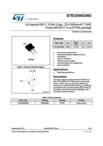
STB35N60DM2 N-channel 600 V, 0.094 typ., 28 A MDmesh DM2 Power MOSFET in a D PAK package Datasheet - production data Features R DS(on) Order code VDS ID PTOT TAB max. STB35N60DM2 600 V 0.110 28 A 210 W 3 Fast-recovery body diode 1 Extremely low gate charge and input capacitance Low on-resistance D2PAK 100% avalanche tested Extremely
tk25n60x5.pdf
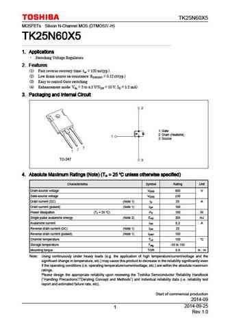
TK25N60X5 MOSFETs Silicon N-Channel MOS (DTMOS -H) TK25N60X5 TK25N60X5 TK25N60X5 TK25N60X5 1. Applications 1. Applications 1. Applications 1. Applications Switching Voltage Regulators 2. Features 2. Features 2. Features 2. Features (1) Fast reverse recovery time trr = 120 ns(typ.) (2) Low drain-source on-resistance RDS(ON) = 0.12 (typ.) (3) Easy to control Gate switc
tk25n60x.pdf
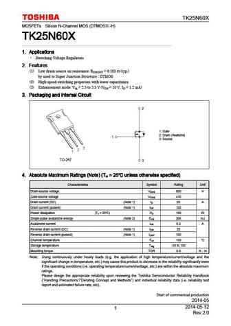
TK25N60X MOSFETs Silicon N-Channel MOS (DTMOS -H) TK25N60X TK25N60X TK25N60X TK25N60X 1. Applications 1. Applications 1. Applications 1. Applications Switching Voltage Regulators 2. Features 2. Features 2. Features 2. Features (1) Low drain-source on-resistance RDS(ON) = 0.105 (typ.) by used to Super Junction Structure DTMOS (2) High-speed switching properties wit
rej03g1118 h5n6001pds.pdf
To our customers, Old Company Name in Catalogs and Other Documents On April 1st, 2010, NEC Electronics Corporation merged with Renesas Technology Corporation, and Renesas Electronics Corporation took over all the business of both companies. Therefore, although the old company name remains in this document, it is a valid Renesas Electronics document. We appreciate your understanding.
fqp5n60c fqpf5n60c fqpf5n60cydtu.pdf
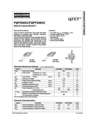
TM QFET FQP5N60C/FQPF5N60C 600V N-Channel MOSFET General Description Features These N-Channel enhancement mode power field effect 4.5A, 600V, RDS(on) = 2.5 @VGS = 10 V transistors are produced using Fairchild s proprietary, Low gate charge ( typical 15 nC) planar stripe, DMOS technology. Low Crss ( typical 6.5 pF) This advanced technology has been especially tailored t
fdd5n60nz.pdf
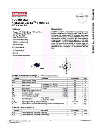
November 2013 FDD5N60NZ N-Channel UniFETTM II MOSFET 600 V, 4.0 A, 2 Features Description RDS(on) = 1.65 (Typ.) @ VGS = 10 V, ID = 2.0 A UniFETTM II MOSFET is Fairchild Semiconductor s high voltage MOSFET family based on advanced planar stripe and DMOS Low Gate Charge (Typ. 10 nC) technology. This advanced MOSFET family has the smallest Low Crss (Typ. 5 pF) on-stat
fqb5n60ctm fqb5n60c fqi5n60c fqi5n60ctu.pdf
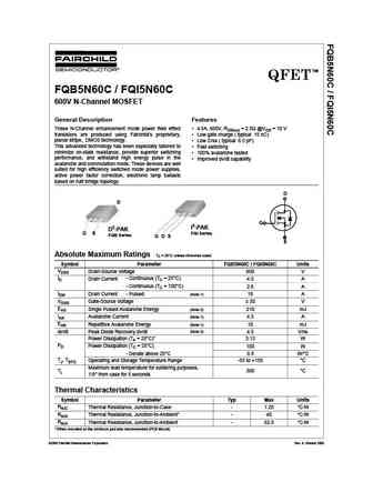
TM QFET FQB5N60C / FQI5N60C 600V N-Channel MOSFET General Description Features These N-Channel enhancement mode power field effect 4.5A, 600V, RDS(on) = 2.5 @VGS = 10 V transistors are produced using Fairchild s proprietary, Low gate charge ( typical 15 nC) planar stripe, DMOS technology. Low Crss ( typical 6.5 pF) This advanced technology has been especially tailored
fcd5n60tm ws.pdf
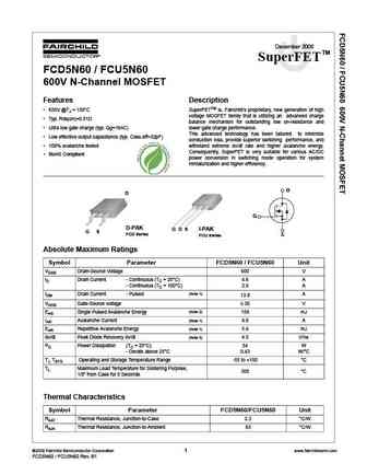
December 2008 TM SuperFET FCD5N60 / FCU5N60 600V N-Channel MOSFET Features Description 650V @TJ = 150 C SuperFETTM is, Fairchild s proprietary, new generation of high voltage MOSFET family that is utilizing an advanced charge Typ. Rds(on)=0.81 balance mechanism for outstanding low on-resistance and Ultra low gate charge (typ. Qg=16nC) lower gate charge performanc
fgh75n60uf.pdf
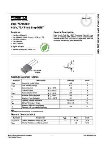
April 2009 FGH75N60UF tm 600V, 75A Field Stop IGBT Features General Description High Current Capability Using Novel Field Stop IGBT Technology, Fairchild s new series of Field Stop IGBTs offer the optimum performance for Low Saturation Voltage VCE(sat) =1.9V @ IC = 75A Induction Heating, UPS, SMPS and PFC applications where low High Input Impedance conduction and switch
fcd5n60 fcu5n60.pdf

December 2008 TM SuperFET FCD5N60 / FCU5N60 600V N-Channel MOSFET Features Description 650V @TJ = 150 C SuperFETTM is, Fairchild s proprietary, new generation of high voltage MOSFET family that is utilizing an advanced charge Typ. Rds(on)=0.81 balance mechanism for outstanding low on-resistance and Ultra low gate charge (typ. Qg=16nC) lower gate charge performanc
fqb5n60 fqi5n60.pdf
April 2000 TM QFET QFET QFET QFET FQB5N60 / FQI5N60 600V N-Channel MOSFET General Description Features These N-Channel enhancement mode power field effect 5.0A, 600V, RDS(on) = 2.0 @VGS = 10 V transistors are produced using Fairchild s proprietary, Low gate charge ( typical 16 nC) planar stripe, DMOS technology. Low Crss ( typical 9.0 pF) This advanced technology h
fcp25n60n f102.pdf
March 2013 FCP25N60N_F102 N-Channel SupreMOS MOSFET 600 V, 25 A, 125 m Features Description RDS(on) = 107 m (Typ.)@ VGS = 10 V, ID = 12.5 A The SupreMOS MOSFET is Fairchild Semiconductor s next- generation of high voltage super-junction (SJ) technology Ultra Low Gate Charge (Typ. Qg = 57 nC) employing a deep trench filling process that differentiate it from
fch25n60n.pdf
January 2011 SupreMOS FCH25N60N tm N-Channel MOSFET 600V, 25A, 0.126 Features Description RDS(on) = 0.108 ( Typ.) at VGS = 10V, ID = 12.5A The SupreMOS MOSFET, Fairchild s next generation of high voltage super-junction MOSFETs, employs a deep trench filling Ultra Low Gate Charge ( Typ. Qg = 57nC) process that differentiates it from preceding multi-epi based tech- n
fci25n60n.pdf
November 2013 FCI25N60N N-Channel SupreMOS MOSFET 600 V, 25 A, 125 m Features Description The SupreMOS MOSFET is Fairchild Semiconductor s next RDS(on) = 107 m (Typ.) @ VGS = 10 V, ID = 12.5 A generation of high voltage super-junction (SJ) technology Ultra Low Gate Charge (Typ. Qg = 57 nC) employing a deep trench filling process that differentiates it from Low Ef
fdp5n60nz fdpf5n60nz.pdf
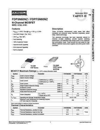
November 2010 TM UniFET-II FDP5N60NZ / FDPF5N60NZ N-Channel MOSFET 600V, 4.5A, 2.0 Features Description RDS(on) = 1.65 ( Typ.)@ VGS = 10V, ID = 2.25A These N-Channel enhancement mode power field effect transistors are produced using Fairchild s proprietary, planar Low Gate Charge ( Typ. 10nC) stripe, DMOS technology. Low Crss ( Typ. 5pF) This advanced techno
fdd5n60nztm.pdf
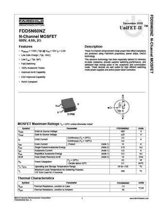
December 2010 TM UniFET-II FDD5N60NZ N-Channel MOSFET 600V, 4.0A, 2 Features Description RDS(on) = 1.65 ( Typ.)@ VGS = 10V, ID = 2.0A These N-Channel enhancement mode power field effect transistors are produced using Fairchild s proprietary, planar stripe, DMOS Low Gate Charge ( Typ. 10nC) technology. Low Crss ( Typ. 5pF) This advance technology has been e
fqb5n60tm.pdf

April 2000 TM QFET QFET QFET QFET FQB5N60 / FQI5N60 600V N-Channel MOSFET General Description Features These N-Channel enhancement mode power field effect 5.0A, 600V, RDS(on) = 2.0 @VGS = 10 V transistors are produced using Fairchild s proprietary, Low gate charge ( typical 16 nC) planar stripe, DMOS technology. Low Crss ( typical 9.0 pF) This advanced technology h
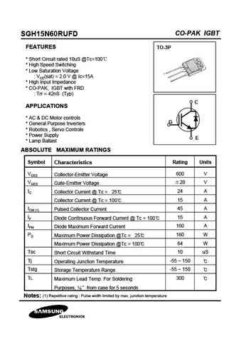
sgh15n60rufd.pdf
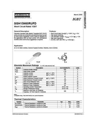
March 2000 IGBT SGH15N60RUFD Short Circuit Rated IGBT General Description Features Fairchild's Insulated Gate Bipolar Transistor(IGBT) RUFD Short Circuit rated 10us @ TC = 100 C, VGE = 15V series provides low conduction and switching losses as well High Speed Switching as short circuit ruggedness. RUFD series is designed for Low Saturation Voltage VCE(sat) = 2.2 V @ IC =
fcu5n60.pdf
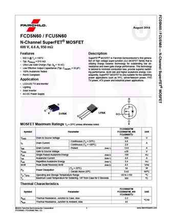
August 2014 FCD5N60 / FCU5N60 N-Channel SuperFET MOSFET 600 V, 4.6 A, 950 m Features Description 650 V @ TJ = 150 C SuperFET MOSFET is Fairchild Semiconductor s first genera- tion of high voltage super-junction (SJ) MOSFET family that is Typ. RDS(on) = 810 m utilizing charge balance technology for outstanding low on- Ultra Low Gate Charge (Typ. Qg = 16 nC) resis
fgp5n60ls.pdf
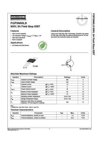
February 2010 FGP5N60LS tm 600V, 5A Field Stop IGBT Features General Description High Current Capability Using novel Field Stop IGBT Technology, Fairchild s new series of Field Stop IGBTs offer the optimum performance for HID bal- Low Saturation Voltage VCE(sat) =1.7V @ IC = 5A last where low conduction losses are essential. High Input Impedance RoHS Compliant Appl
fqpf5n60c.pdf
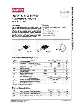
December 2013 FQP5N60C / FQPF5N60C N-Channel QFET MOSFET 600 V, 4.5 A, 2.5 Description Features This N-Channel enhancement mode power MOSFET is 4.5 A, 600 V, RDS(on) = 2.5 (Max.) @ VGS = 10 V, produced using Fairchild Semiconductor s proprietary planar ID = 2.25 A stripe and DMOS technology. This advanced MOSFET Low Gate Charge (Typ. 15 nC) technology has been
fch35n60.pdf
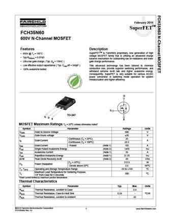
February 2010 SuperFETTM FCH35N60 600V N-Channel MOSFET Features Description SuperFETTM is Farichild s proprietary, new generation of high 650V @ TJ = 150 C voltage MOSFET family that is utilizing an advanced charge Typ.RDS(on) = 0.079 balance mechanism for outstanding low on-resistance and lower Ultra low gate charge ( Typ. Qg = 139nC ) gate charge performance.
fcp25n60n.pdf
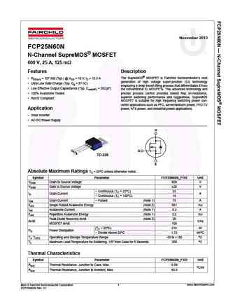
November 2013 FCP25N60N N-Channel SupreMOS MOSFET 600 V, 25 A, 125 m Features Description The SupreMOS MOSFET is Fairchild Semiconductor s next RDS(on) = 107 m (Typ.) @ VGS = 10 V, ID = 12.5 A generation of high voltage super-junction (SJ) technology Ultra Low Gate Charge (Typ. Qg = 57 nC) employing a deep trench filling process that differentiates it from Low Ef
fci25n60n f102.pdf
June 2010 TM SupreMOS FCI25N60N_F102 tm N-Channel MOSFET 600V, 25A, 0.125 Features Description RDS(on) = 0.107 ( Typ.)@ VGS = 10V, ID = 12.5A The SupreMOS MOSFET, Fairchild s next generation of high voltage super-junction MOSFETs, employs a deep trench filling Ultra Low Gate Charge ( Typ. Qg = 57nC) process that differentiates it from preceding multi-epi based tech-
fca35n60.pdf
March 2009 SuperFETTM FCA35N60 600V N-Channel MOSFET Features Description SuperFETTM is Farichild s proprietary, new generation of high 650V @ TJ = 150 C voltage MOSFET family that is utilizing an advanced charge bal- Typ.RDS(on) = 0.079 ance mechanism for outstanding low on-resistance and lower Ultra low gate charge ( Typ. Qg = 139nC ) gate charge performance.
fqpf5n60.pdf
TM QFET FQPF5N60 600V N-Channel MOSFET General Description Features These N-Channel enhancement mode power field effect 2.8A, 600V, RDS(on) = 2.0 @VGS = 10 V transistors are produced using Fairchild s proprietary, Low gate charge ( typical 16 nC) planar stripe, DMOS technology. Low Crss ( typical 9.0 pF) This advanced technology has been especially tailored to Fas
fqd5n60ctf fqd5n60ctm fqd5n60c fqu5n60c fqu5n60ctu.pdf
October 2008 QFET FQD5N60C / FQU5N60C 600V N-Channel MOSFET General Description Features These N-Channel enhancement mode power field effect 2.8A, 600V, RDS(on) = 2.5 @VGS = 10 V transistors are produced using Fairchild s proprietary, Low gate charge ( typical 15 nC) planar stripe, DMOS technology. Low Crss ( typical 6.5 pF) This advanced technology has been especia
sgs5n60rufd.pdf
April 2001 IGBT SGS5N60RUFD Short Circuit Rated IGBT General Description Features Fairchild's RUFD series of Insulated Gate Bipolar Short circuit rated 10us @ TC = 100 C, VGE = 15V Transistors (IGBTs) provide low conduction and switching High speed switching losses as well as short circuit ruggedness. The RUFD Low saturation voltage VCE(sat) = 2.2 V @ IC = 5A series is
sgw5n60ruf.pdf
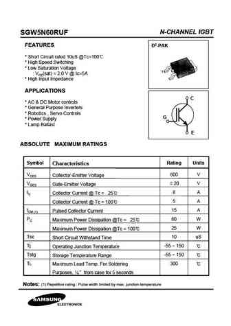
N-CHANNEL IGBT SGW5N60RUF FEATURES D2-PAK * Short Circuit rated 10uS @Tc=100 * High Speed Switching * Low Saturation Voltage VCE(sat) = 2.0 V @ Ic=5A * High Input Impedance APPLICATIONS C * AC & DC Motor controls * General Purpose Inverters * Robotics , Servo Controls G * Power Supply * Lamp Ballast E ABSOLUTE MAXIMUM RATINGS Symbol Rating Units Characteristics VCES
sgh15n60rufd.pdf
CO-PAK IGBT SGH15N60RUFD FEATURES TO-3P * Short Circuit rated 10uS @Tc=100 * High Speed Switching * Low Saturation Voltage VCE(sat) = 2.0 V @ Ic=15A * High Input Impedance * CO-PAK, IGBT with FRD Trr = 42nS (Typ) C APPLICATIONS * AC & DC Motor controls G * General Purpose Inverters * Robotics , Servo Controls * Power Supply E * Lamp Ballast ABSOLUTE MAXIMUM RATINGS
sgp5n60rufd.pdf
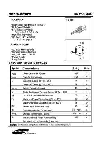
CO-PAK IGBT SGP5N60RUFD FEATURES TO-220 * Short Circuit rated 10uS @Tc=100 * High Speed Switching * Low Saturation Voltage VCE(sat) = 2.0 V @ Ic=5A * High Input Impedance * CO-PAK, IGBT with FRD Trr = 37nS (Typ.) C APPLICATIONS * AC & DC Motor controls G * General Purpose Inverters * Robotics , Servo Controls * Power Supply E * Lamp Ballast ABSOLUTE MAXIMUM RATINGS
sgp5n60ruf.pdf
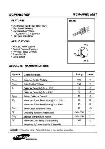
N-CHANNEL IGBT SGP5N60RUF FEATURES TO-220 * Short Circuit rated 10uS @Tc=100 * High Speed Switching * Low Saturation Voltage VCE(sat) = 2.0 V @ Ic=5A * High Input Impedance APPLICATIONS C * AC & DC Motor controls * General Purpose Inverters * Robotics , Servo Controls G * Power Supply * Lamp Ballast E ABSOLUTE MAXIMUM RATINGS Symbol Rating Units Characteristics VCES
sgw5n60rufd.pdf
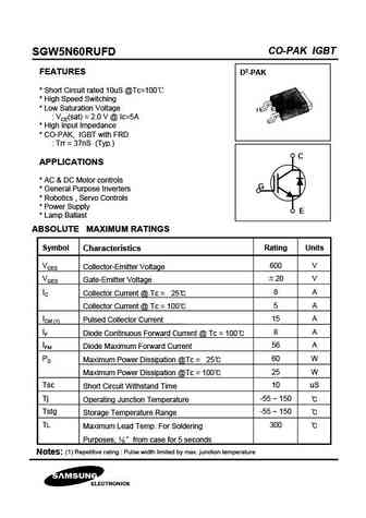
CO-PAK IGBT SGW5N60RUFD FEATURES D2-PAK * Short Circuit rated 10uS @Tc=100 * High Speed Switching * Low Saturation Voltage VCE(sat) = 2.0 V @ Ic=5A * High Input Impedance * CO-PAK, IGBT with FRD Trr = 37nS (Typ.) C APPLICATIONS * AC & DC Motor controls G * General Purpose Inverters * Robotics , Servo Controls * Power Supply E * Lamp Ballast ABSOLUTE MAXIMUM RATINGS
sgp15n60ruf.pdf
N-CHANNEL IGBT SGP15N60RUF FEATURES TO-220 * Short Circuit rated 10uS @Tc=100 * High Speed Switching * Low Saturation Voltage VCE(sat) = 2.0 V @ Ic=15A * High Input Impedance APPLICATIONS C * AC & DC Motor controls * General Purpose Inverters G * Robotics , Servo Controls * Power Supply * Lamp Ballast E ABSOLUTE MAXIMUM RATINGS Symbol Rating Units Characteristics VCE
rdx045n60fu6.pdf
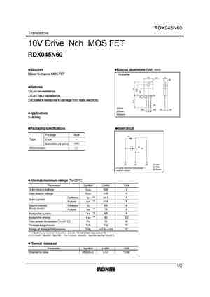
RDX045N60 Transistors 10V Drive Nch MOS FET RDX045N60 Structure External dimensions (Unit mm) Silicon N-channel MOS FET TO-220FM 10.0 3.2 4.5 2.8 Features 1) Low on-resistance. 1.2 2) Low input capacitance. 1.3 3) Excellent resistance to damage from static electricity. 0.8 (1)Gate 2.54 2.54 0.75 2.6 (2)Drain (1) (2) (3) Applications (3)Source Switching P
siha15n60e.pdf
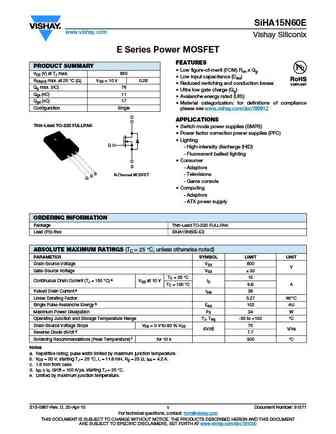
SiHA15N60E www.vishay.com Vishay Siliconix E Series Power MOSFET FEATURES PRODUCT SUMMARY Low figure-of-merit (FOM) Ron x Qg VDS (V) at TJ max. 650 Low input capacitance (Ciss) RDS(on) max. at 25 C ( ) VGS = 10 V 0.28 Reduced switching and conduction losses Qg max. (nC) 76 Ultra low gate charge (Qg) Qgs (nC) 11 Avalanche energy rated (UIS) Qgd (nC) 17
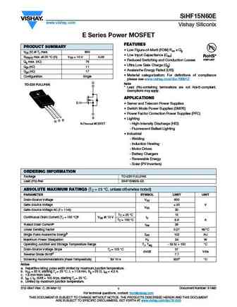
sihp15n60e.pdf
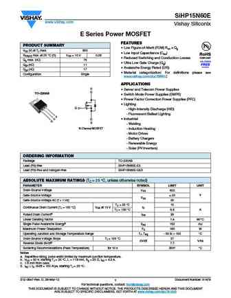
SiHP15N60E www.vishay.com Vishay Siliconix E Series Power MOSFET FEATURES PRODUCT SUMMARY Low Figure-of-Merit (FOM) Ron x Qg VDS (V) at TJ max. 650 Low Input Capacitance (Ciss) RDS(on) max. at 25 C ( ) VGS = 10 V 0.28 Reduced Switching and Conduction Losses Qg max. (nC) 76 Ultra Low Gate Charge (Qg) Qgs (nC) 11 Avalanche Energy Rated (UIS) Qgd (nC) 17
irfp15n60lpbf.pdf
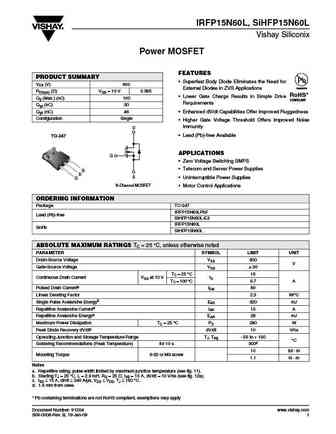
IRFP15N60L, SiHFP15N60L Vishay Siliconix Power MOSFET FEATURES PRODUCT SUMMARY Superfast Body Diode Eliminates the Need for VDS (V) 600 Available External Diodes in ZVS Applications RDS(on) ( )VGS = 10 V 0.385 RoHS* Lower Gate Charge Results in Simple Drive Qg (Max.) (nC) 100 COMPLIANT Requirements Qgs (nC) 30 Qgd (nC) 46 Enhanced dV/dt Capabilities Offer Improved
sihb15n60e.pdf
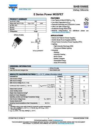
SiHB15N60E www.vishay.com Vishay Siliconix E Series Power MOSFET FEATURES PRODUCT SUMMARY Low Figure-of-Merit (FOM) Ron x Qg VDS (V) at TJ max. 650 Low Input Capacitance (Ciss) RDS(on) max. at 25 C ( ) VGS = 10 V 0.28 Reduced Switching and Conduction Losses Qg max. (nC) 76 Ultra Low Gate Charge (Qg) Qgs (nC) 11 Avalanche Energy Rated (UIS) Qgd (nC) 17
sihp25n60efl.pdf
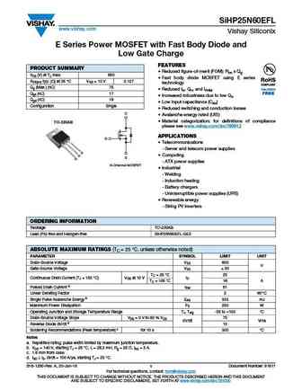
SiHP25N60EFL www.vishay.com Vishay Siliconix E Series Power MOSFET with Fast Body Diode and Low Gate Charge FEATURES PRODUCT SUMMARY Reduced figure-of-merit (FOM) Ron x Qg VDS (V) at TJ max. 650 Fast body diode MOSFET using E series RDS(on) typ. ( ) at 25 C VGS = 10 V 0.127 technology Qg (Max.) (nC) 75 Reduced trr, Qrr, and IRRM Qgs (nC) 17 Increased robust
sihf15n60e.pdf
SiHF15N60E www.vishay.com Vishay Siliconix E Series Power MOSFET FEATURES PRODUCT SUMMARY Low Figure-of-Merit (FOM) Ron x Qg VDS (V) at TJ max. 650 Low Input Capacitance (Ciss) RDS(on) max. at 25 C ( ) VGS = 10 V 0.28 Reduced Switching and Conduction Losses Qg max. (nC) 76 Ultra Low Gate Charge (Qg) Qgs (nC) 11 Avalanche Energy Rated (UIS) Qgd (nC) 17
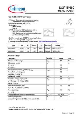
sgb15n60.pdf

SGB15N60 Fast IGBT in NPT-technology C 75% lower Eoff compared to previous generation combined with low conduction losses Short circuit withstand time 10 s G E Designed for - Motor controls - Inverter NPT-Technology for 600V applications offers - very tight parameter distribution - high ruggedness, temperature stable behaviour PG-TO-263-3-2 -
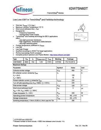
igw75n60h3.pdf
IGBT High speed IGBT in Trench and Fieldstop technology IGW75N60H3 600V high speed switching series third generation Data sheet Industrial & Multimarket IGW75N60H3 High speed switching series third generation High speed IGBT in Trench and Fieldstop technology Features C TRENCHSTOPTM technology offering very low V CEsat low EMI maximum junction temperature 175 C
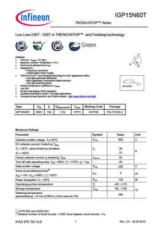
igb15n60t.pdf
IGB15N60T TRENCHSTOP Series q Low Loss IGBT IGBT in TRENCHSTOP and Fieldstop technology C G E Features Very low VCE(sat) 1.5V (typ.) Maximum Junction Temperature 175 C Short circuit withstand time 5 s Designed for frequency inverters for washing machines, fans, pumps and vacuum cleaners TRENCHSTOP technology for 600V applications offers
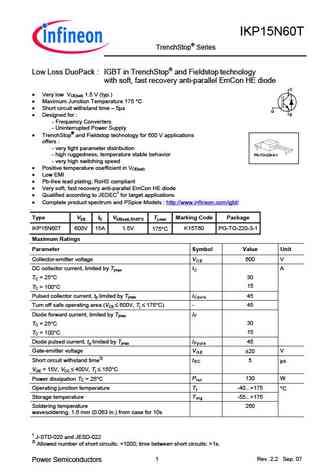
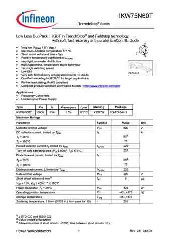
ikp15n60t.pdf
IKP15N60T TRENCHSTOP Series q Low Loss DuoPack IGBT in TRENCHSTOP and Fieldstop technology with soft, fast recovery anti-parallel Emitter Controlled HE diode C Features Very low VCE(sat) 1.5V (typ.) Maximum Junction Temperature 175 C Short circuit withstand time 5 s G Designed for E - Frequency Converters - Uninterrupted Power Supply
sgw15n60.pdf

SGP15N60 SGW15N60 Fast IGBT in NPT-technology C 75% lower Eoff compared to previous generation combined with low conduction losses Short circuit withstand time 10 s G E Designed for - Motor controls - Inverter NPT-Technology for 600V applications offers - very tight parameter distribution - high ruggedness, temperature stable behaviour - paral
iku15n60r.pdf
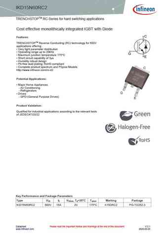
IGBT IGBT with integrated diode in packages offering space saving advantage IKD15N60R, IKU15N60R 600V TRENCHSTOPTM RC-Series for hard switching applications Datasheet Industrial & Multimarket IKD15N60R, IKU15N60R TRENCHSTOPTM RC-Series for hard switching applications IGBT with integrated diode in packages offering space saving advantage C Features TRENCHSTOPTM Reverse Conducting (R
sgp15n60.pdf

SGP15N60 SGW15N60 Fast IGBT in NPT-technology C 75% lower Eoff compared to previous generation combined with low conduction losses Short circuit withstand time 10 s G E Designed for - Motor controls - Inverter NPT-Technology for 600V applications offers - very tight parameter distribution - high ruggedness, temperature stable behaviour - paral
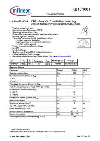
ikb15n60t.pdf
IKB15N60T TRENCHSTOP Series q Low Loss DuoPack IGBT in TRENCHSTOP and Fieldstop technology with soft, fast recovery anti-parallel Emitter Controlled HE diode C Features Very low VCE(sat) 1.5V (typ.) Maximum Junction Temperature 175 C Short circuit withstand time 5 s G Designed for frequency inverters for washing machines, fans, pumps and vacuum
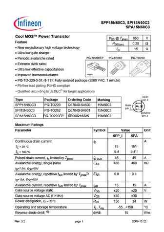
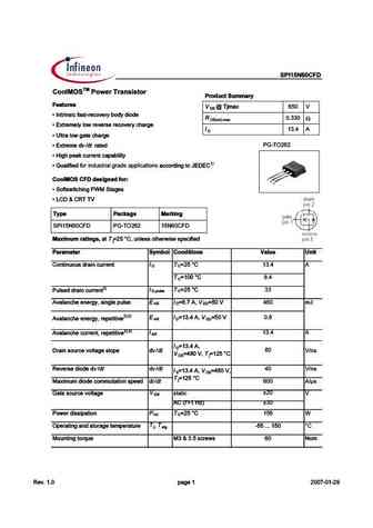
spp15n60c3 spi15n60c3 spa15n60c3.pdf
SPP15N60C3, SPI15N60C3 SPA15N60C3 Cool MOS Power Transistor VDS @ Tjmax 650 V Feature RDS(on) 0.28 New revolutionary high voltage technology ID 15 A Ultra low gate charge PG-TO220FP PG-TO262 PG-TO220 Periodic avalanche rated Extreme dv/dt rated 3 Ultra low effective capacitances 2 1 P-TO220-3-31 Improved transconductance PG-TO-220-3-31;-3-111
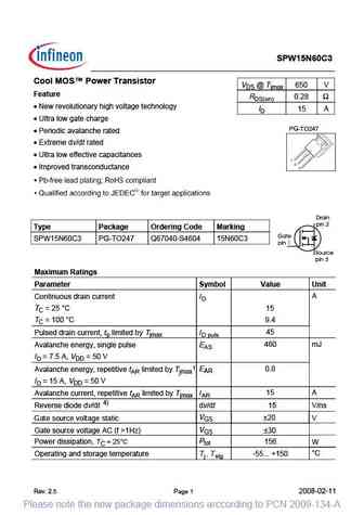
igw75n60t.pdf
IGW75N60T TRENCHSTOP Series q Low Loss IGBT IGBT in TRENCHSTOP and Fieldstop technology C Features Very low VCE(sat) 1.5V (typ.) Maximum Junction Temperature 175 C Short circuit withstand time 5 s G Designed for E - Frequency Converters - Uninterrupted Power Supply TRENCHSTOP and Fieldstop technology for 600V applications offers
igp15n60trev2 2g.pdf
IGP15N60T TrenchStop Series q Low Loss IGBT in TrenchStop and Fieldstop technology C Very low VCE(sat) 1.5 V (typ.) Maximum Junction Temperature 175 C Short circuit withstand time 5 s G Designed for E - Frequency Converters - Uninterrupted Power Supply TrenchStop and Fieldstop technology for 600 V applications offers - very tight p
spp15n60cfd.pdf
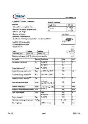
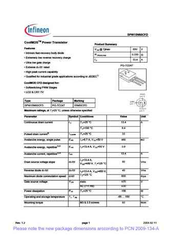
SPP15N60CFD CoolMOSTM Power Transistor Product Summary Features V @ Tjmax 650 V DS Intrinsic fast-recovery body diode R 0.330 DS(on),max Extremely low reverse recovery charge I 13.4 A D Ultra low gate charge Extreme dv /dt rated PG-TO220 High peak current capability Qualified for industrial grade applications according to JEDEC1) CoolMOS CFD designed fo
ika15n60t.pdf
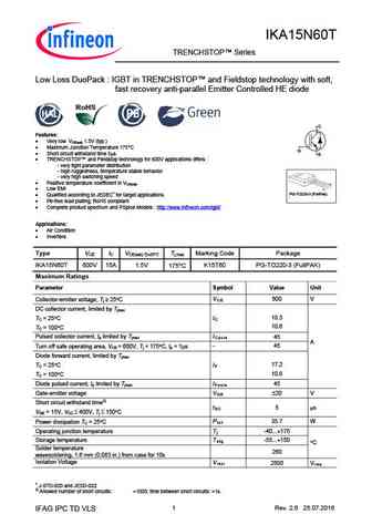
IKA15N60T TRENCHSTOP Series q Low Loss DuoPack IGBT in TRENCHSTOP and Fieldstop technology with soft, fast recovery anti-parallel Emitter Controlled HE diode C Features Very low VCE(sat) 1.5V (typ.) Maximum Junction Temperature 175 C G Short circuit withstand time 5 s E TRENCHSTOP and Fieldstop technology for 600V applications offers - ve
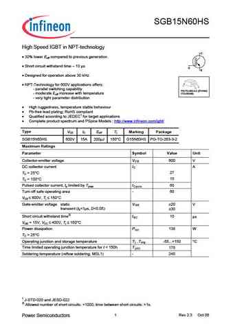
sgb15n60hs.pdf
SGB15N60HS ^ High Speed IGBT in NPT-technology C 30% lower Eoff compared to previous generation Short circuit withstand time 10 s G E Designed for operation above 30 kHz NPT-Technology for 600V applications offers - parallel switching capability PG-TO-263-3-2 (D -PAK) - moderate Eoff increase with temperature (TO-263AB) - very tight parameter distri
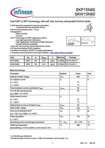
skp15n60.pdf

SKP15N60 SKW15N60 Fast IGBT in NPT-technology with soft, fast recovery anti-parallel EmCon diode C 75% lower Eoff compared to previous generation combined with low conduction losses Short circuit withstand time 10 s G E Designed for - Motor controls - Inverter NPT-Technology for 600V applications offers - very tight parameter distribution - high
skw15n60.pdf

SKP15N60 SKW15N60 Fast IGBT in NPT-technology with soft, fast recovery anti-parallel EmCon diode C 75% lower Eoff compared to previous generation combined with low conduction losses Short circuit withstand time 10 s G E Designed for - Motor controls - Inverter NPT-Technology for 600V applications offers - very tight parameter distribution - high
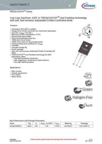
aikw75n60ct.pdf
AIKW75N60CT TRENCHSTOPTM Series Low Loss DuoPack IGBT in TRENCHSTOPTM and Fieldstop technology with soft, fast recovery antiparallel Emitter Controlled diode C Features Automotive AEC-Q101 qualified Designed for DC/AC converters for Automotive Application Very low V 1.5V (typ.) CE(sat) Maximum junction temperature 175 C G Dynamically stress tested E Shor
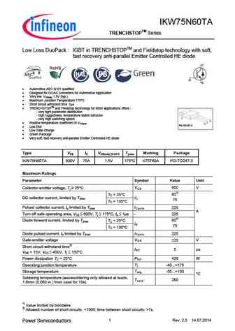
ikw75n60t.pdf
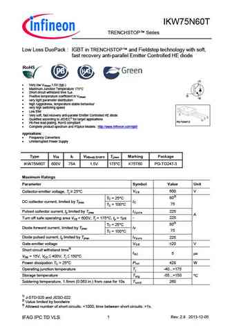
IKW75N60T TRENCHSTOP Series q Low Loss DuoPack IGBT in TRENCHSTOP and Fieldstop technology with soft, fast recovery anti-parallel Emitter Controlled HE diode C Very low VCE(sat) 1.5V (typ.) Maximum Junction Temperature 175 C Short circuit withstand time 5 s G Positive temperature coefficient in VCE(sat) E very tight parameter distribution high rugg
ikb15n60trev2 5g.pdf
IKB15N60T TrenchStop Series q Low Loss DuoPack IGBT in TrenchStop and Fieldstop technology with soft, fast recovery anti-parallel EmCon 3 diode C Very low VCE(sat) 1.5 V (typ.) Maximum Junction Temperature 175 C Short circuit withstand time 5 s G E Designed for frequency inverters for washing machines, fans, pumps and vacuum cleaners Trench
spw15n60cfd.pdf
SPW15N60CFD TM C IMOSTM # A0D9 R 0. 0 DS(on) max V "MIG B AN ADL G K GH G 8DK GN 8=6G;> 9 688DG9>CC
skp15n60 skw15n60.pdf
SKP15N60 SKW15N60 Fast IGBT in NPT-technology with soft, fast recovery anti-parallel EmCon diode C 75% lower Eoff compared to previous generation combined with low conduction losses Short circuit withstand time 10 s G E Designed for - Motor controls - Inverter NPT-Technology for 600V applications offers - very tight parameter distribution - high
spa15n60cfd.pdf
SPA15N60CFD CoolMOSTM Power Transistor Product Summary Features V @ Tjmax 650 V DS Intrinsic fast-recovery body diode R 0.330 DS(on),max Extremely low reverse recovery charge I 13.4 A D Ultra low gate charge Extreme dv /dt rated PG-TO220FP High peak current capability Qualified according to JEDEC1) for target applications CoolMOS CFD designed for
skb15n60.pdf
SKB15N60 Fast IGBT in NPT-technology with soft, fast recovery anti-parallel Emitter Controlled Diode C 75% lower Eoff compared to previous generation combined with low conduction losses Short circuit withstand time 10 s G E Designed for frequency inverters for washing machines, fans, pumps and vacuum cleaners NPT-Technology for 600V applications offers - very
igb15n60trev2 4g.pdf
IGB15N60T TrenchStop Series q Low Loss IGBT in TrenchStop technology C Very low VCE(sat) 1.5 V (typ.) Maximum Junction Temperature 175 C Short circuit withstand time 5 s G Designed for frequency inverters for washing machines, fans, E pumps and vacuum cleaners TrenchStop technology for 600 V applications offers - very tight parameter distr
ika15n60trev2 3g.pdf
IKA15N60T TrenchStop Series q Low Loss DuoPack IGBT in TrenchStop and Fieldstop technology with soft, fast recovery anti-parallel EmCon HE diode C Very low VCE(sat) 1.5 V (typ.) Maximum Junction Temperature 175 C Short circuit withstand time 5 s G E TrenchStop and Fieldstop technology for 600 V applications offers - very tight parameter di
ikd15n60rc2.pdf
IKD15N60RC2 TRENCHSTOPTM RC-Series for hard switching applications Cost effective monolithically integrated IGBT with Diode C Features TRENCHSTOPTM Reverse Conducting (RC) technology for 600V applications offering Very tight parameter distribution Operating range up to 20kHz G Maximum junction temperature 175 C E Short circuit capability of 3 s Humidity robus
sgb15n60hs .pdf

SGB15N60HS ^ High Speed IGBT in NPT-technology C 30% lower Eoff compared to previous generation Short circuit withstand time 10 s G E Designed for operation above 30 kHz NPT-Technology for 600V applications offers - parallel switching capability PG-TO-263-3-2 (D -PAK) - moderate Eoff increase with temperature (TO-263AB) - very tight parameter distri
ikd15n60rf.pdf

IGBT IGBT with integrated diode in packages offering space saving advantage IKD15N60RF TRENCHSTOPTM RC-Series for hard switching applications up to 30 kHz Data sheet Industrial Power Control IKD15N60RF TRENCHSTOPTM RC-Drives Fast Series IGBT with integrated diode in packages offering space saving advantage C Features TRENCHSTOPTM Reverse Conducting (RC) technology for 600V applica
ikd15n60ra.pdf
IGBT IGBT with integrated diode in packages offering space saving advantage IKD15N60RA 600V TRENCHSTOPTM RC-Series for hard switching applications Data sheet Industrial Power Control IKD15N60RA TRENCHSTOPTM RC-Series for hard switching applications IGBT with integrated diode in packages offering space saving advantage C Features TRENCHSTOPTM Reverse Conducting (RC) technology for 6
sgp15n60 sgw15n60g.pdf
SGP15N60 SGW15N60 Fast IGBT in NPT-technology C 75% lower Eoff compared to previous generation combined with low conduction losses Short circuit withstand time 10 s G E Designed for - Motor controls - Inverter NPT-Technology for 600V applications offers - very tight parameter distribution - high ruggedness, temperature stable behaviour - paral
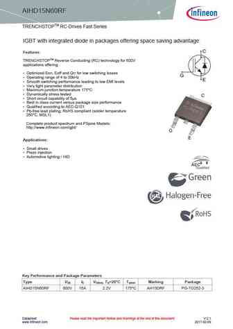
aihd15n60r.pdf
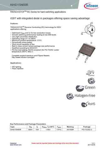
AIHD15N60R TRENCHSTOPTM RC-Series for hard switching applications IGBT with integrated diode in packages offering space saving advantage C Features TRENCHSTOPTM Reverse Conducting (RC) technology for 600V applications offering Optimised V and V for low conduction losses CEsat F G Smooth switching performance leading to low EMI levels E Very tight parameter distribution
skb15n60hs.pdf

SKB15N60HS High Speed IGBT in NPT-technology C 30% lower Eoff compared to previous generation Short circuit withstand time 10 s G E Designed for operation above 30 kHz NPT-Technology for 600V applications offers PG-TO263-3-2 - parallel switching capability - moderate Eoff increase with temperature - very tight parameter distribution High ruggedne
spp15n60c3 spi15n60c3 spa15n60c3 rev.3.2new.pdf
SPP15N60C3, SPI15N60C3 SPA15N60C3 Cool MOS Power Transistor VDS @ Tjmax 650 V Feature RDS(on) 0.28 New revolutionary high voltage technology ID 15 A Ultra low gate charge PG-TO220FP PG-TO262 PG-TO220 Periodic avalanche rated Extreme dv/dt rated 3 Ultra low effective capacitances 2 1 P-TO220-3-31 Improved transconductance PG-TO-220-3-31;-3-111
ikp15n60trev2 2g.pdf
IKP15N60T TrenchStop Series q Low Loss DuoPack IGBT in TrenchStop and Fieldstop technology with soft, fast recovery anti-parallel EmCon HE diode C Very low VCE(sat) 1.5 V (typ.) Maximum Junction Temperature 175 C Short circuit withstand time 5 s G E Designed for - Frequency Converters - Uninterrupted Power Supply TrenchStop and Fiel
ikfw75n60et.pdf
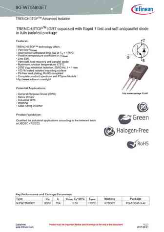
IKFW75N60ET TRENCHSTOPTM Advanced Isolation TRENCHSTOPTM IGBT copacked with Rapid 1 fast and soft antiparallel diode in fully isolated package C Features TRENCHSTOP technology offers Very low V CE(sat) Short circuit withstand time 5 s at T = 175 C vj Positive temperature coefficient in V CE(sat) G Low EMI E Very soft, fast recovery anti-parallel diode
ikw75n60trev2 6g.pdf
IKW75N60T TrenchStop Series q Low Loss DuoPack IGBT in TrenchStop and Fieldstop technology with soft, fast recovery anti-parallel EmCon HE diode C Very low VCE(sat) 1.5 V (typ.) Maximum Junction Temperature 175 C G Short circuit withstand time 5 s E Positive temperature coefficient in VCE(sat) very tight parameter distribution high rugg
ikd15n60r.pdf
IGBT IGBT with integrated diode in packages offering space saving advantage IKD15N60R 600V TRENCHSTOPTM RC-Series for hard switching applications Data sheet Industrial Power Control IKD15N60R TRENCHSTOPTM RC-Series for hard switching applications IGBT with integrated diode in packages offering space saving advantage C Features TRENCHSTOPTM Reverse Conducting (RC) technology for 600
spw35n60cfd.pdf
SPW35N60CFD TM C IMOSTM $;B1= '=- >5>?;= $=;0@/? &@99-=D Features D D U * 9K F9JC@IH=CB5FM
ikw75n60h3.pdf

IGBT High speed DuoPack IGBT in Trench and Fieldstop technology with soft, fast recovery anti-parallel diode IKW75N60H3 600V high speed switching series third generation Data sheet Industrial & Multimarket IKW75N60H3 High speed switching series third generation High speed IGBT in Trench and Fieldstop technology C Features TRENCHSTOPTM technology offering very lo
spw35n60c3.pdf
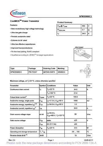
SPW35N60C3 CoolMOSTM Power Transistor Product Summary Features V @ T 650 V DS j,max New revolutionary high voltage technology R 0.1 DS(on),max Ultra low gate charge I 34.6 A D Periodic avalanche rated Extreme dv /dt rated Ultra low effective capacitances PG-TO247 Improved transconductance Type Package Ordering Code Marking SPW35N60C3 PG-TO247 Q6704
sgb15n60g.pdf
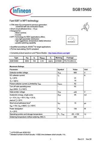
SGB15N60 Fast IGBT in NPT-technology C 75% lower Eoff compared to previous generation combined with low conduction losses Short circuit withstand time 10 s G E Designed for - Motor controls - Inverter NPT-Technology for 600V applications offers - very tight parameter distribution - high ruggedness, temperature stable behaviour PG-TO-263-3-2 -
skb15n60hsg.pdf
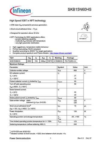
SKB15N60HS High Speed IGBT in NPT-technology C 30% lower Eoff compared to previous generation Short circuit withstand time 10 s G E Designed for operation above 30 kHz NPT-Technology for 600V applications offers PG-TO263-3-2 - parallel switching capability - moderate Eoff increase with temperature - very tight parameter distribution High ruggedne
skb15n60g.pdf
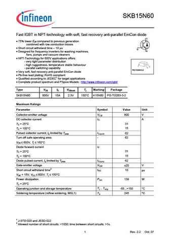
SKB15N60 Fast IGBT in NPT-technology with soft, fast recovery anti-parallel EmCon diode C 75% lower Eoff compared to previous generation combined with low conduction losses Short circuit withstand time 10 s G E Designed for frequency inverters for washing machines, fans, pumps and vacuum cleaners NPT-Technology for 600V applications offers - very tight
aihd15n60rf.pdf
AIHD15N60RF TRENCHSTOPTM RC-Drives Fast Series IGBT with integrated diode in packages offering space saving advantage C Features TRENCHSTOPTM Reverse Conducting (RC) technology for 600V applications offering Optimized Eon, Eoff and Qrr for low switching losses G Operating range of 4 to 30kHz E Smooth switching performance leading to low EMI levels Very tight paramet
spi15n60cfd b.pdf
SPI15N60CFD C IMOSTM $;B1= '=- >5>?;= $=;0@/? &@99-=D Features V 1?B6M 650 V !0 V &CIG>CH>8 ;6HI G 8DK GN 7D9N 9>D9 R 0. 0 DS(on) max V "MIG B AN ADL G K GH G 8DK GN 8=6G;> 9 for industrial grade applications 688DG9>C53 10 2;= V 0D;IHL>I8
igp15n60t.pdf
IGP15N60T TRENCHSTOP Series q Low Loss IGBT IGBT in TRENCHSTOP and Fieldstop technology C Features Very low VCE(sat) 1.5V (typ.) Maximum Junction Temperature 175 C G Short circuit withstand time 5 s E Designed for - Frequency Converters - Uninterrupted Power Supply TRENCHSTOP and Fieldstop technology for 600V applications offers
igw75n60t rev2 5g.pdf
IGW75N60T TrenchStop Series q Low Loss IGBT in TrenchStop and Fieldstop technology C Very low VCE(sat) 1.5 V (typ.) Maximum Junction Temperature 175 C Short circuit withstand time 5 s G Designed for E - Frequency Converters - Uninterrupted Power Supply TrenchStop and Fieldstop technology for 600 V applications offers PG-TO-247-3
ixkp35n60c5.pdf
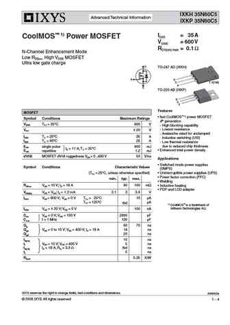
IXKH 35N60C5 Advanced Technical Information IXKP 35N60C5 ID25 = 35 A CoolMOS 1) Power MOSFET VDSS = 600 V RDS(on) max = 0.1 N-Channel Enhancement Mode Low RDSon, High VDSS MOSFET Ultra low gate charge D TO-247 AD (IXKH) G G D D(TAB) S S TO-220 AB (IXKP) G D S Features MOSFET fast CoolMOS 1) power MOSFET Symbol Conditions Maximum Ratings 4th generation V
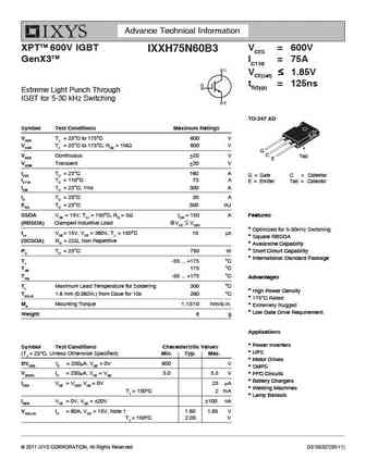
ixgb75n60bd1.pdf
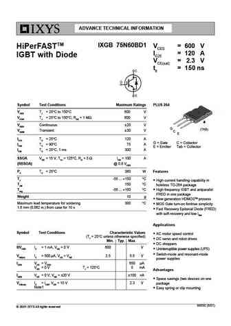
ADVANCE TECHNICAL INFORMATION IXGB 75N60BD1 VCES = 600 V HiPerFASTTM IC25 = 120 A IGBT with Diode VCE(sat) = 2.3 V tfi = 150 ns Symbol Test Conditions Maximum Ratings PLUS 264 VCES TJ = 25 C to 150 C 600 V VCGR TJ = 25 C to 150 C; RGE = 1 M 600 V VGES Continuous 20 V G (TAB) VGEM Transient 30 V C E IC25 TC = 25 C 120 A G = Gate C = Collector IC90 TC = 90 C75 A
ixdr35n60bd1.pdf
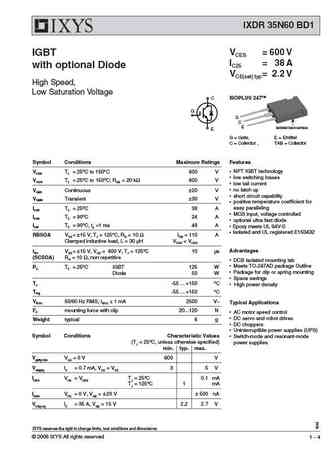
IXDR 35N60 BD1 VCES = 600 V IGBT IC25 = 38 A with optional Diode VCE(sat) typ= 2.2 V High Speed, Low Saturation Voltage C ISOPLUS 247TM G G C E Isolated back surface E G = Gate, E = Emitter C = Collector , TAB = Collector Symbol Conditions Maximum Ratings Features NPT IGBT technology VCES TJ = 25 C to 150 C 600 V low switching losses VCGR TJ = 25 C to 150 C;
ixta5n60p ixtp5n60p.pdf
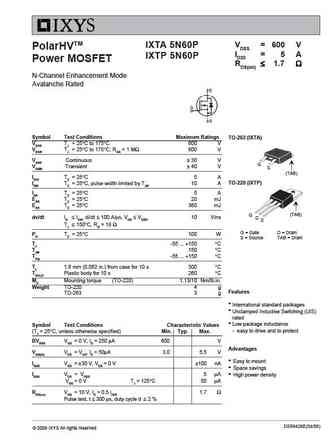
VDSS = 600 V IXTA 5N60P PolarHVTM ID25 = 5 A IXTP 5N60P Power MOSFET RDS(on) 1.7 N-Channel Enhancement Mode Avalanche Rated Symbol Test Conditions Maximum Ratings TO-263 (IXTA) VDSS TJ = 25 C to 175 C 600 V VDGR TJ = 25 C to 175 C; RGS = 1 M 600 V VGSS Continuous 30 V G VGSM Transient 40 V S (TAB) ID25 TC = 25 C5 A TO-220 (I
ixth15n60 ixtm15n60 ixth20n60 ixtm20n60.pdf
Downloaded from DatasheetLib.com - datasheet search engine Downloaded from DatasheetLib.com - datasheet search engine Downloaded from DatasheetLib.com - datasheet search engine Downloaded from DatasheetLib.com - datasheet search engine
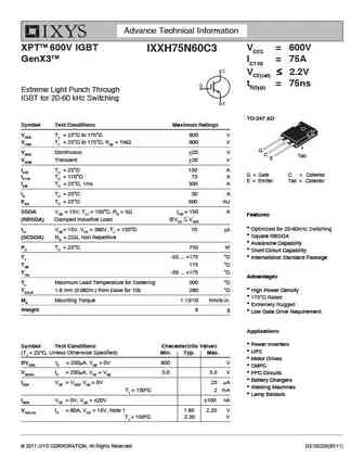
ixxh75n60b3.pdf
Advance Technical Information XPTTM 600V IGBT VCES = 600V IXXH75N60B3 GenX3TM IC110 = 75A VCE(sat) 1.85V tfi(typ) = 125ns Extreme Light Punch Through IGBT for 5-30 kHz Switching TO-247 AD Symbol Test Conditions Maximum Ratings VCES TJ = 25 C to 175 C 600 V VCGR TJ = 25 C to 175 C, RGE = 1M 600 V G C VGES Continuous 20 V Tab E VGEM Transient
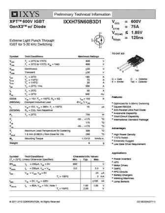
ixxh75n60c3d1.pdf
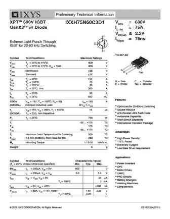
Preliminary Technical Information XPTTM 600V IGBT VCES = 600V IXXH75N60C3D1 GenX3TM w/ Diode IC110 = 75A VCE(sat) 2.2V tfi(typ) = 75ns Extreme Light Punch Through IGBT for 20-60 kHz Switching TO-247 AD Symbol Test Conditions Maximum Ratings VCES TJ = 25 C to 175 C 600 V VCGR TJ = 25 C to 175 C, RGE = 1M 600 V G VGES Continuous 20 V C Tab E V
ixdh35n60b.pdf
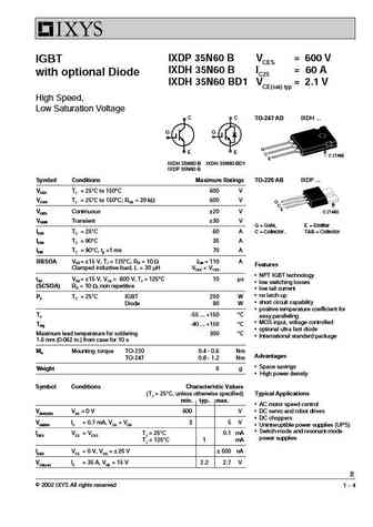
IXDP 35N60 B VCES = 600 V IGBT IXDH 35N60 B IC25 = 60 A with optional Diode IXDH 35N60 BD1 VCE(sat) typ = 2.1 V High Speed, Low Saturation Voltage C C TO-247 AD IXDH ... G G G E E C C (TAB) E IXDH 35N60 B IXDH 35N60 BD1 IXDP 35N60 B Symbol Conditions Maximum Ratings TO-220 AB IXDP ... VCES TJ = 25 C to 150 C 600 V VCGR TJ = 25 C to 150 C; RGE = 20 kW 600 V G C E VG
ixdp35n60b.pdf

IXDP 35N60 B VCES = 600 V IGBT IXDH 35N60 B IC25 = 60 A with optional Diode IXDH 35N60 BD1 VCE(sat) typ = 2.1 V High Speed, Low Saturation Voltage C C TO-247 AD IXDH ... G G G E E C C (TAB) E IXDH 35N60 B IXDH 35N60 BD1 IXDP 35N60 B Symbol Conditions Maximum Ratings TO-220 AB IXDP ... VCES TJ = 25 C to 150 C 600 V VCGR TJ = 25 C to 150 C; RGE = 20 kW 600 V G C E VG
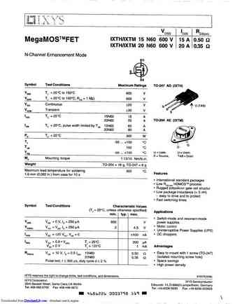
ixfh15n60 ixfh20n60 ixfm15n60 ixfm20n60.pdf
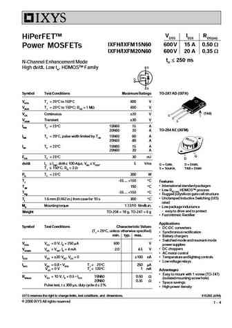
VDSS ID25 RDS(on) HiPerFETTM IXFH/IXFM 15 N60 600 V 15 A 0.50 W Power MOSFETs IXFH/IXFM 20 N60 600 V 20 A 0.35 W trr 250 ns N-Channel Enhancement Mode High dv/dt, Low trr, HDMOSTM Family Symbol Test Conditions Maximum Ratings TO-247 AD (IXFH) VDSS TJ = 25 C to 150 C 600 V VDGR TJ = 25 C to 150 C; RGS = 1 MW 600 V (TAB) VGS Continuous 20 V VGSM Transient 30 V ID25 TC = 2
ixdh35n60bd1.pdf

IXDP 35N60 B VCES = 600 V IGBT IXDH 35N60 B IC25 = 60 A with optional Diode IXDH 35N60 BD1 VCE(sat) typ = 2.1 V High Speed, Low Saturation Voltage C C TO-247 AD IXDH ... G G G E E C C (TAB) E IXDH 35N60 B IXDH 35N60 BD1 IXDP 35N60 B Symbol Conditions Maximum Ratings TO-220 AB IXDP ... VCES TJ = 25 C to 150 C 600 V VCGR TJ = 25 C to 150 C; RGE = 20 kW 600 V G C E VG
ixxh75n60b3d1.pdf
Preliminary Technical Information XPTTM 600V IGBT VCES = 600V IXXH75N60B3D1 GenX3TM w/ Diode IC110 = 75A VCE(sat) 1.85V tfi(typ) = 125ns Extreme Light Punch Through IGBT for 5-30 kHz Switching TO-247 AD Symbol Test Conditions Maximum Ratings VCES TJ = 25 C to 175 C 600 V VCGR TJ = 25 C to 175 C, RGE = 1M 600 V G VGES Continuous 20 V C Tab E
fgh75n60uf.pdf
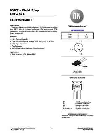
IGBT - Field Stop 600 V, 75 A FGH75N60UF Description Using novel field stop IGBT technology, ON Semiconductor s field stop IGBTs offer the optimum performance for solar inverter, UPS, www.onsemi.com welder and PFC applications where low conduction and switching losses are essential. VCES IC Features 600 V 75 A High Current Capability C Low Saturation Voltage VCE(sat) =
fgb5n60undf.pdf

Is Now Part of To learn more about ON Semiconductor, please visit our website at www.onsemi.com Please note As part of the Fairchild Semiconductor integration, some of the Fairchild orderable part numbers will need to change in order to meet ON Semiconductor s system requirements. Since the ON Semiconductor product management systems do not have the ability to manage part nomenclatur
fcd5n60 fcu5n60.pdf

Is Now Part of To learn more about ON Semiconductor, please visit our website at www.onsemi.com Please note As part of the Fairchild Semiconductor integration, some of the Fairchild orderable part numbers will need to change in order to meet ON Semiconductor s system requirements. Since the ON Semiconductor product management systems do not have the ability to manage part nomenclatur
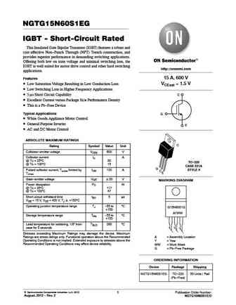
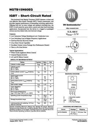
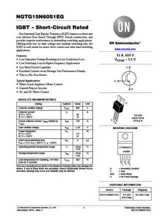
ngtg15n60s1.pdf
NGTG15N60S1EG IGBT - Short-Circuit Rated This Insulated Gate Bipolar Transistor (IGBT) features a robust and cost effective Non-Punch Through (NPT) Trench construction, and provides superior performance in demanding switching applications. Offering both low on state voltage and minimal switching loss, the IGBT is well suited for motor drive control and other hard switching http //onsemi.
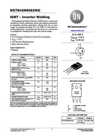
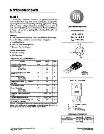
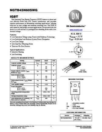
ngtb45n60s1wg.pdf

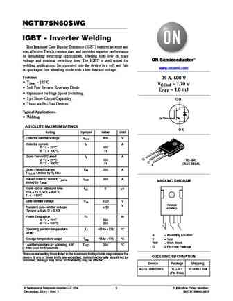
NGTB45N60S1WG IGBT - Inverter Welding This Insulated Gate Bipolar Transistor (IGBT) features a robust and cost effective Trench construction, and provides superior performance in demanding switching applications, offering both low on state voltage and minimal switching loss. The IGBT is well suited for welding applications. Incorporated into the device is a soft and fast www.onsemi.com
ngtb15n60eg.pdf
NGTB15N60EG IGBT - Short-Circuit Rated This Insulated Gate Bipolar Transistor (IGBT) features a robust and cost effective Non-Punch Through (NPT) Trench construction, and provides superior performance in demanding switching applications. Offering both low on state voltage and minimal switching loss, the IGBT is well suited for motor drive control and other hard switching http //onsemi.co
fgpf15n60undf.pdf

Is Now Part of To learn more about ON Semiconductor, please visit our website at www.onsemi.com Please note As part of the Fairchild Semiconductor integration, some of the Fairchild orderable part numbers will need to change in order to meet ON Semiconductor s system requirements. Since the ON Semiconductor product management systems do not have the ability to manage part nomenclatur
ngtb45n60s2wg.pdf
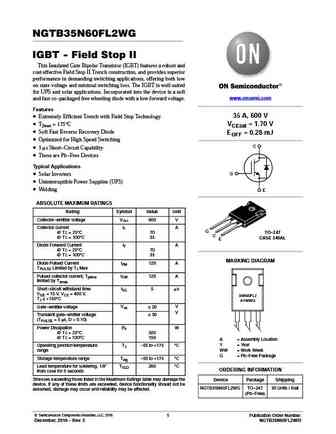
NGTB45N60S2WG IGBT - Inverter Welding This Insulated Gate Bipolar Transistor (IGBT) features a robust and cost effective Trench construction, and provides superior performance in demanding switching applications, offering both low on state voltage and minimal switching loss. The IGBT is well suited for welding applications. Incorporated into the device is a soft and fast www.onsemi.com
fdp5n60nz fdpf5n60nz.pdf

Is Now Part of To learn more about ON Semiconductor, please visit our website at www.onsemi.com Please note As part of the Fairchild Semiconductor integration, some of the Fairchild orderable part numbers will need to change in order to meet ON Semiconductor s system requirements. Since the ON Semiconductor product management systems do not have the ability to manage part nomenclatur
sgh15n60rufd.pdf
IGBT SGH15N60RUFD Short Circuit Rated IGBT General Description Features Fairchild's RUFD series of Insulated Gate Bipolar Short circuit rated 10us @ TC = 100 C, VGE = 15V Transistors (IGBTs) provide low conduction and switching High speed switching losses as well as short circuit ruggedness. The RUFD Low saturation voltage VCE(sat) = 2.2 V @ IC = 15A series is designed f
ngtb75n60fl2wg.pdf
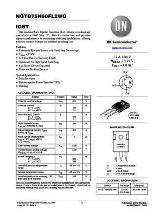
NGTB75N60FL2WG IGBT This Insulated Gate Bipolar Transistor (IGBT) features a robust and cost effective Field Stop (FS) Trench construction, and provides superior performance in demanding switching applications, offering both low on state voltage and minimal switching loss. Features www.onsemi.com Extremely Efficient Trench with Field Stop Technology TJmax = 175 C 75 A, 600 V
ngtb75n60fl2.pdf

NGTB75N60FL2WG IGBT This Insulated Gate Bipolar Transistor (IGBT) features a robust and cost effective Field Stop (FS) Trench construction, and provides superior performance in demanding switching applications, offering both low on state voltage and minimal switching loss. Features www.onsemi.com Extremely Efficient Trench with Field Stop Technology TJmax = 175 C 75 A, 600 V
ngtb45n60s.pdf
NGTB45N60SWG IGBT This Insulated Gate Bipolar Transistor (IGBT) features a robust and cost effective Field Stop (FS) Trench construction, and provides superior performance in demanding switching applications, offering both low on state voltage and minimal switching loss. The IGBT is well suited for half bridge resonant applications. Incorporated into the device is a soft and fast co-pack
ngtb45n60s1.pdf

NGTB45N60S1WG IGBT - Inverter Welding This Insulated Gate Bipolar Transistor (IGBT) features a robust and cost effective Trench construction, and provides superior performance in demanding switching applications, offering both low on state voltage and minimal switching loss. The IGBT is well suited for welding applications. Incorporated into the device is a soft and fast www.onsemi.com
ngtb35n60fl2wg.pdf
NGTB35N60FL2WG IGBT - Field Stop II This Insulated Gate Bipolar Transistor (IGBT) features a robust and cost effective Field Stop II Trench construction, and provides superior performance in demanding switching applications, offering both low on state voltage and minimal switching loss. The IGBT is well suited for UPS and solar applications. Incorporated into the device is a soft www.ons
ngtb15n60s1eg.pdf
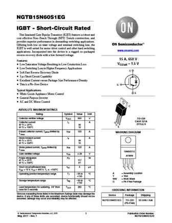
NGTB15N60S1EG IGBT - Short-Circuit Rated This Insulated Gate Bipolar Transistor (IGBT) features a robust and cost effective Non-Punch Through (NPT) Trench construction, and provides superior performance in demanding switching applications. Offering both low on state voltage and minimal switching loss, the IGBT is well suited for motor drive control and other hard switching www.onsemi.com
fgp5n60ls.pdf

Is Now Part of To learn more about ON Semiconductor, please visit our website at www.onsemi.com Please note As part of the Fairchild Semiconductor integration, some of the Fairchild orderable part numbers will need to change in order to meet ON Semiconductor s system requirements. Since the ON Semiconductor product management systems do not have the ability to manage part nomenclatur
fcp165n60e.pdf

Is Now Part of To learn more about ON Semiconductor, please visit our website at www.onsemi.com Please note As part of the Fairchild Semiconductor integration, some of the Fairchild orderable part numbers will need to change in order to meet ON Semiconductor s system requirements. Since the ON Semiconductor product management systems do not have the ability to manage part nomenclatur
fqd5n60c fqu5n60c.pdf
FQD5N60C / FQU5N60C N-Channel QFET MOSFET 600 V, 2.8 A, 2.5 Features Description 2.8 A, 600 V, RDS(on) = 2.5 (Max.) @ VGS = 10 V, ID = 1.4 A This N-Channel enhancement mode power MOSFET is produced using ON Semiconductor s proprietary planar Low Gate Charge ( Typ. 15 nC) stripe and DMOS technology. This advanced MOSFET Low Crss (Typ. 6.5 pF) technology has bee
fgp15n60undf.pdf

Is Now Part of To learn more about ON Semiconductor, please visit our website at www.onsemi.com Please note As part of the Fairchild Semiconductor integration, some of the Fairchild orderable part numbers will need to change in order to meet ON Semiconductor s system requirements. Since the ON Semiconductor product management systems do not have the ability to manage part nomenclatur
ngtb05n60r2dt4g.pdf
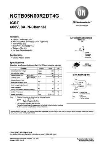
NGTB05N60R2DT4G IGBT www.onsemi.com 600V, 8A, N-Channel Features Electrical Connection Reverse Conducting II IGBT N-Channel IGBT VCE(sat)=1.65V (typ) [IC=5A, VGE=15V] 2,4 IGBT tf=95ns (typ) Diode VF=1.5V (typ) [IF=5A] Diode trr=70ns (typ) 5 s Short Circuit Capability 1 1 Gate 2 Collector Applications 3 Emitter 3 4 Collector Ge
fqp5n60c fqpf5n60c.pdf

TM QFET FQP5N60C/FQPF5N60C 600V N-Channel MOSFET General Description Features These N-Channel enhancement mode power field effect 4.5A, 600V, RDS(on) = 2.5 @VGS = 10 V transistors are produced using Fairchild s proprietary, Low gate charge ( typical 15 nC) planar stripe, DMOS technology. Low Crss ( typical 6.5 pF) This advanced technology has been especially tailored t
ngtb75n60s.pdf

NGTB75N60SWG IGBT - Inverter Welding This Insulated Gate Bipolar Transistor (IGBT) features a robust and cost effective Trench construction, and provides superior performance in demanding switching applications, offering both low on state voltage and minimal switching loss. The IGBT is well suited for welding applications. Incorporated into the device is a soft and fast www.onsemi.com c
ngtb45n60swg.pdf
NGTB45N60SWG IGBT This Insulated Gate Bipolar Transistor (IGBT) features a robust and cost effective Field Stop (FS) Trench construction, and provides superior performance in demanding switching applications, offering both low on state voltage and minimal switching loss. The IGBT is well suited for half bridge resonant applications. Incorporated into the device is a soft and fast co-pack
fqb5n60ctm ws.pdf
June 2015 FQB5N60CTM_WS N-Channel QFET MOSFET 600 V, 4.5 A, 2.5 Features Description 4.5 A, 600 V, RDS(on) = 2.5 (Max.) @VGS = 10 V, ID = 2.1 A This N-Channel enhancement mode power MOSFET is produced using Fairchild Semiconductor s proprietary planar Low Gate Charge (Typ. 15 nC) stripe and DMOS technology. This advanced MOSFET Low Crss (Typ. 6.5 pF) technology
ngtb45n60s2.pdf

NGTB45N60S2WG IGBT - Inverter Welding This Insulated Gate Bipolar Transistor (IGBT) features a robust and cost effective Trench construction, and provides superior performance in demanding switching applications, offering both low on state voltage and minimal switching loss. The IGBT is well suited for welding applications. Incorporated into the device is a soft and fast www.onsemi.com
fcp25n60n.pdf

Is Now Part of To learn more about ON Semiconductor, please visit our website at www.onsemi.com Please note As part of the Fairchild Semiconductor integration, some of the Fairchild orderable part numbers will need to change in order to meet ON Semiconductor s system requirements. Since the ON Semiconductor product management systems do not have the ability to manage part nomenclatur
ngtb15n60s1.pdf
NGTB15N60S1EG IGBT - Short-Circuit Rated This Insulated Gate Bipolar Transistor (IGBT) features a robust and cost effective Non-Punch Through (NPT) Trench construction, and provides superior performance in demanding switching applications. Offering both low on state voltage and minimal switching loss, the IGBT is well suited for motor drive control and other hard switching http //onsemi.
fca35n60.pdf

Is Now Part of To learn more about ON Semiconductor, please visit our website at www.onsemi.com Please note As part of the Fairchild Semiconductor integration, some of the Fairchild orderable part numbers will need to change in order to meet ON Semiconductor s system requirements. Since the ON Semiconductor product management systems do not have the ability to manage part nomenclatur
ngtg15n60s1eg.pdf
NGTG15N60S1EG IGBT - Short-Circuit Rated This Insulated Gate Bipolar Transistor (IGBT) features a robust and cost effective Non-Punch Through (NPT) Trench construction, and provides superior performance in demanding switching applications. Offering both low on state voltage and minimal switching loss, the IGBT is well suited for motor drive control and other hard switching www.onsemi.com
fcp125n60e.pdf

Is Now Part of To learn more about ON Semiconductor, please visit our website at www.onsemi.com Please note As part of the Fairchild Semiconductor integration, some of the Fairchild orderable part numbers will need to change in order to meet ON Semiconductor s system requirements. Since the ON Semiconductor product management systems do not have the ability to manage part nomenclatur
ngtb75n60swg.pdf
NGTB75N60SWG IGBT - Inverter Welding This Insulated Gate Bipolar Transistor (IGBT) features a robust and cost effective Trench construction, and provides superior performance in demanding switching applications, offering both low on state voltage and minimal switching loss. The IGBT is well suited for welding applications. Incorporated into the device is a soft and fast www.onsemi.com c
fdu5n60nztu.pdf
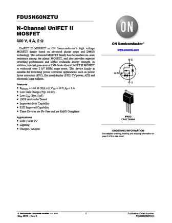
FDU5N60NZTU N-Channel UniFET II MOSFET 600 V, 4 A, 2 W UniFET II MOSFET is ON Semiconductor s high voltage www.onsemi.com MOSFET family based on advanced planar stripe and DMOS technology. This advanced MOSFET family has the smallest on-state resistance among the planar MOSFET, and also provides superior D switching performance and higher avalanche energy strength. In addition, int
5n60l-tf3t-t 5n60g-tf3t-t 5n60l-tm3-t 5n60g-tm3-t 5n60l-tn3-r 5n60g-tn3-r 5n60l-k08-5060-r 5n60g-k08-5060-r.pdf

UNISONIC TECHNOLOGIES CO., LTD 5N60 Power MOSFET 5A, 600V N-CHANNEL POWER MOSFET DESCRIPTION The UTC 5N60 is a high voltage power MOSFET and is designed to have better characteristics, such as fast switching time, low gate charge, low on-state resistance and have a high rugged avalanche characteristics. This power MOSFET is usually used at high speed switching applications
5n60l-ta3-t 5n60g-ta3-t 5n60l-tf1-t 5n60g-tf1-t 5n60l-tf2-t 5n60g-tf2-t 5n60l-tf3-t 5n60g-tf3-t.pdf

UNISONIC TECHNOLOGIES CO., LTD 5N60 Power MOSFET 5A, 600V N-CHANNEL POWER MOSFET DESCRIPTION The UTC 5N60 is a high voltage power MOSFET and is designed to have better characteristics, such as fast switching time, low gate charge, low on-state resistance and have a high rugged avalanche characteristics. This power MOSFET is usually used at high speed switching applications
15n60.pdf
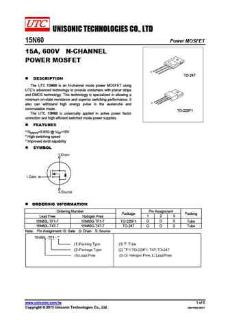
UNISONIC TECHNOLOGIES CO., LTD 15N60 Power MOSFET 15A, 600V N-CHANNEL POWER MOSFET 1 TO-247 DESCRIPTION The UTC 15N60 is an N-channel mode power MOSFET using UTC s advanced technology to provide costumers with planar stripe and DMOS technology. This technology is specialized in allowing a minimum on-state resistance and superior switching performance. It 1 also can with
fgw35n60h.pdf
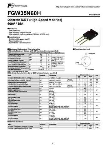
http //www.fujielectric.com/products/semiconductor/ FGW35N60H Discrete IGBT Discrete IGBT (High-Speed V series) 600V / 35A Features Low power loss Low switching surge and noise High reliability, high ruggedness (RBSOA, SCSOA etc.) Applications Uninterruptible power supply Power coditionner Power factor correction circuit Maximum Ratings and Characteristics Equivalent circuit Absol
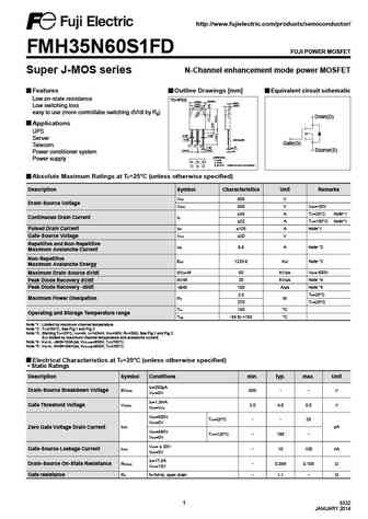
fmh35n60s1fd.pdf
http //www.fujielectric.com/products/semiconductor/ FMH35N60S1FD FUJI POWER MOSFET Super J-MOS series N-Channel enhancement mode power MOSFET Features Outline Drawings [mm] Equivalent circuit schematic Low on-state resistance TO-3P(Q) 3.2 0.1 15.5max 1.5 0.2 13 0.2 4.5 0.2 Low switching loss 10 0.2 easy to use (more controllabe switching dV/dt by R ) g Drain(D) Applica
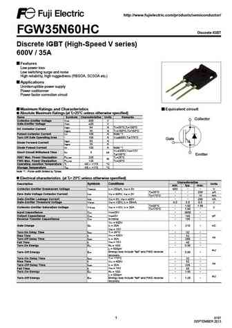
fgw35n60hc.pdf
http //www.fujielectric.com/products/semiconductor/ FGW35N60HC Discrete IGBT Discrete IGBT (High-Speed V series) 600V / 35A Features Low power loss Low switching surge and noise High reliability, high ruggedness (RBSOA, SCSOA etc.) Applications Uninterruptible power supply Power coditionner Power factor correction circuit Maximum Ratings and Characteristics Equivalent circuit Abso
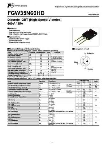
fgw35n60hd.pdf
http //www.fujielectric.com/products/semiconductor/ FGW35N60HD Discrete IGBT Discrete IGBT (High-Speed V series) 600V / 35A Features Low power loss Low switching surge and noise High reliability, high ruggedness (RBSOA, SCSOA etc.) Applications Uninterruptible power supply Power coditionner Power factor correction circuit Maximum Ratings and Characteristics Equivalent circuit Abso
fmp05n60e.pdf

FMP05N60E FUJI POWER MOSFET Super FAP-E3 series N-CHANNEL SILICON POWER MOSFET Features Outline Drawings [mm] Equivalent circuit schematic Maintains both low power loss and low noise TO-220AB Lower R (on) characteristic DS More controllable switching dv/dt by gate resistance Drain(D) Smaller V ringing waveform during switching GS Narrow band of the gate threshold voltage (3.0 0.5V)
fmc05n60e.pdf
FMC05N60E FUJI POWER MOSFET Super FAP-E3 series N-CHANNEL SILICON POWER MOSFET Features Outline Drawings [mm] Equivalent circuit schematic Maintains both low power loss and low noise T-Pack(S) Lower R (on) characteristic DS More controllable switching dv/dt by gate resistance Drain(D) Smaller V ringing waveform during switching GS Narrow band of the gate threshold voltage (3.0 0.5V)
fgw75n60hd.pdf
http //www.fujielectric.com/products/semiconductor/ FGW75N60HD Discrete IGBT Discrete IGBT (High-Speed V series) 600V / 75A Features Low power loss Low switching surge and noise High reliability, high ruggedness (RBSOA, SCSOA etc.) Applications Uninterruptible power supply Power coditionner Power factor correction circuit Maximum Ratings and Characteristics Equivalent circuit Abso
fmv05n60e.pdf
FMV05N60E FUJI POWER MOSFET Super FAP-E3 series N-CHANNEL SILICON POWER MOSFET Features Outline Drawings [mm] Equivalent circuit schematic Maintains both low power loss and low noise TO-220F(SLS) Lower R (on) characteristic DS More controllable switching dv/dt by gate resistance Drain(D) Smaller V ringing waveform during switching GS Narrow band of the gate threshold voltage (3.0 0.
fgw75n60h.pdf

http //www.fujielectric.com/products/semiconductor/ FGW75N60H Discrete IGBT Discrete IGBT (High-Speed V series) 600V / 75A Features Low power loss Low switching surge and noise High reliability, high ruggedness (RBSOA, SCSOA etc.) Applications Uninterruptible power supply Power coditionner Power factor correction circuit Maximum Ratings and Characteristics Equivalent circuit Absol
fmi05n60e.pdf
FMI05N60E FUJI POWER MOSFET Super FAP-E3 series N-CHANNEL SILICON POWER MOSFET Features Outline Drawings [mm] Equivalent circuit schematic Maintains both low power loss and low noise T-Pack(L) Lower R (on) characteristic DS More controllable switching dv/dt by gate resistance Drain(D) Smaller V ringing waveform during switching GS Narrow band of the gate threshold voltage (3.0 0.5V)
fgw85n60rb.pdf
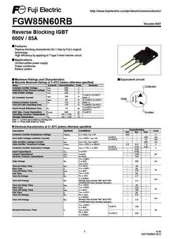
http //www.fujielectric.com/products/semiconductor/ FGW85N60RB Discrete IGBT Reverse Blocking IGBT 600V / 85A Features Reverse blocking characteristic for 1 chip by Fuji's original technology. High efficiency by applying to T-type 3 level inverter circuit. Applications Uninterruptible power supply Power conditioner Battery system Maximum Ratings and Characteristics Equivalent circu
cju05n60b.pdf

JIANGSU CHANGJIANG ELECTRONICS TECHNOLOGY CO., LTD TO-252-2L Plastic-Encapsulate MOSFETS CJU05N60B N-Channel Power MOSFET TO-252-2L GENERAL DESCRIPTION This advanced high voltage MOSFET is designed to stand high energy in the avalanche mode and switch efficiently. This new high energy device also offers a drain-to-source diode fast recovery time. Desighed for high voltage, hi
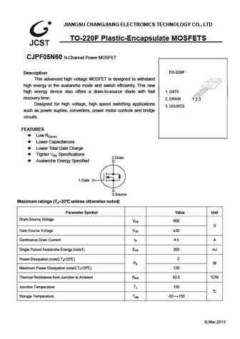
cjpf05n60b.pdf
JIANGSU CHANGJIANG ELECTRONICS TECHNOLOGY CO., LTD TO-220F Plastic-Encapsulate MOSFETS CJPF05N60B N-Channel Power MOSFET TO-220F GENERAL DESCRIPTION This advanced high voltage MOSFET is designed to stand high energy in the avalanche mode and switch efficiently. This new high energy device also offers a drain-to-source diode fast recovery time. Desighed for high voltage, high
cjp05n60.pdf
JIANGSU CHANGJIANG ELECTRONICS TECHNOLOGY CO., LTD TO-220-3L Plastic-Encapsulate MOSFETS CJP05N60 N-Channel Power MOSFET TO-220-3L Description This advanced high voltage MOSFET is designed to withstand high energy in the avalanche mode and switch efficiently. This new high energy device also offers a drain-to-source diode with fast recovery time. Designed for high voltage, h
cjp05n60b.pdf
JIANGSU CHANGJIANG ELECTRONICS TECHNOLOGY CO., LTD TO-220-3L Plastic-Encapsulate MOSFETS CJP05N60B N-Channel Power MOSFET TO-220-3L GENERAL DESCRIPTION This advanced high voltage MOSFET is designed to stand high energy in the avalanche mode and switch efficiently. This new 1. GATE high energy device also offers a drain-to-source diode fast 2. DRAIN recovery time. Desighed
cjd05n60b.pdf
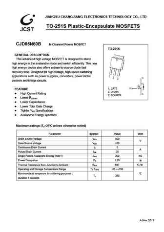
JIANGSU CHANGJIANG ELECTRONICS TECHNOLOGY CO., LTD TO-251S Plastic-Encapsulate MOSFETS CJD05N60B N-Channel Power MOSFET TO-251S GENERAL DESCRIPTION This advanced high voltage MOSFET is designed to stand high energy in the avalanche mode and switch efficiently. This new high energy device also offers a drain-to-source diode fast recovery time. Desighed for high voltage, high s
cju05n60.pdf
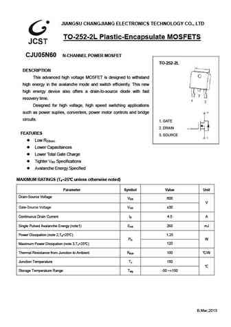
JIANGSU CHANGJIANG ELECTRONICS TECHNOLOGY CO., LTD TO-252-2L Plastic-Encapsulate MOSFETS CJU05N60 N-CHANNEL POWER MOSFET TO-252-2L DESCRIPTION This advanced high voltage MOSFET is designed to withstand high energy in the avalanche mode and switch efficiently. This new high energy device also offers a drain-to-source diode with fast recovery time. Designed for high voltage,
cjpf05n60.pdf
JIANGSU CHANGJIANG ELECTRONICS TECHNOLOGY CO., LTD TO-220F Plastic-Encapsulate MOSFETS CJPF05N60 N-Channel Power MOSFET TO-220F Description This advanced high voltage MOSFET is designed to withstand high energy in the avalanche mode and switch efficiently. This new high energy device also offers a drain-to-source diode with fast 1. GATE recovery time. 2. DRAIN 123 Des
kgf15n60fda.pdf
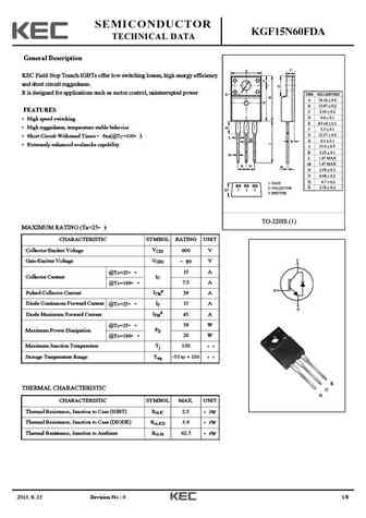
SEMICONDUCTOR KGF15N60FDA TECHNICAL DATA General Description KEC Field Stop Trench IGBTs offer low switching losses, high energy efficiency and short circuit ruggedness. It is designed for applications such as motor control, uninterrupted power FEATURES High speed switching High ruggedness, temperature stable behavior Short Circuit Withstand Times 5us(@TC=100 ) Extremel
kf5n60p kf5n60f.pdf
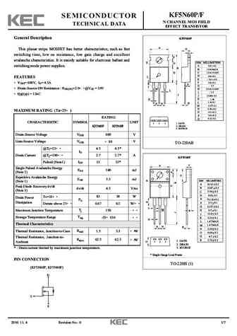
KF5N60P/F SEMICONDUCTOR N CHANNEL MOS FIELD TECHNICAL DATA EFFECT TRANSISTOR General Description KF5N60P A This planar stripe MOSFET has better characteristics, such as fast O C switching time, low on resistance, low gate charge and excellent F avalanche characteristics. It is mainly suitable for electronic ballast and E DIM MILLIMETERS G _ switching mode power supplies. A 9.9
kgf75n60kdb.pdf
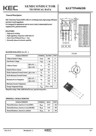
SEMICONDUCTOR KGF75N60KDB TECHNICAL DATA General Description KEC Field Stop Trench IGBTs offer low switching losses, high energy efficiency and short circuit ruggedness. It is designed for applications such as motor control, uninterrupted power supplies(UPS), general inverters. FEATURES High speed switching High ruggedness, temperature stable behavior Short Circuit Withstand T
kf5n60p-f.pdf

KF5N60P/F SEMICONDUCTOR N CHANNEL MOS FIELD TECHNICAL DATA EFFECT TRANSISTOR General Description KF5N60P A This planar stripe MOSFET has better characteristics, such as fast O C switching time, low on resistance, low gate charge and excellent F avalanche characteristics. It is mainly suitable for electronic ballast and E DIM MILLIMETERS G _ switching mode power supplies. A 9.9
kf5n60fz.pdf
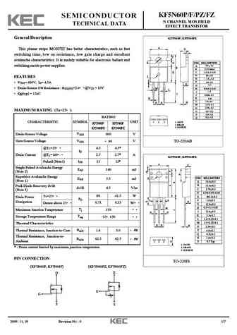
KF5N60P/F/PZ/FZ SEMICONDUCTOR N CHANNEL MOS FIELD TECHNICAL DATA EFFECT TRANSISTOR General Description KF5N60P, KF5N60PZ A This planar stripe MOSFET has better characteristics, such as fast O C switching time, low on resistance, low gate charge and excellent F avalanche characteristics. It is mainly suitable for electronic ballast and E DIM MILLIMETERS G _ + switching mode pow
khb7d5n60p1 f1 f2.pdf
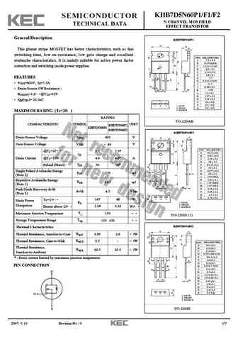
KHB7D5N60P1/F1/F2 SEMICONDUCTOR N CHANNEL MOS FIELD TECHNICAL DATA EFFECT TRANSISTOR General Description KHB7D0N60P1 This planar stripe MOSFET has better characteristics, such as fast switching time, low on resistance, low gate charge and excellent avalanche characteristics. It is mainly suitable for active power factor correction and switching mode power supplies. FEATURES VDSS
kf5n60d i.pdf
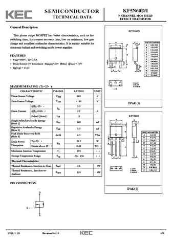
KF5N60D/I SEMICONDUCTOR N CHANNEL MOS FIELD TECHNICAL DATA EFFECT TRANSISTOR General Description KF5N60D This planar stripe MOSFET has better characteristics, such as fast switching time, fast reverse recovery time, low on resistance, low gate A K DIM MILLIMETERS charge and excellent avalanche characteristics. It is mainly suitable for L C D _ A 6.60 + 0.20 _ B 6.10 + 0.20 ele
khb4d5n60p f f2.pdf
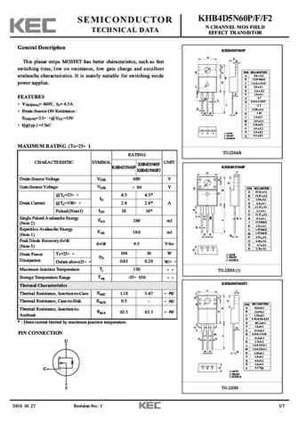
KHB4D5N60P/F/F2 SEMICONDUCTOR N CHANNEL MOS FIELD TECHNICAL DATA EFFECT TRANSISTOR General Description KHB4D5N60P A O This planar stripe MOSFET has better characteristics, such as fast C F switching time, low on resistance, low gate charge and excellent E DIM MILLIMETERS G _ A 9.9 + 0.2 avalanche characteristics. It is mainly suitable for switching mode B B 15.95 MAX Q pow
kgt15n60fda.pdf
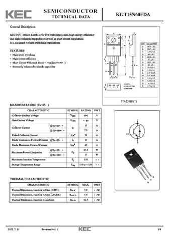
SEMICONDUCTOR KGT15N60FDA TECHNICAL DATA General Description KEC NPT Trench IGBTs offer low switching losses, high energy efficiency and high avalanche ruggedness as well as short circuit ruggedness. It is designed for hard switching applications. FEATURES High speed switching High system efficiency Short Circuit Withstand Times 5us(@TC=100 ) Extremely enhanced avalanch
h05n60.pdf
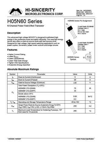
Spec. No. MOS200603 HI-SINCERITY Issued Date 2006.02.01 Revised Date 2006.02.07 MICROELECTRONICS CORP. Page No. 1/5 H05N60 Series Pin Assignment H05N60 Series Tab N-Channel Power Field Effect Transistor 3-Lead Plastic TO-220AB Package Code E Pin 1 Gate Pin 2 & Tab Drain Description Pin 3 Source 3 This advanced high voltage MOSFET is designed to withstand high 2 1
aot5n60.pdf
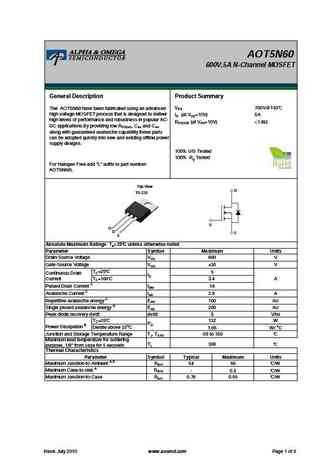
AOT5N60 600V,5A N-Channel MOSFET General Description Product Summary VDS 700V@150 The AOT5N60 have been fabricated using an advanced high voltage MOSFET process that is designed to deliver ID (at VGS=10V) 5A high levels of performance and robustness in popular AC- RDS(ON) (at VGS=10V)
sss5n60.pdf
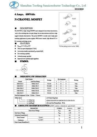
Shenzhen Tuofeng Semiconductor Technology Co., Ltd N60 SSS5N60 4 Amps 600Volts 4 Amps 600Volts 4 Amps 600Volts 4 Amps 600Volts N-CHANNEL MOSFET N-CHANNEL MOSFET N-CHANNEL MOSFET N-CHANNEL MOSFET DESCRIPTION The SSS5N60 is a high voltage MOSFET and is designed to have better characteristics, such as fast switching time, low gate charge, low on-state resistance and have a high
sif5n60c 1.pdf
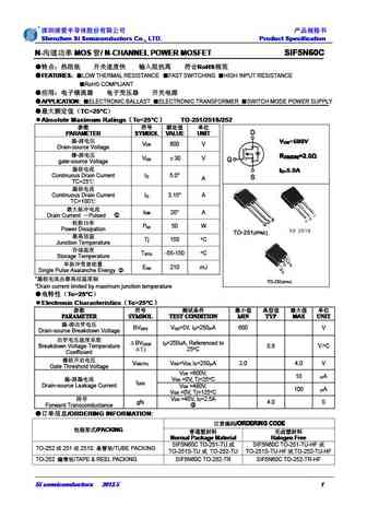
Shenzhen SI Semiconductors Co., LTD. Product Specification Shenzhen SI Semiconductors Co., LTD. Product Specification Shenzhen SI Semiconductors Co., LTD. Product Specification Shenzhen SI Semiconductors Co., LTD. Product Specification N- MOS / N-CHANNEL POWER MOSFET SIF5N60C N- MOS / N-CHANNEL POWER MOSFET SIF5N60C N- MOS / N-CHANN
sif5n60c.pdf
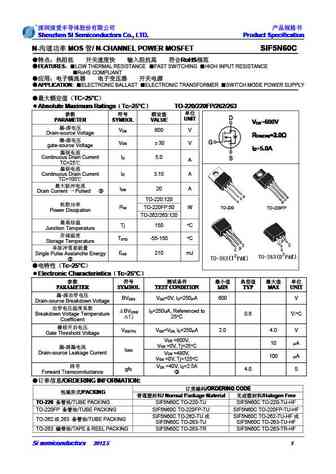
Shenzhen SI Semiconductors Co., LTD. Product Specification Shenzhen SI Semiconductors Co., LTD. Product Specification Shenzhen SI Semiconductors Co., LTD. Product Specification Shenzhen SI Semiconductors Co., LTD. Product Specification N- MOS / N-CHANNEL POWER MOSFET SIF5N60C N- MOS / N-CHANNEL POWER MOSFET SIF5N60C N
jcs15n60ch jcs15n60fh jcs15n60bh jcs15n60sh.pdf
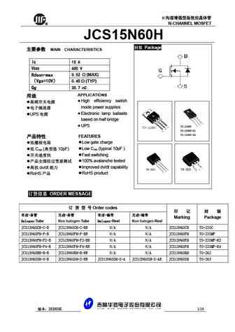
N R N-CHANNEL MOSFET JCS15N60H Package MAIN CHARACTERISTICS ID 15 A VDSS 600 V 0.52 (MAX) Rdson-max Vgs=10V 0.45 (TYP) Qg 35.7 nC APPLICATIONS High efficiency switch mode power supplies Electronic lamp ballasts UPS based o
jcs5n60v jcs5n60r jcs5n60c jcs5n60f.pdf
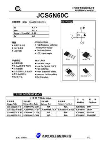
N R N-CHANNEL MOSFET JCS5N60C Package MAIN CHARACTERISTICS ID 4.0 A VDSS 600 V Rdson Vgs=10V 2.5 Qg 9nC APPLICATIONS High frequency switching mode power supply Electronic ballast LED LED power supply FEATURES
mp15n60eif mp15n60eib mp15n60eis mp15n60eic.pdf
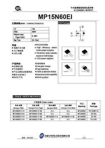
N R N-CHANNEL MOSFET MP15N60EI Package MAIN CHARACTERISTICS ID 15A VDSS 600V Rdson-max 0.48 Vgs=10V Qg-Typ 53.73nC APPLICATIONS High efficiency switch mode power supplies Electronic lamp ballasts LED based on half bridge
jcs5n60vb jcs5n60rb jcs5n60cb jcs5n60fb.pdf
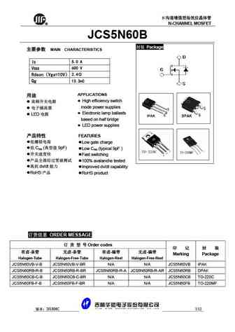
N R N-CHANNEL MOSFET JCS5N60B Package MAIN CHARACTERISTICS ID 5.0 A VDSS 600 V 2.4 Rdson Vgs=10V Qg 13.3nC APPLICATIONS High efficiency switch mode power supplies Electronic lamp ballasts LED based on half bridge LED power su
mtn5n60fp.pdf
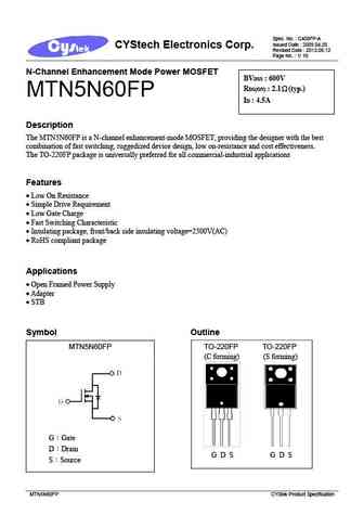
Spec. No. C408FP-A Issued Date 2009.04.20 CYStech Electronics Corp. Revised Date 2013.08.12 Page No. 1/ 10 N-Channel Enhancement Mode Power MOSFET BVDSS 600V RDS(ON) 2.1 (typ.) MTN5N60FP ID 4.5A Description The MTN5N60FP is a N-channel enhancement-mode MOSFET, providing the designer with the best combination of fast switching, ruggedized device design, low
mtn5n60i3.pdf
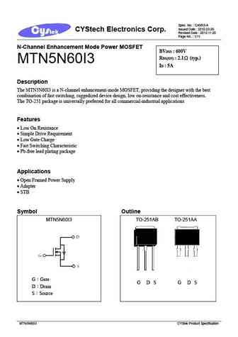
Spec. No. C408I3-A Issued Date 2010.03.09 CYStech Electronics Corp. Revised Date 2012.11.20 Page No. 1/11 N-Channel Enhancement Mode Power MOSFET BVDSS 600V RDS(ON) 2.1 (typ.) MTN5N60I3 ID 5A Description The MTN5N60I3 is a N-channel enhancement-mode MOSFET, providing the designer with the best combination of fast switching, ruggedized device design, low on
mtn5n60e3.pdf
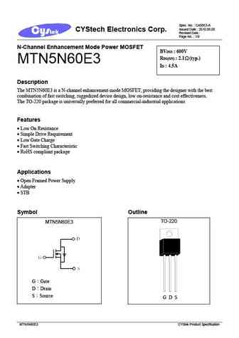
Spec. No. C408E3-A Issued Date 2010.09.08 CYStech Electronics Corp. Revised Date Page No. 1/9 N-Channel Enhancement Mode Power MOSFET BVDSS 600V RDS(ON) 2.1 (typ.) MTN5N60E3 ID 4.5A Description The MTN5N60E3 is a N-channel enhancement-mode MOSFET, providing the designer with the best combination of fast switching, ruggedized device design, low on-resistance
mtn5n60j3.pdf
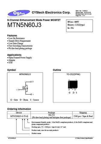
Spec. No. C408J3 Issued Date 2010.03.09 CYStech Electronics Corp. Revised Date 2013.12.26 Page No. 1/11 N-Channel Enhancement Mode Power MOSFET BVDSS 600V RDS(ON) 2.1 (typ.) MTN5N60J3 ID 5A Features Low On Resistance Simple Drive Requirement Low Gate Charge Fast Switching Characteristic Pb-free lead plating package Applications
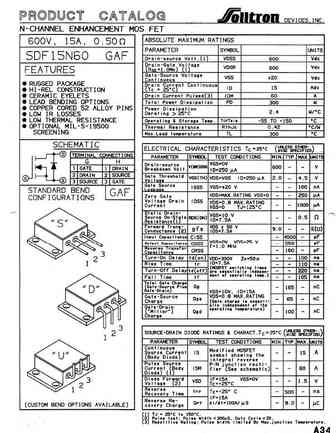
ssf5n60d.pdf
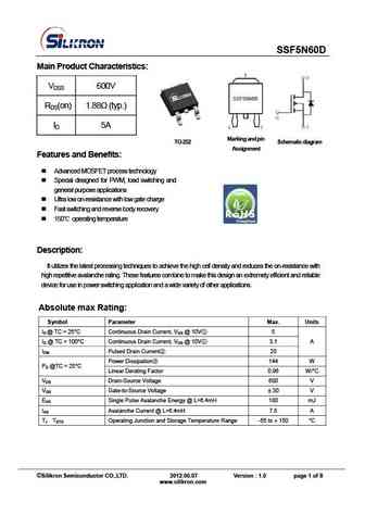
SSF5N60D Main Product Characteristics VDSS 600V RDS(on) 1.88 (typ.) ID 5A TO-252 Marking a nd p in Sche ma ti c di agr a m Assignment Features and Benefits Advanced MOSFET process technology Special designed for PWM, load switching and general purpose applications Ultra low on-resistance with low gate charge Fast switching and reverse body recovery
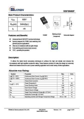
ssf5n60g.pdf
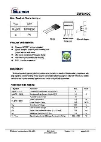
SSF5N60G Main Product Characteristics VDSS 600V RDS(on) 1.88 (typ.) ID 5A TO-251 Marking a nd p in Sche ma ti c di agr a m Assignment Features and Benefits Advanced MOSFET process technology Special designed for PWM, load switching and general purpose applications Ultra low on-resistance with low gate charge Fast switching and reverse body recovery
brf5n60.pdf
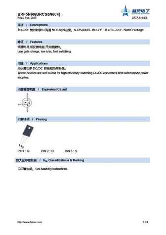
BRF5N60(BRCS5N60F) Rev.C Feb.-2015 DATA SHEET / Descriptions TO-220F N MOS N-CHANNEL MOSFET in a TO-220F Plastic Package. / Features , , Low gate charge, low crss, fast switching. / Applications DC/DC These devices are well suited for hi
brcs25n60ph.pdf
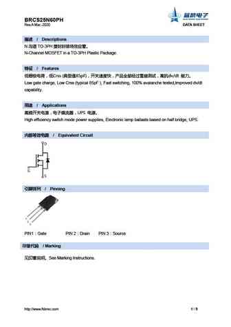
BRCS25N60PH Rev.A Mar.-2020 DATA SHEET / Descriptions N TO-3PH N-Channel MOSFET in a TO-3PH Plastic Package. / Features Crss ( 85pF) dv/dt Low gate charge, Low Crss (typical 85pF ), Fast switching, 100% avalanche tested,Improved dv/dt
brd5n60.pdf
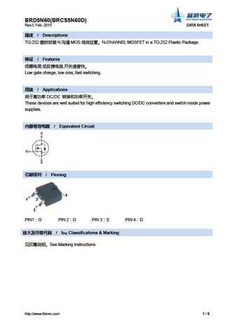
BRD5N60(BRCS5N60D) Rev.C Feb.-2015 DATA SHEET / Descriptions TO-252 N MOS N-CHANNEL MOSFET in a TO-252 Plastic Package. / Features , , Low gate charge, low crss, fast switching. / Applications DC/DC These devices are well suited for high
bri5n60.pdf
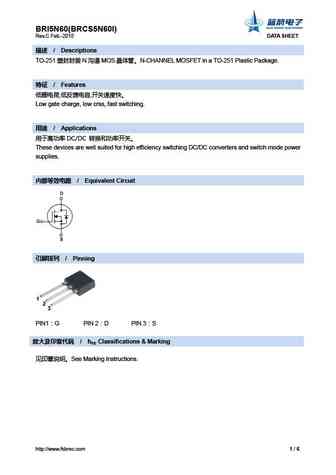
BRI5N60(BRCS5N60I) Rev.C Feb.-2015 DATA SHEET / Descriptions TO-251 N MOS N-CHANNEL MOSFET in a TO-251 Plastic Package. / Features , , Low gate charge, low crss, fast switching. / Applications DC/DC These devices are well suited for high ef
5n60a 5n60af 5n60g.pdf
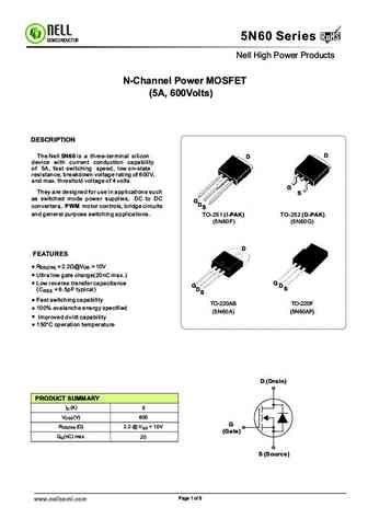
RoHS 5N60 Series RoHS SEMICONDUCTOR Nell High Power Products N-Channel Power MOSFET (5A, 600Volts) DESCRIPTION D The Nell 5N60 is a three-terminal silicon D device with current conduction capability of 5A, fast switching speed, low on-state resistance, breakdown voltage rating of 600V, and max. threshold voltage of 4 volts. G They are designed for use in applications such
hff5n60.pdf
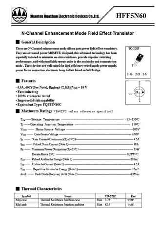
Shantou Huashan Electronic Devices Co.,Ltd. HFF5N60 N-Channel Enhancement Mode Field Effect Transistor General Description These are N-Channel enhancement mode silicon gate power field effect transistors. TO-220F They are advanced power MOSFETs designed, this advanced technology has been especially tailored to minimize on-state resistance, provide superior switching performanc
bt15n60a9f.pdf
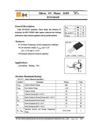
Silicon FS Planar IGBT R BT15N60A9F General Description VCES 600 V Using HUAJING's proprietary Planar design and advanced FS IC 15 A technology, the 600V FSIGBT offers superior conduction and switching Ptot TC=25 25 W performances, high avalanche ruggedness and easy parallel operation. VCE(SAT) 2.1 V Features FS Planar Technology, Positive temperature coeff
cs15n60.pdf
CS15N60 N PD TC=25 280 W 2.3 W/ ID VGS=10V,TC=25 15 A ID VGS=10V,TC=100 9.7 A IDM 60 A VGS 30 V Tjm +150 Tstg -55 +150 RthJC 0.44 /W BVDSS VGS=0V,ID=0.25mA 600 V RDS on VGS=10V,ID=9A 0.46
1d5n60.pdf
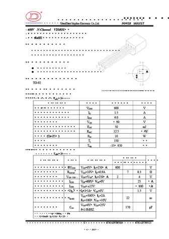
R 1D5N60 www.jdsemi.cn ShenZhen Jingdao Electronic Co.,Ltd. POWER MOSFET 600V N-Channel VDMOS RoHS 1 2 3
kqb5n60.pdf
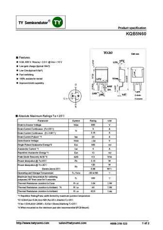
SMD Type IC SMD Type IC SMD Type IC SMD Type IC SMD Type Transistors SMD Type Transistors SMD Type Transistors SMD Type Transistors SMDType SMDType IC Product specification KQB5N60 TO-263 Unit mm Features 4.57+0.2 -0.2 +0.1 5.0A, 600 V. RDS(ON) =2.0 @VGS =10V 1.27-0.1 Low gate charge (typical 16nC) Low Crss(typical 9.0pF) Fast switching +0.1 0.1max 100% avalanche teste
fir5n60fg.pdf
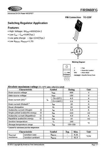
FIR5N60FG Advanced N-Ch Power MOSFET PIN Connection TO-220F Switchng Regulator Application Features High Voltage BVDSS=600V(Min.) Low Crss Crss=9.8F(Typ.) Low gate charge Qg=12nC(Typ.) G D S Low RDS(on) RDS(on)=1.7 D G S Marking Diagram Y = Year A = Assembly Location YAWW WW = Work Week FIR5N60F FIR5N60F = Specific Device Code Absolute maxi
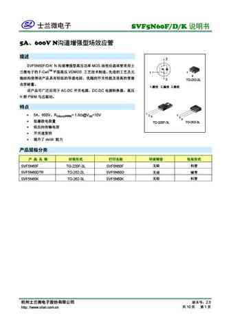
svf5n60t svf5n60f svf5n60d svf5n60mj.pdf
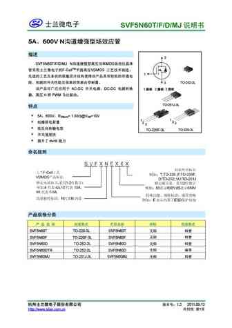
SVF5N60T/F/D/MJ 5A 600V N 2 SVF5N60T/F/D/MJ N MOS F-CellTM VDMOS 1 TO-252-2L 3
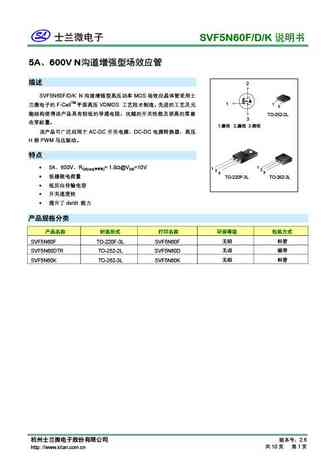
mdf15n60gth mdp15n60gth.pdf
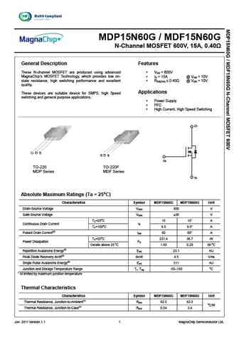
MDP15N60G / MDF15N60G N-Channel MOSFET 600V, 15A, 0.40 General Description Features These N-channel MOSFET are produced using advanced V = 600V DS MagnaChip s MOSFET Technology, which provides low on- I = 15A @ V = 10V D GS state resistance, high switching performance and excellent R 0.40 @ V = 10V DS(ON) GS quality. Applications These devices are sui
msf15n60.pdf
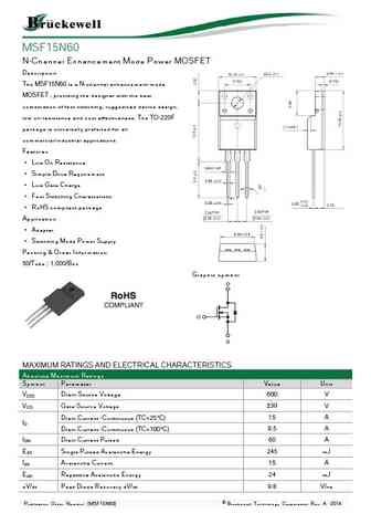
MSF15N60 N-Channel Enhancement Mode Power MOSFET Description The MSF15N60 is a N-channel enhancement-mode MOSFET , providing the designer with the best combination of fast switching, ruggedized device design, low on-resistance and cost effectiveness. The TO-220F package is universally preferred for all commercial-industrial applications Features Low On Resistance S
dms05n60.pdf
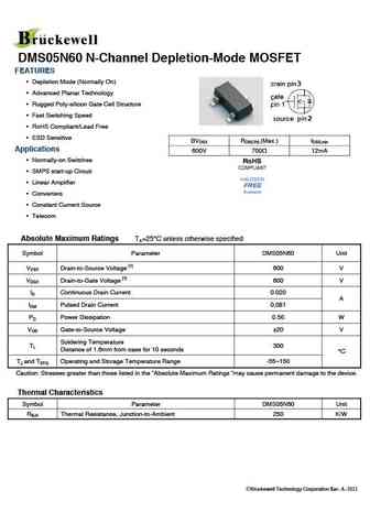
DMS05N60 N-Channel Depletion-Mode MOSFET FEATURES Depletion Mode (Normally On) Advanced Planar Technology Rugged Poly-silicon Gate Cell Structure Fast Switching Speed RoHS Compliant/Lead Free ESD Sensitive BVDSX RDS(ON) (Max.) IDSS,min Applications 600V 700 12mA Normally-on Switches SMPS start-up Circuit Linear Amplifier Con
msf5n60.pdf
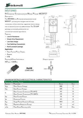
MSF5N60 N-Channel Enhancement Mode Power MOSFET Description The MSF5N60 is a N-channel enhancement-mode MOSFET , providing the designer with the best combination of fast switching, ruggedized device design, low on-resistance and cost effectiveness. The TO-220F package is universally preferred for all commercial-industrial applications Features Low On Resistance Sim
ms5n60.pdf
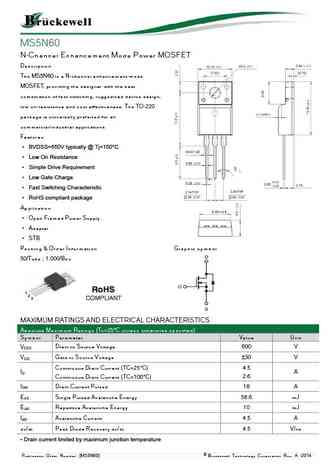
MS5N60 N-Channel Enhancement Mode Power MOSFET Description The MS5N60 is a N-channel enhancement-mode MOSFET, providing the designer with the best combination of fast switching, ruggedized device design, low on-resistance and cost effectiveness. The TO-220 package is universally preferred for all commercial-industrial applications Features BVDSS=650V typically @ Tj=150
ms15n60.pdf
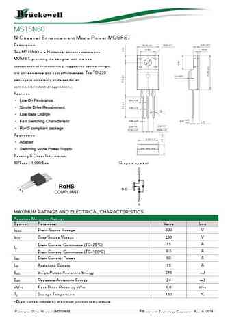
MS15N60 N-Channel Enhancement Mode Power MOSFET Description The MS15N60 is a N-channel enhancement-mode MOSFET, providing the designer with the best combination of fast switching, ruggedized device design, low on-resistance and cost effectiveness. The TO-220 package is universally preferred for all commercial-industrial applications Features Low On Resistance Simpl
msb15n60.pdf
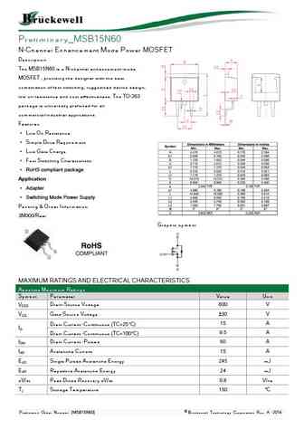
Preliminary_MSB15N60 N-Channel Enhancement Mode Power MOSFET Description The MSB15N60 is a N-channel enhancement-mode MOSFET , providing the designer with the best combination of fast switching, ruggedized device design, low on-resistance and cost effectiveness. The TO-263 package is universally preferred for all commercial-industrial applications Features Low On Resista
wfu5n60.pdf

WFU5N60 WFU5N60 WFU5N60 WFU5N60 Silicon N-Channel MOSFET Silicon N-Channel MOSFET Silicon N-Channel MOSFET Silicon N-Channel MOSFET Features 4.5A,600V,R (Max2.5 )@V =10V DS(on) GS Ultra-low Gate charge(Typical 16nC) Fast Switching Capability 100%Avalanche Tested Maximum Junction Temperature Range(150 ) General Description This Power MOSFET is produced usi
wfu5n60b.pdf
WFU5N60B WFU5N60B WFU5N60B WFU5N60B Silicon N-Channel MOSFET Silicon N-Channel MOSFET Silicon N-Channel MOSFET Silicon N-Channel MOSFET Features 4.5A,600V,R (Max2.4 )@V =10V DS(on) GS Ultra-low Gate charge(Typical 15nC) Fast Switching Capability 100%Avalanche Tested Maximum Junction Temperature Range(150 ) General Description This Power MOSFET is produced
wfd5n60b.pdf
WFD5N60B WFD5N60B WFD5N60B WFD5N60B Silicon N-Channel MOSFET Silicon N-Channel MOSFET Silicon N-Channel MOSFET Silicon N-Channel MOSFET Features 4.5A,600V,R (Max2.4 )@V =10V DS(on) GS Ultra-low Gate charge(Typical 15nC) Fast Switching Capability 100%Avalanche Tested Maximum Junction Temperature Range(150 ) General Description This Power MOSFET is produced
wff15n60.pdf
WFF15N60 WFF15N60 WFF15N60 WFF15N60 Silicon N-Channel MOSFET Silicon N-Channel MOSFET Silicon N-Channel MOSFET Silicon N-Channel MOSFET Features 15A,600V, R (Max0.52 )@V =10V DS(on) GS Ultra-low Gate charge(Typical 36nC) Fast Switching Capability 100%Avalanche Tested Maximum Junction Temperature Range(150 ) General Description This Power MOSFET is produce
wfp5n60b.pdf
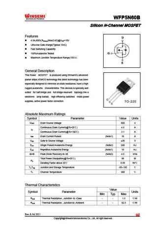
WFP5N60B WFP5N60B WFP5N60B WFP5N60B Silicon N-Channel MOSFET Silicon N-Channel MOSFET Silicon N-Channel MOSFET Silicon N-Channel MOSFET Features 4.5A,600V,R (Max2.4 )@V =10V DS(on) GS Ultra-low Gate charge(Typical 15nC) Fast Switching Capability 100%Avalanche Tested Maximum Junction Temperature Range(150 ) General Description This Power MOSFET is produced
wfd5n60c.pdf
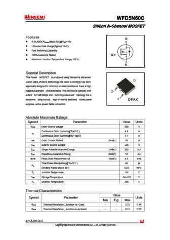
WFD5N60C WFD5N60C WFD5N60C WFD5N60C Silicon N-Channel MOSFET Silicon N-Channel MOSFET Silicon N-Channel MOSFET Silicon N-Channel MOSFET Features 4.5A,600V,R (Max2.5 )@V =10V DS(on) GS Ultra-low Gate charge(Typical 15nC) Fast Switching Capability 100%Avalanche Tested Maximum Junction Temperature Range(150 ) General Description This Power MOSFET is produced
wff5n60c.pdf
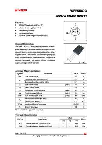
WFF5N60C WFF5N60C WFF5N60C WFF5N60C Silicon N-Channel MOSFET Silicon N-Channel MOSFET Silicon N-Channel MOSFET Silicon N-Channel MOSFET Features 4.5A,600V,R (Max2.5 )@V =10V DS(on) GS Ultra-low Gate charge(Typical 15nC) Fast Switching Capability 100%Avalanche Tested Maximum Junction Temperature Range(150 ) General Description This Power MOSFET is produced
wff5n60b.pdf
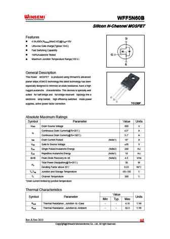
WFF5N60B WFF5N60B WFF5N60B WFF5N60B Silicon N-Channel MOSFET Silicon N-Channel MOSFET Silicon N-Channel MOSFET Silicon N-Channel MOSFET Features 4.5A,600V,R (Max2.4 )@V =10V DS(on) GS Ultra-low Gate charge(Typical 15nC) Fast Switching Capability 100%Avalanche Tested Maximum Junction Temperature Range(150 ) General Description This Power MOSFET is produced
wff5n60.pdf
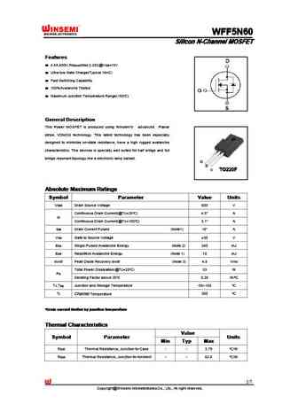
WFF5N60 WFF5N60 WFF5N60 WFF5N60 Silicon N-Channel MOSFET Silicon N-Channel MOSFET Silicon N-Channel MOSFET Silicon N-Channel MOSFET Features Features Features Features 4.5A,600V,RDS(on)(Max 2.2 )@VGS=10V Ultra-low Gate Charge(Typical 16nC) Fast Switching Capability 100%Avalanche Tested Maximum Junction Temperature Range(150 ) General Description General
wfp5n60.pdf
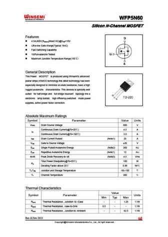
WFP5N60 WFP5N60 WFP5N60 WFP5N60 Silicon N-Channel MOSFET Silicon N-Channel MOSFET Silicon N-Channel MOSFET Silicon N-Channel MOSFET Features 4.5A,600V,R (Max2.5 )@V =10V DS(on) GS Ultra-low Gate charge(Typical 16nC) Fast Switching Capability 100%Avalanche Tested Maximum Junction Temperature Range(150 ) General Description This Power MOSFET is produced usi
bl25n60-w bl25n60-f.pdf
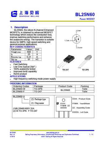
BL25N60 Power MOSFET 1 Description BL25N60, the silicon N-channel Enhanced MOSFETs, is obtained by advanced MOSFET technology which reduce the conduction loss, improve switching performance and enhance the avalanche energy. The transistor is suitable device for SMPS, high speed switching and general purpose applications. KEY CHARACTERISTICS Parameter Value Unit V 600
fhp15n60a fhf15n60a.pdf
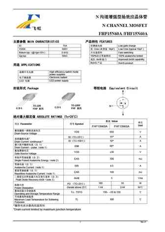
N N-CHANNEL MOSFET FHP15N60A /FHF15N60A MAIN CHARACTERISTICS FEATURES ID 15A Low gate charge VDSS 600V Crss ( 16pF) Low Crss (typical 16pF ) Rdson-typ @Vgs=10V 0.41 Fast switching Qg-typ 50nC 100% 100% avalanche tested dv/dt Improved dv
fht5n60d.pdf
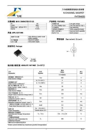
N N-CHANNEL MOSFET FHT5N60D MAIN CHARACTERISTICS FEATURES ID 5A Low gate charge VDSS 600V Crss ( 17pF) Low Crss (typical 17pF ) Rdson-typ @Vgs=10V 1.7 Fast switching Qg-typ 13.3nC 100% 100% avalanche tested dv/dt Improved dv/dt
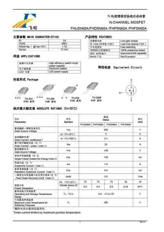
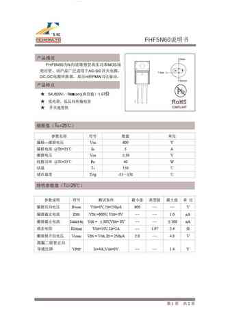
iqib75n60d3.pdf
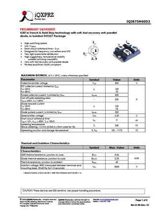
IQIB75N60D3 PRELIMINARY DATASHEET IGBT in Trench & Field Stop technology with soft, fast recovery anti-parallel diode, in Isolated SOT227 Package 1 High switching speed Low V CE(sat) Short circuit withstand time 5 us Designed for frequency converters and UPS Very tight parameter distribution 3 High ruggedness, temperature stability 2, 4 - parallel switch
iqib75n60a3.pdf
IQIB75N60A3 PRELIMINARY DATASHEET IGBT in Trench & Field Stop-technology in Isolated SOT227 Package Very high switching speed 1 Very low VCE(sat Short circuit withstand time 5 us Designed for frequency converters and UPS Very tight parameter distribution 3 High ruggedness, temperature stability - Parallel switching capability 2, 4 Pb-free lead finish
iqab75n60a1.pdf
IQAB75N60A1 PRELIMINARY DATASHEET IGBT Trench & Field Stop technology in TO247 Package Very high switching speed Very low V CE(sat) Short circuit withstand time - 5 s Designed for frequency converters and UPS Very tight parameter distribution High ruggedness, temperature stability Parallel switching capability Pb-free lead finish; RoHS comp
iqab75n60d1.pdf
IQAB75N60D1 PRELIMINARY DATASHEET IGBT in Trench & Field Stop technology with soft, fast recovery anti-parallel diode, in TO-247 Package Very high switching speed Very low V CE(sat) Short circuit withstand time - 5 s Designed for frequency converters and UPS Very tight parameter distribution High ruggedness, temperature stable Parallel switching capabilit
jfpc5n60c jffm5n60c.pdf
JFPC5N60C JFFM5N60C 600V N-Channel MOSFET General Description Features This Power MOSFET is produced using advanced - 4.5A , 600V, RDS(on)typ. = 2.0 @VGS = 10 V planar stripe DMOS technology. This advanced - Low gate charge technology has been especially tailored to minimize - High ruggedness on-state resistance, provide superior switching - Fast switching performance
kia5n60e.pdf
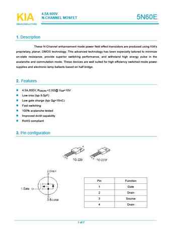
4.5A600V N-CHANNELMOSFET 5N60E KIA KIA KIA SEMICONDUCTORS SEMICONDUCTORS SEMICONDUCTORS 1.Description These N-Channel enhancement mode power field effect transistors are produced using KIA s proprietary, planar, DMOS technology. This advanced technology has been especially tailored to minimize on-state resistance, provide superior switching performance, and withstand high energy p
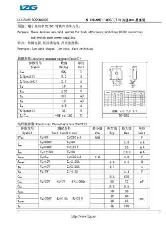
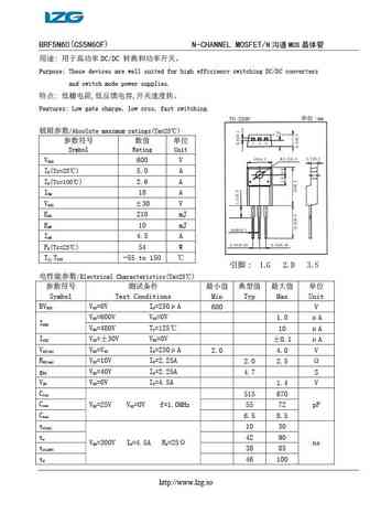
slp5n60c slf5n60c.pdf
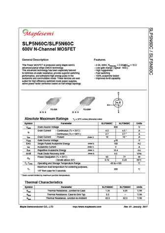
SLP5N60C/SLF5N60C 600V N-Channel MOSFET General Description Features This Power MOSFET is produced using Maple semi s - 4.5A, 600V, RDS(on)typ. = 2.0 @VGS = 10 V advanced planar stripe DMOS technology. - Low gate charge ( typical 16nC) This advanced technology has been especially tailored - High ruggedness to minimize on-state resistance, provide superior switching - Fast switching pe
ncep035n60ag.pdf
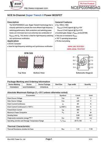
Pb Free Product http //www.ncepower.com NCEP035N60AG NCE N-Channel Super Trench II Power MOSFET Description General Features The NCEP035N60AG uses Super Trench II technology that is V =60V,I =90A DS D uniquely optimized to provide the most efficient high frequency R =2.8m (typical) @ V =10V DS(ON) GS switching performance. Both conduction and switching power R =3.5m (typical) @
ncep025n60.pdf

NCEP025N60, NCEP025N60D NCE N-Channel Super Trench II Power MOSFET Description The series of devices uses Super Trench II technology that is General Features uniquely optimized to provide the most efficient high frequency V =60V,I =190A DS D switching performance. Both conduction and switching power R =2.25m , typical @ V =10V DS(ON) GS losses are minimized due to an extremely
ncep025n60ag.pdf
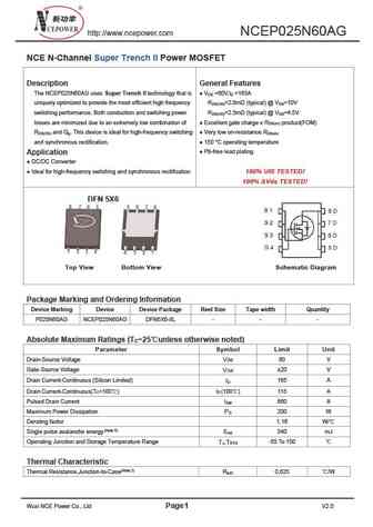
http //www.ncepower.com NCEP025N60AG NCE N-Channel Super Trench II Power MOSFET Description General Features The NCEP025N60AG uses Super Trench II technology that is V =60V,I =165A DS D uniquely optimized to provide the most efficient high frequency R =2.0m (typical) @ V =10V DS(ON) GS switching performance. Both conduction and switching power R =2.5m (typical) @ V =4.5V DS(ON)
ncep025n60 ncep025n60d.pdf
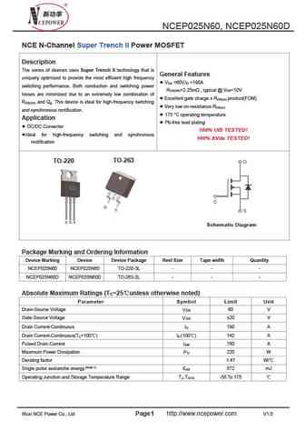
NCEP025N60, NCEP025N60D NCE N-Channel Super Trench II Power MOSFET Description The series of devices uses Super Trench II technology that is General Features uniquely optimized to provide the most efficient high frequency V =60V,I =190A DS D switching performance. Both conduction and switching power R =2.25m , typical @ V =10V DS(ON) GS losses are minimized due to an extremely
ncep055n60gu.pdf
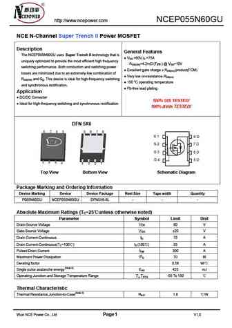
http //www.ncepower.com NCEP055N60GU NCE N-Channel Super Trench II Power MOSFET Description General Features The NCEP055N60GU uses Super Trench II technology that is VDS =60V,ID =75A uniquely optimized to provide the most efficient high frequency RDS(ON)=4.2m (Typ.) @ VGS=10V switching performance. Both conduction and switching power Excellent gate charge x RDS(on) p
ncep035n60k.pdf
http //www.ncepower.com NCEP035N60K NCE N-Channel Super Trench II Power MOSFET Description General Features The NCEP035N60K uses Super Trench II technology that is V =60V,I =130A DS D uniquely optimized to provide the most efficient high frequency R =2.8m (typical) @ V =10V DS(ON) GS switching performance. Both conduction and switching power Excellent gate charge x R produc
ncep035n60ak.pdf
http //www.ncepower.com NCEP035N60AK NCE N-Channel Super Trench II Power MOSFET Description General Features The NCEP035N60AK uses Super Trench II technology that is V =60V,I =130A DS D uniquely optimized to provide the most efficient high frequency R =2.8m (typical) @ V =10V DS(ON) GS switching performance. Both conduction and switching power R =3.5m (typical) @ V =4.5V DS(ON)
ncep015n60ll.pdf
NCEP015N60LL NCE N-Channel Super Trench II Power MOSFET Description The series of devices uses Super Trench II technology that is General Features uniquely optimized to provide the most efficient high frequency V =60V,I =340A DS D switching performance. Both conduction and switching power R =1.0m , typical @ V =10V DS(ON) GS losses are minimized due to an extremely low combinati
ncep025n60g.pdf
http //www.ncepower.com NCEP025N60G NCE N-Channel Super Trench II Power MOSFET Description General Features The NCEP025N60G uses Super Trench II technology that is VDS =60V,ID =165A uniquely optimized to provide the most efficient high frequency RDS(ON)=2.2m (typical) @ VGS=10V switching performance. Both conduction and switching power Excellent gate charge x RDS(on)
nceap025n60ag.pdf
http //www.ncepower.com NCEAP025N60AG NCE Automotive N-Channel Super Trench II Power MOSFET Description General Features The NCEAP025N60AG uses Super Trench II technology that is V =60V,I =185A (Silicon Limited) DS D uniquely optimized to provide the most efficient high frequency R =2.0m (typical) @ V =10V DS(ON) GS switching performance. Both conduction and switching power R =2.5m
ncep025n60d.pdf

NCEP025N60, NCEP025N60D NCE N-Channel Super Trench II Power MOSFET Description The series of devices uses Super Trench II technology that is General Features uniquely optimized to provide the most efficient high frequency V =60V,I =190A DS D switching performance. Both conduction and switching power R =2.25m , typical @ V =10V DS(ON) GS losses are minimized due to an extremely
swt45n60k2f.pdf
SW45N60K2F N-channel Enhanced mode TO-247 MOSFET TO-247 BVDSS 600V Features ID 45A High ruggedness RDS(ON) 65m Low RDS(ON) (Typ 65m )@VGS=10V Low Gate Charge (Typ 74nC) 2 Improved dv/dt Capability 1 100% Avalanche Tested 2 1 3 Application Charger, LED , UPS 1. Gate 2. Drain 3. Source 3 General Description This power MOS
swf5n60d swmn5n60d.pdf
SW5N60D N-channel Enhanced mode TO-220F/TO-220SF MOSFET Features TO-220F TO-220SF BVDSS 600V ID 5A High ruggedness Low RDS(ON) (Typ1.9 )@VGS=10V RDS(ON) 1.9 Low Gate Charge (Typ17nC) Improved dv/dt Capability 2 1 1 100% Avalanche Tested 2 2 3 3 Application DC-DC,LED 1 1. Gate 2. Drain 3. Source 3 General Description
swt45n60k2.pdf
SW45N60K2 N-channel Enhanced mode TO-247 MOSFET TO-247 BVDSS 600V Features ID 45A High ruggedness RDS(ON) 60m Low RDS(ON) (Typ 60m )@VGS=10V Low Gate Charge (Typ 74nC) 2 Improved dv/dt Capability 1 100% Avalanche Tested 2 1 3 Application Charger, LED , UPS 1. Gate 2. Drain 3. Source 3 General Description This power MOSF
hfs5n60u.pdf
May 2012 BVDSS = 600 V RDS(on) typ HFS5N60U ID = 4.5 A 600V N-Channel MOSFET TO-220F FEATURES Originative New Design Superior Avalanche Rugged Technology 1 2 3 Robust Gate Oxide Technology 1.Gate 2. Drain 3. Source Very Low Intrinsic Capacitances Excellent Switching Characteristics Unrivalled Gate Charge 10.5 nC (Typ.) Extended Safe Operating Area
hfd5n60s.pdf
Sep 2009 BVDSS = 600 V RDS(on) typ = 2.0 HFD5N60S / HFU5N60S ID = 4.3 A 600V N-Channel MOSFET D-PAK I-PAK 2 2 FEATURES 1 1 3 2 3 Originative New Design HFD5N60S HFU5N60S Superior Avalanche Rugged Technology 1.Gate 2. Drain 3. Source Robust Gate Oxide Technology Very Low Intrinsic Capacitances Excellent Switching Characteristics Unrivalled Gate Charge 10.5 nC (Typ
hfp5n60f hfs5n60f.pdf
Oct 2016 HFP5N60F / HFS5N60F 600V N-Channel MOSFET Features Key Parameters Parameter Value Unit Originative New Design BVDSS 600 V Very Low Intrinsic Capacitances ID 5A Excellent Switching Characteristics RDS(on), Typ 1.8 100% Avalanche Tested Qg, Typ 12.5 nC RoHS Compliant HFP5N60F HFS5N60F Symbol TO-220 TO-220F S S D D G G Absolute Maximum Ratings TC=25 unle
hfd5n60s hfu5n60s.pdf
June 2015 BVDSS = 600 V RDS(on) typ HFD5N60S / HFU5N60S ID = 4.3 A 600V N-Channel MOSFET D-PAK I-PAK 2 FEATURES 1 1 3 2 3 Originative New Design HFD5N60S HFU5N60S Superior Avalanche Rugged Technology 1.Gate 2. Drain 3. Source Robust Gate Oxide Technology Very Low Intrinsic Capacitances Excellent Switching Characteristics Unrivalled Gate Charge 10.5 nC
hfw5n60s.pdf

Sep 2009 BVDSS = 600 V RDS(on) typ HFW5N60S / HFI5N60S ID = 4.5 A 600V N-Channel MOSFET D2-PAK I2-PAK FEATURES Originative New Design HFW5N60S HFI5N60S Superior Avalanche Rugged Technology 1.Gate 2. Drain 3. Source Robust Gate Oxide Technology Very Low Intrinsic Capacitances Excellent Switching Characteristics Unrivalled Gate Charge 10.5 nC (Typ.) Extended Saf
hfd5n60u.pdf
Jan 2014 BVDSS = 600 V RDS(on) typ = 2.0 HFD5N60U / HFU5N60U ID = 3.6 A 600V N-Channel MOSFET D-PAK I-PAK FEATURES 2 1 Originative New Design 1 3 2 3 Superior Avalanche Rugged Technology HFD5N60U HFU5N60U Robust Gate Oxide Technology 1.Gate 2. Drain 3. Source Very Low Intrinsic Capacitances Excellent Switching Characteristics Unrivalled Gate Charge 10.5 nC
hfp5n60u.pdf
May 2012 BVDSS = 600 V RDS(on) typ HFP5N60U ID = 4.5 A 600V N-Channel MOSFET TO-220 FEATURES Originative New Design Superior Avalanche Rugged Technology 1 2 3 Robust Gate Oxide Technology 1.Gate 2. Drain 3. Source Very Low Intrinsic Capacitances Excellent Switching Characteristics Unrivalled Gate Charge 10.5 nC (Typ.) Extended Safe Operating Area L
hfd5n60u hfu5n60u.pdf

June 2015 BVDSS = 600 V RDS(on) typ = 2.0 HFD5N60U / HFU5N60U ID = 3.6 A 600V N-Channel MOSFET D-PAK I-PAK FEATURES 2 1 Originative New Design 1 3 2 3 Superior Avalanche Rugged Technology HFD5N60U HFU5N60U Robust Gate Oxide Technology 1.Gate 2. Drain 3. Source Very Low Intrinsic Capacitances Excellent Switching Characteristics Unrivalled Gate Charge 10.5 nC
hfs5n60s.pdf
Aug 2007 BVDSS = 600 V RDS(on) typ HFS5N60S ID = 4.5 A 600V N-Channel MOSFET TO-220F FEATURES 1 Originative New Design 2 3 Superior Avalanche Rugged Technology 1.Gate 2. Drain 3. Source Robust Gate Oxide Technology Very Low Intrinsic Capacitances Excellent Switching Characteristics Unrivalled Gate Charge 10.5 nC (Typ.) Extended Safe Operating Area
hfw5n60s hfi5n60s.pdf

Sep 2009 BVDSS = 600 V RDS(on) typ HFW5N60S / HFI5N60S ID = 4.5 A 600V N-Channel MOSFET D2-PAK I2-PAK FEATURES Originative New Design HFW5N60S HFI5N60S Superior Avalanche Rugged Technology 1.Gate 2. Drain 3. Source Robust Gate Oxide Technology Very Low Intrinsic Capacitances Excellent Switching Characteristics Unrivalled Gate Charge 10.5 nC (Typ.) Extended Saf
hfp5n60s.pdf
Aug 2007 BVDSS = 600 V RDS(on) typ HFP5N60S ID = 4.5 A 600V N-Channel MOSFET TO-220 FEATURES Originative New Design 1 2 3 Superior Avalanche Rugged Technology 1.Gate 2. Drain 3. Source Robust Gate Oxide Technology Very Low Intrinsic Capacitances Excellent Switching Characteristics Unrivalled Gate Charge 10.5 nC (Typ.) Extended Safe Operating Area Lower RDS(
hfu5n60f hfd5n60f.pdf
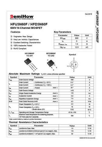
Oct 2016 HFU5N60F / HFD5N60F 600V N-Channel MOSFET Features Key Parameters Parameter Value Unit Originative New Design BVDSS 600 V Very Low Intrinsic Capacitances ID 5A Excellent Switching Characteristics RDS(on), Typ 1.8 100% Avalanche Tested Qg, Typ 12.5 nC RoHS Compliant HFU5N60F HFD5N60F Symbol TO-251 TO-252 D S S D G G Absolute Maximum Ratings TC=25 unles
wvm15n60.pdf
Shaanxi Qunli Electric Co., Ltd Add. No. 1 Qunli Road,Baoji City,Shaanxi,China WVM15N60 Power MOSFET(N-channel) Transistor Features 1. It s voltage control component with good input impedance, small starting power dissipation, wide area of safe operation, good temperature stability. 2. Implementation of standards QZJ840611 3. Use for high speed switch, circuit of power source co
msu5n60.pdf
600V/4.5A POWER MOSFET (N-Channel) MSU5N60 600V/4.5A Power MOSFET (N-Channel) General Description MSU5N60 is a N-Channel enhancement mode power MOSFET with advanced TO-220 technology. It is designed to have better characteristics, such as fast switching time, low gate charge, minimized on-state resistance and withstanding high energy pulse in the avalanche and commutati
msk7d5n60f msk7d5n60t.pdf
600V/7.5A N-Channel MOSFET MSK7D5N60T/F 600V/7.5A N-Channel MOSFET General Description Fast switching time Low on resistance, low gate charge Excellent avalanche characteristics Suitable for active power factor correction Suitable for switching mode power supplies TO-220 Features VDSS=600V, ID=7.5A; Low Drain-Source ON Resistance RDS(ON) =
msk4d5n60f msk4d5n60t.pdf
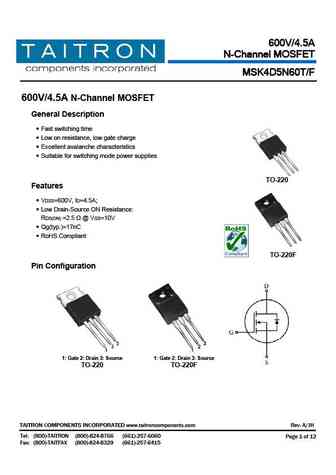
600V/4.5A N-Channel MOSFET MSK4D5N60T/F 600V/4.5A N-Channel MOSFET General Description Fast switching time Low on resistance, low gate charge Excellent avalanche characteristics Suitable for switching mode power supplies TO-220 Features VDSS=600V, ID=4.5A; Low Drain-Source ON Resistance RDS(ON) =2.5 @ VGS=10V Qg(typ.)=17nC RoHS C
tsu45n60.pdf
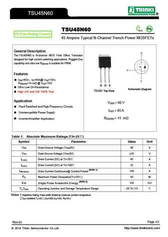
TSU45N60 Table 2. Thermal Characteristic Symbol Parameter Value Unit R JC Thermal Resistance,Junction-to-Case 2.7 /W Table 3. Electrical Characteristics (TA=25 unless otherwise noted) Symbol Parameter Conditions Min Typ Max Unit On/Off States BVDSS Drain-Source Breakdown Voltage VGS=0V ID=250 A 60 V IDSS Zero Gate Voltage Drain Current(Tc=25 ) VDS=60V,VGS=0V 1 A
tmp5n60az tmpf5n60az.pdf
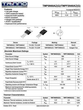
TMP5N60AZ(G)/TMPF5N60AZ(G) Features N-channel MOSFET Low gate charge BVDSS ID RDS(on) 100% avalanche tested 600V 4.2A
tmd5n60z tmu5n60z.pdf
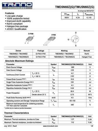
TMD5N60Z(G)/TMU5N60Z(G) N-channel MOSFET Features BVDSS ID RDS(on)MAX Low gate charge 600V 4.2A
tmp5n60z tmpf5n60z.pdf
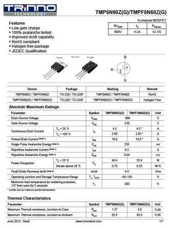
TMP5N60Z(G)/TMPF5N60Z(G) N-channel MOSFET Features BVDSS ID RDS(on) Low gate charge 600V 4.2A
tgpf15n60fdr.pdf
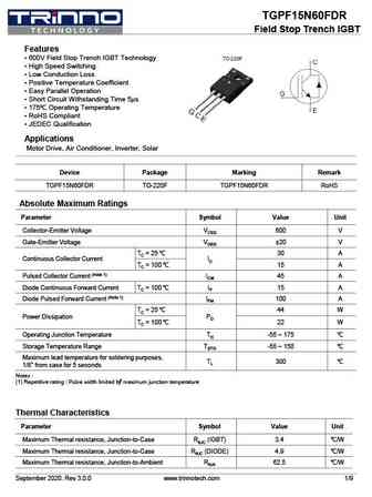
TGPF15N60FDR Field Stop Trench IGBT Features 600V Field Stop Trench IGBT Technology High Speed Switching Low Conduction Loss Positive Temperature Coefficient Easy Parallel Operation Short Circuit Withstanding Time 5 s 175 Operating Temperature RoHS Compliant JEDEC Qualification Applications Motor Drive, Air Conditioner, Inverter, Solar Devic
tmd5n60az tmu5n60az.pdf
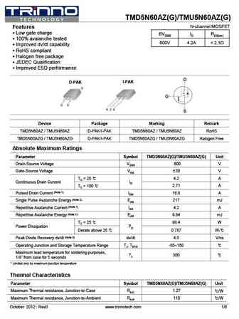
TMD5N60AZ(G)/TMU5N60AZ(G) N-channel MOSFET Features Low gate charge BVDSS ID RDS(on) 100% avalanche tested 600V 4.2A
tsp5n60m tsf5n60m.pdf
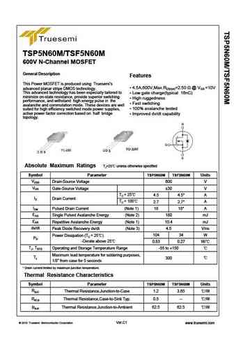
TSP5N60M/TSF5N60M 600V N-Channel MOSFET General Description Features This Power MOSFET is produced using Truesemi s 4.5A,600V,Max.RDS(on)=2.50 @ VGS =10V advanced planar stripe DMOS technology. This advanced technology has been especially tailored to Low gate charge(typical 16nC) minimize on-state resistance, provide superior switching High ruggedness performance, an
tsd5n60m tsu5n60m.pdf
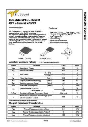
TSD5N60M/TSU5N60M 600V N-Channel MOSFET General Description Features This Power MOSFET is produced using Truesemi s 4.5A,600V,Max.RDS(on)=2.5 @ VGS =10V advanced planar stripe DMOS technology. This advanced technology has been especially tailored to Low gate charge(typical 12nC) minimize on-state resistance, provide superior switching High ruggedness performance, and
wml15n60c4 wmk15n60c4 wmm15n60c4 wmn15n60c4 wmp15n60c4 wmo15n60c4.pdf
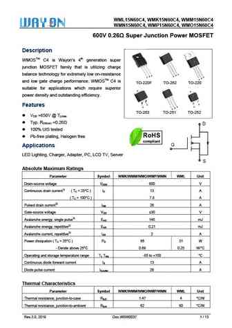
WML1 MM15N60C 15N60C4, WMK15N60C4, WM C4 WMN15N60C4, WMP15N60C4, WM C4 MO15N60C 600V n Power MOSFET V 0.26 Super Junction Descrip ption WMOSTM C4 is Wa 4th generation super ayon s n junction MOSFET fa that is utilizing charge M amily S balance te or extremely esistance echnology fo y low on-re D S D G G G S D G and low ga charge performanc WMOSTM C4
cs5n60a8h.pdf
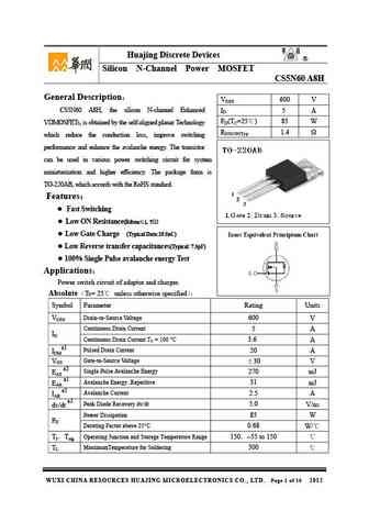
Huajing Discrete Devices R Silicon N-Channel Power MOSFET CS5N60 A8H General Description VDSS 600 V CS5N60 A8H, the silicon N-channel Enhanced ID 5 A PD(TC=25 ) 85 W VDMOSFETs, is obtained by the self-aligned planar Technology RDS(ON)Typ 1.4 which reduce the conduction loss, improve switching performance and enhance the avalanche energy. The transistor ca
cs5n60a4h.pdf
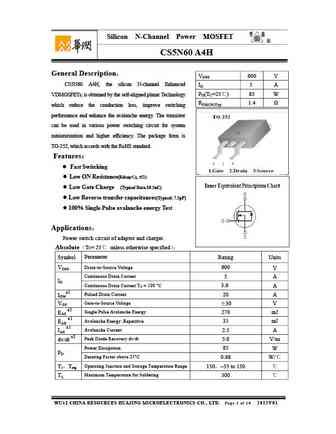
Silicon N-Channel Power MOSFET R CS5N60 A4H General Description VDSS 600 V CS5N60 A4H, the silicon N-channel Enhanced ID 5 A PD(TC=25 ) 85 W VDMOSFETs, is obtained by the self-aligned planar Technology RDS(ON)Typ 1.4 which reduce the conduction loss, improve switching performance and enhance the avalanche energy. The transistor can be used in various power
cs5n60fa9hd.pdf
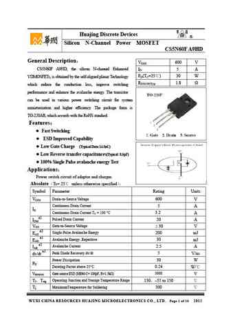
Huajing Discrete Devices R Silicon N-Channel Power MOSFET CS5N60F A9HD General Description VDSS 600 V CS5N60F A9HD, the silicon N-channel Enhanced ID 5 A PD(TC=25 ) 30 W VDMOSFETs, is obtained by the self-aligned planar Technology RDS(ON)Typ 1.8 which reduce the conduction loss, improve switching performance and enhance the avalanche energy. The transistor
bt15n60a9f.pdf

Silicon FS Planar IGBT R BT15N60A9F General Description VCES 600 V Using HUAJING's proprietary Planar design and advanced FS IC 15 A technology, the 600V FSIGBT offers superior conduction and switching Ptot TC=25 25 W performances, high avalanche ruggedness and easy parallel operation. VCE(SAT) 2.1 V Features FS Planar Technology, Positive temperature coeff
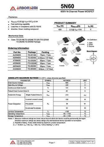
fir5n60fg.pdf
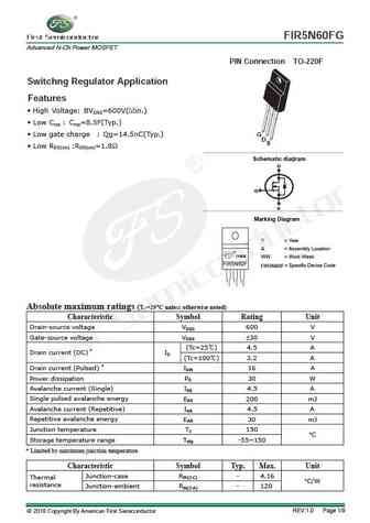
FIR5N60FG Advanced N-Ch Power MOSFET PIN Connection TO-220F Switchng Regulator Application Features High Voltage BVDSS=600V(Min.) Low Crss Crss=8.5F(Typ.) Low gate charge Qg=14.5nC(Typ.) G D S Low RDS(on) RDS(on)=1.8 g Schematic dia ram D G S Marking Diagram Y = Year A = Assembly Location YAWW WW = Work Week FIR5N60F FIR5N60F = Specific D
smt5n60.pdf
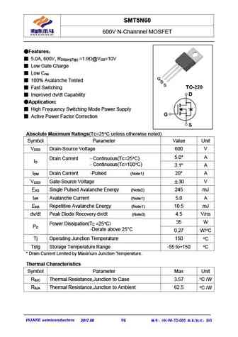
SMT5N60 600V N-Channnel MOSFET Features 5.0A, 600V, R =1.9 @V =10V DS(on)(Typ) GS Low Gate Charge Low C rss 100% Avalanche Tested Fast Switching Improved dv/dt Capability Application High Frequency Switching Mode Power Supply Active Power Factor Correction Absolute Maximum Ratings(Tc=25 C unless otherwise noted) Symbol Parameter Value
smf5n60.pdf
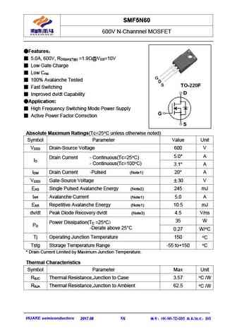
SMF5N60 600V N-Channnel MOSFET Features 5.0A, 600V, R =1.9 @V =10V DS(on)(Typ) GS Low Gate Charge Low C rss 100% Avalanche Tested Fast Switching Improved dv/dt Capability Application High Frequency Switching Mode Power Supply Active Power Factor Correction Absolute Maximum Ratings(Tc=25 C unless otherwise noted) Symbol Parameter Value
jmpc25n60bj.pdf
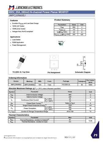
600V, 25A, 282m N-channel Power Planar MOSFET JMPC25N60BJ Product Summary Features Excellent RDS(ON) and Low Gate Charge Parameters Value Unit 100% UIS Tested VDSS 600 V 100% Vds Tested VGS(th)_Typ 3.0 V Halogen-free; RoHS-compliant ID(@VGS=10V) 25 A RDS(ON)_Typ(@VGS=10V 282 mW Applications Load Switch PWM Application Power Management D G S
si5n60.pdf
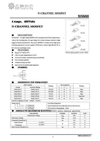
N-CHANNEL MOSFET SI5N60 4 Amps 600Volts 4 Amps 600Volts 4 Amps 600Volts 4 Amps 600Volts N-CHANNEL MOSFET N-CHANNEL MOSFET N-CHANNEL MOSFET N-CHANNEL MOSFET DESCRIPTION The SI5N60 is a high voltage MOSFET and is designed to have better characteristics , such as fast switching time, low gate charge, low on-state resistance and have a high rugged avalanche characteristics. This
sig25n60f sig25n60p sig25n60w sig25n60b.pdf
SUPER-SEMI Super Junction Insulated Gate Bipolar Transistor 600V Trench and Super Junction IGBT SIG25N60* Rev. 0.3 Sep.2021 www.supersemi.com.cn SIG25N60F/SIG25N60P/SIG25N60W/SIG25N60B 600V Trench and Super Junction IGBT General Description Super-Semi Trench and Super Junction IGBTs, VCE 600 V designed according to the superjunction (SJ) IC 25 A principle. The SJ-IGBT series pr
dgf15n60ctl.pdf
RoHS DGF15N60CTL COMPLIANT IGBT Discrete V 600 V CE I 15 A C V I = A 1.65 V CE(SAT) C 15 Applications Soft switchingapplications Circuit Airconditioning Motor driveinverter Features High speed smooth switching device for hard & soft switching Maximum junction temperature 175 Positive temperature coefficient High ruggedness,
dgf15n60ctl0.pdf
RoHS DGF15N60CTL0 COMPLIANT IGBT Discrete V 600 V CE I 15 A C V I = A 1.65 V CE(SAT) C 15 Applications Circuit Soft switching applications Air conditioning Motor drive inverter Features High speed smooth switching device for hard & soft switching Maximum junction temperature 175 Positive temperature coefficient High ruggedness
dgp15n60ctl.pdf
RoHS DGP15N60CTL COMPLIANT IGBT Discrete V 600 V CE I 15 A C V I = A 1.65 V CE(SAT) C 15 Applications Circuit Soft switchingapplications Airconditioning Motor driveinverter Features High speed smooth switching device for hard & soft switching Maximum junction temperature 175 Positive temperature coefficient High ruggedness, t
hms15n60 hms15n60f hms15n60d.pdf
HM 15N60D, HM 15N60, HM 15N60F N-Channel Super Junction Power MOSFET General Description The series of devices use advanced super junction 600 V VDS@Tjmax technology and design to provide excellent RDS(ON) with low RDS(ON)MAX 60 gate charge. This super junction MOSFET fits the industry s ID 1 A AC-DC SMPS requirements for PFC, AC/DC power conversion, and
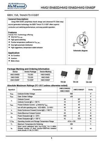
hm5n60k hm5n60i.pdf
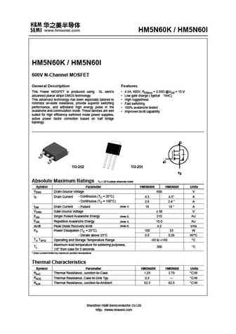
HM5N60K / HM5N60I HM5N60K / HM5N60I 600V N-Channel MOSFET General Description Features This Power MOSFET is produced using SL semi s 4.5A, 600V, RDS(on) = 2.50 @VGS = 10 V advanced planar stripe DMOS technology. Low gate charge ( typical 16nC) This advanced technology has been especially tailored to High ruggedness minimize on-state resistance, provide superior switchin
hm5n60.pdf
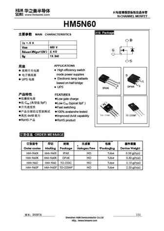
N R N-CHANNEL MOSFET HM5N60 Package MAIN CHARACTERISTICS .0 A ID 5 600 V VDSS Rdson 2.4 @Vgs=10V 13.3nC Qg APPLICATIONS High efficiency switch mode power supplies Electronic lamp ballasts UPS based on half bridge UPS
hm5n60 hm5n60f.pdf
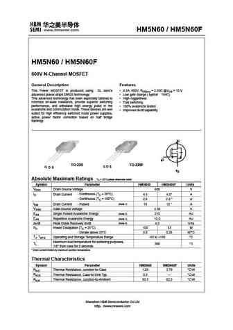
HM5N60 / HM5N60F HM5N60 / HM5N60F 600V N-Channel MOSFET General Description Features This Power MOSFET is produced using SL semi s 4.5A, 600V, RDS(on) = 2.50 @VGS = 10 V advanced planar stripe DMOS technology. Low gate charge ( typical 16nC) This advanced technology has been especially tailored to High ruggedness minimize on-state resistance, provide superior switching
hms15n60a.pdf
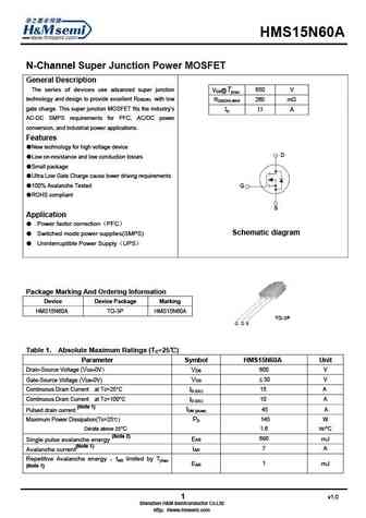
HMS15N60A N-Channel Super Junction Power MOSFET General Description The series of devices use advanced super junction 650 V VDS@Tjmax technology and design to provide excellent RDS(ON) with low RDS(ON) MAX 0 m gate charge. This super junction MOSFET fits the industry s ID 1 A AC-DC SMPS requirements for PFC, AC/DC power conversion, and industrial power appl
h5n60p h5n60f.pdf
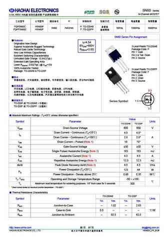
5N60 Series N-Channel MOSFET 4.5A, 600V, N H FQP5N60C H5N60P P TO-220AB 5N60 HAOHAI 50Pcs 1000Pcs 5000Pcs FQPF5N60C H5N60F F TO-220FP 5N60 Series Pin Assignment Features ID=4.5A Originative New De
h5n60u h5n60d.pdf
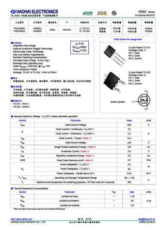
5N60 Series N-Channel MOSFET 5A, 600V, N H FQU5N60C H5N60U U TO-251 80 / 4Kpcs/ 24Kpcs 5N60 HAOHAI FQD5N60C H5N60D D TO-252 25Kpcs 2.5K/ 5Kpcs/ 5N60 Series Pin Assignment Features ID=3.6A Ori
mcu05n60a.pdf
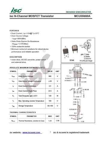
isc N-Channel MOSFET Transistor MCU05N60A FEATURES Drain Current I = 4.5A@ T =25 D C Drain Source Voltage V = 600V(Min) DSS Static Drain-Source On-Resistance R = 2.5 (Max) DS(on) 100% avalanche tested Minimum Lot-to-Lot variations for robust device performance and reliable operation DESCRIPTION motor drive, DC-DC converter, power switch and solenoid drive.
aot5n60.pdf
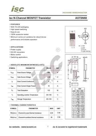
isc N-Channel MOSFET Transistor AOT5N60 FEATURES With TO-220 packaging High speed switching Easy to use 100% avalanche tested Minimum Lot-to-Lot variations for robust device performance and reliable operation APPLICATIONS Power supply DC-DC converters Motor control Switching applications ABSOLUTE MAXIMUM RATINGS(T =25 ) a SYMBOL PARAMETER VALUE UNIT V D
spp15n60cfd.pdf
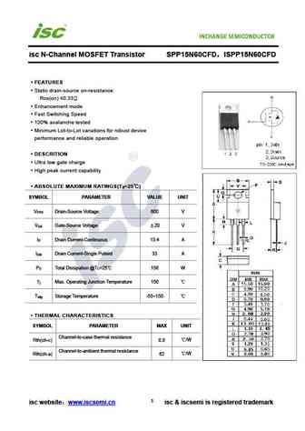
isc N-Channel MOSFET Transistor SPP15N60CFD ISPP15N60CFD FEATURES Static drain-source on-resistance RDS(on) 0.33 Enhancement mode Fast Switching Speed 100% avalanche tested Minimum Lot-to-Lot variations for robust device performance and reliable operation DESCRITION Ultra low gate charge High peak current capability ABSOLUTE MAXIMUM RATINGS(T =25 ) a
spp15n60c3.pdf
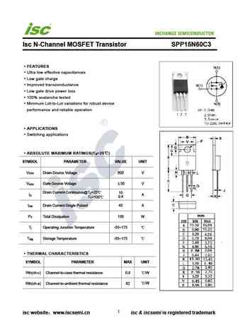
INCHANGE Semiconductor Isc N-Channel MOSFET Transistor SPP15N60C3 FEATURES Ultra low effective capacitances Low gate charge Improved transconductance Low gate drive power loss 100% avalanche tested Minimum Lot-to-Lot variations for robust device performance and reliable operation APPLICATIONS Switching applications ABSOLUTE MAXIMUM RATINGS(T =25 ) a SYMBOL PA
fmh35n60s1fd.pdf
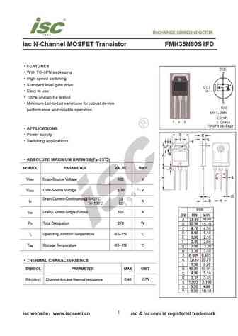
isc N-Channel MOSFET Transistor FMH35N60S1FD FEATURES With TO-3PN packaging High speed switching Standard level gate drive Easy to use 100% avalanche tested Minimum Lot-to-Lot variations for robust device performance and reliable operation APPLICATIONS Power supply Switching applications ABSOLUTE MAXIMUM RATINGS(T =25 ) a SYMBOL PARAMETER VALUE UNIT V Drai
spa15n60c3.pdf
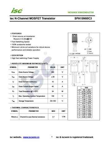
isc N-Channel MOSFET Transistor SPA15N60C3 FEATURES Drain-source on-resistance RDS(on) 0.28 @10V Fast Switching Speed 100% avalanche tested Minimum Lot-to-Lot variations for robust device performance and reliable operation DESCRITION High fast switching Power Supply ABSOLUTE MAXIMUM RATINGS(T =25 ) a SYMBOL PARAMETER VALUE UNIT V Drain-Source Voltage 600 V
spw15n60cfd.pdf
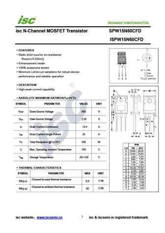
INCHANGE Semiconductor isc N-Channel MOSFET Transistor SPW15N60CFD ISPW15N60CFD FEATURES Static drain-source on-resistance RDS(on) 330m Enhancement mode 100% avalanche tested Minimum Lot-to-Lot variations for robust device performance and reliable operation DESCRITION High peak current capability ABSOLUTE MAXIMUM RATINGS(T =25 ) a SYMBOL PARAMETER VALUE UN
spa15n60cfd.pdf
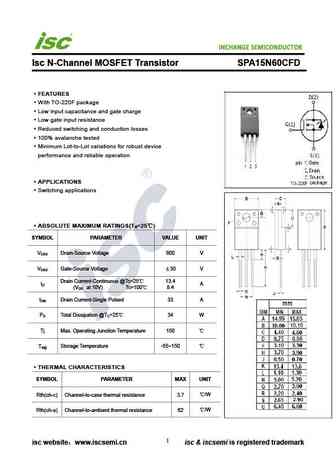
INCHANGE Semiconductor Isc N-Channel MOSFET Transistor SPA15N60CFD FEATURES With TO-220F package Low input capacitance and gate charge Low gate input resistance Reduced switching and conduction losses 100% avalanche tested Minimum Lot-to-Lot variations for robust device performance and reliable operation APPLICATIONS Switching applications ABSOLUTE MAXIMUM RATING
fcp165n60e.pdf
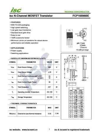
isc N-Channel MOSFET Transistor FCP165N60E FEATURES With TO-220 packaging High speed switching Low gate input resistance Standard level gate drive Easy to use 100% avalanche tested Minimum Lot-to-Lot variations for robust device performance and reliable operation APPLICATIONS Power supply Switching applications ABSOLUTE MAXIMUM RATINGS(T =25 ) a SYMBOL P
spw15n60c3.pdf
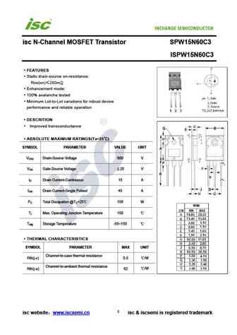
isc N-Channel MOSFET Transistor SPW15N60C3 ISPW15N60C3 FEATURES Static drain-source on-resistance RDS(on) 280m Enhancement mode 100% avalanche tested Minimum Lot-to-Lot variations for robust device performance and reliable operation DESCRITION Improved transconductance ABSOLUTE MAXIMUM RATINGS(T =25 ) a SYMBOL PARAMETER VALUE UNIT V Drain-Source Voltage 6
spw35n60cfd.pdf
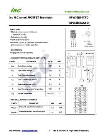
isc N-Channel MOSFET Transistor SPW35N60CFD ISPW35N60CFD FEATURES Static drain-source on-resistance RDS(on) 118m Enhancement mode 100% avalanche tested Minimum Lot-to-Lot variations for robust device performance and reliable operation DESCRITION High peak current capability ABSOLUTE MAXIMUM RATINGS(T =25 ) a SYMBOL PARAMETER VALUE UNIT V Drain-Source Volta
spw35n60c3.pdf
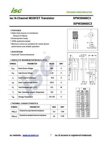
isc N-Channel MOSFET Transistor SPW35N60C3 ISPW35N60C3 FEATURES Static drain-source on-resistance RDS(on) 100m Enhancement mode 100% avalanche tested Minimum Lot-to-Lot variations for robust device performance and reliable operation DESCRITION Improved Transconductance ABSOLUTE MAXIMUM RATINGS(T =25 ) a SYMBOL PARAMETER VALUE UNIT V Drain-Source Voltage 60
15n60.pdf
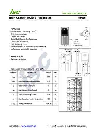
isc N-Channel MOSFET Transistor 15N60 FEATURES Drain Current I = 15A@ T =25 D C Drain Source Voltage V = 600V(Min) DSS Static Drain-Source On-Resistance R = 0.44 (Max) DS(on) High Switching Speed Minimum Lot-to-Lot variations for robust device performance and reliable operation APPLICATIONS Switching regulators ABSOLUTE MAXIMUM RATINGS(T =25 ) a SYMB
fcp125n60e.pdf

isc N-Channel MOSFET Transistor FCP125N60E FEATURES With TO-220 packaging High speed switching Low gate input resistance Standard level gate drive Easy to use 100% avalanche tested Minimum Lot-to-Lot variations for robust device performance and reliable operation APPLICATIONS Power supply Switching applications ABSOLUTE MAXIMUM RATINGS(T =25 ) a SYMBOL P
irfp15n60l.pdf
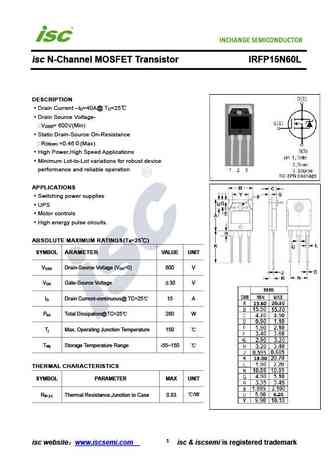
isc N-Channel MOSFET Transistor IRFP15N60L DESCRIPTION Drain Current I =40A@ T =25 D C Drain Source Voltage- V = 600V(Min) DSS Static Drain-Source On-Resistance R =0.46 (Max) DS(on) High Power,High Speed Applications Minimum Lot-to-Lot variations for robust device performance and reliable operation APPLICATIONS Switching power supplies UPS Motor contro
Другие IGBT... 3N65Z, 3N65K, 4N65, 4N65Z, 4N65K, 5N65, 5N65K, 6N65, AO4468, 6N60, 6N60Z, 7N60A, 7N60, 7N60Z, 7N60K, 8N60, 10N60
Параметры MOSFET. Взаимосвязь и компромиссы
🌐 : EN ES РУ

Список транзисторов
Обновления
MOSFET: CS95118 | CS85105A | CS75N45 | CS72N12 | CS55N50 | CS48N75A | CS40N27 | MSQ60P04D | MSQ40P07D | MSQ30P40D | MSQ30P15 | MSQ30P07D | MSQ100N03D | MSHM60P14 | MSHM40N085 | MSHM30N46
Popular searches
cs840f | 2n3053 equivalent | 2n3569 | 2sd667 | 2sc1111 | bc239 transistor equivalent | 3sk41 | 2sc2240 transistor