6N60 datasheet, аналоги, основные параметры
Наименование производителя: 6N60 📄📄
Тип транзистора: MOSFET
Полярность: N
Предельные значения
Pd ⓘ - Максимальная рассеиваемая мощность: 125 W
|Vds|ⓘ - Максимально допустимое напряжение сток-исток: 600 V
|Vgs|ⓘ - Максимально допустимое напряжение затвор-исток: 30 V
|Id| ⓘ - Максимально допустимый постоянный ток стока: 6.2 A
Tj ⓘ - Максимальная температура канала: 150 °C
Электрические характеристики
tr ⓘ - Время нарастания: 70 ns
Cossⓘ - Выходная емкость: 95 pf
RDSonⓘ - Сопротивление сток-исток открытого транзистора: 1 Ohm
📄📄 Копировать
Аналог (замена) для 6N60
- подборⓘ MOSFET транзистора по параметрам
6N60 даташит
6n60.pdf
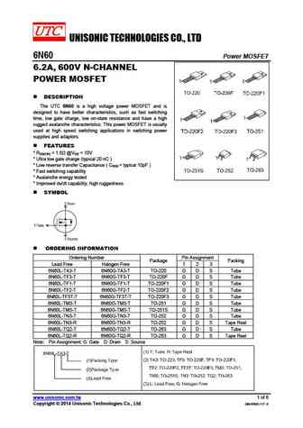
UNISONIC TECHNOLOGIES CO., LTD 6N60 Power MOSFET 6.2A, 600V N-CHANNEL POWER MOSFET DESCRIPTION The UTC 6N60 is a high voltage power MOSFET and is designed to have better characteristics, such as fast switching time, low gate charge, low on-state resistance and have a high rugged avalanche characteristics. This power MOSFET is usually used at high speed switching applicatio
h06n60u h06n60e h06n60f.pdf
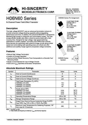
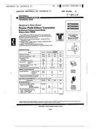
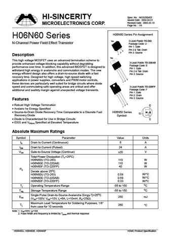
Spec. No. MOS200402 HI-SINCERITY Issued Date 2004.04.01 Revised Date 2005.03.10 MICROELECTRONICS CORP. Page No. 1/6 H06N60 Series Pin Assignment H06N60 Series Tab 3-Lead Plastic TO-263 N-Channel Power Field Effect Transistor Package Code U Pin 1 Gate Pin 2 & Tab Drain 3 2 Pin 3 Source 1 Description Tab This high voltage MOSFET uses an advanced termination scheme t
sgs6n60ufd.pdf
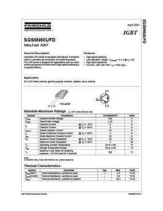
April 2001 IGBT SGS6N60UFD Ultra-Fast IGBT General Description Features Fairchild's UFD series of Insulated Gate Bipolar Transistors High speed switching (IGBTs) provides low conduction and switching losses. Low saturation voltage VCE(sat) = 2.1 V @ IC = 3A The UFD series is designed for applications such as motor High input impedance control and general inverters where
sgs6n60uf.pdf
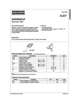
April 2001 IGBT SGS6N60UF Ultra-Fast IGBT General Description Features Fairchild's UF series of Insulated Gate Bipolar Transistors High speed switching (IGBTs) provides low conduction and switching losses. Low saturation voltage VCE(sat) = 2.1 V @ IC = 3A The UF series is designed for applications such as motor High input impedance control and general inverters where hig
ndf06n60z ndp06n60z.pdf
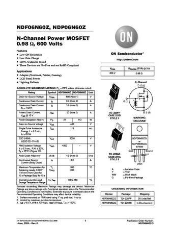
NDF06N60Z, NDP06N60Z N-Channel Power MOSFET 0.98 W, 600 Volts Features Low ON Resistance Low Gate Charge http //onsemi.com 100% Avalanche Tested These Devices are Pb-Free and are RoHS Compliant VDSS RDS(ON) (TYP) @ 3 A Applications 600 V 0.98 Adapter (Notebook, Printer, Gaming) LCD Panel Power N-Channel Lighting Ballasts D (2) ABSOLUTE MAXIMUM RA
mtb6n60e1rev1.pdf
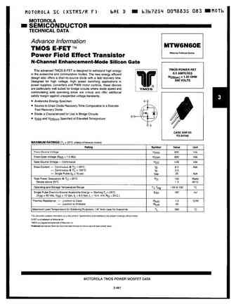
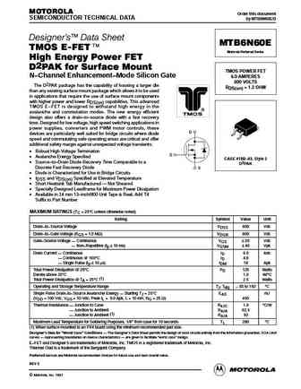
MOTOROLA Order this document SEMICONDUCTOR TECHNICAL DATA by MTB6N60E1/D Product Preview MTB6N60E1 TMOS E-FET. Motorola Preferred Device High Energy Power FET D2PAK-SL Straight Lead TMOS POWER FET N Channel Enhancement Mode Silicon Gate 6.0 AMPERES 600 VOLTS This advanced TMOS E FET is designed to withstand high RDS(on) = 1.2 OHM energy in the avalanche and commutation m
mtp6n60erev3.pdf
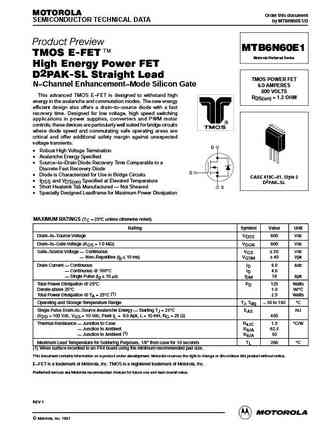
MOTOROLA Order this document SEMICONDUCTOR TECHNICAL DATA by MTP6N60E/D Designer's Data Sheet MTP6N60E TMOS E-FET. Motorola Preferred Device Power Field Effect Transistor N Channel Enhancement Mode Silicon Gate TMOS POWER FET This high voltage MOSFET uses an advanced termination 6.0 AMPERES scheme to provide enhanced voltage blocking capability without 600 VOLTS degra
mtb6n60erev2.pdf

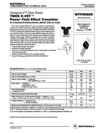
MOTOROLA Order this document SEMICONDUCTOR TECHNICAL DATA by MTB6N60E/D Designer's Data Sheet MTB6N60E TMOS E-FET. Motorola Preferred Device High Energy Power FET D2PAK for Surface Mount TMOS POWER FET N Channel Enhancement Mode Silicon Gate 6.0 AMPERES 600 VOLTS The D2PAK package has the capability of housing a larger die RDS(on) = 1.2 OHM than any existing surface mou
mtp6n60e.pdf
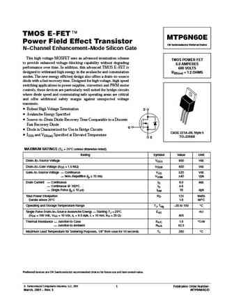
TMOS E-FET. MTP6N60E Power Field Effect Transistor ON Semiconductor Preferred Device N Channel Enhancement Mode Silicon Gate This high voltage MOSFET uses an advanced termination scheme TMOS POWER FET to provide enhanced voltage blocking capability without degrading 6.0 AMPERES performance over time. In addition, this advanced TMOS E FET is 600 VOLTS designed to withstand
mtb6n60e.pdf
MOTOROLA Order this document SEMICONDUCTOR TECHNICAL DATA by MTB6N60E/D Designer's Data Sheet MTB6N60E TMOS E-FET. Motorola Preferred Device High Energy Power FET D2PAK for Surface Mount TMOS POWER FET N Channel Enhancement Mode Silicon Gate 6.0 AMPERES 600 VOLTS The D2PAK package has the capability of housing a larger die RDS(on) = 1.2 OHM than any existing surface mou
irfb16n60l.pdf
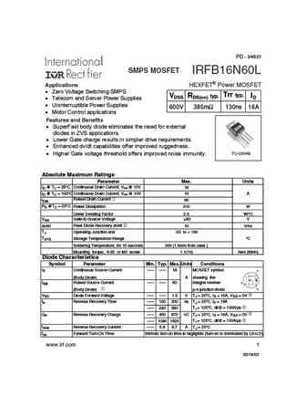
FOR REVIEW ONLY PD - TBD PD - 94631 SMPS MOSFET IRFB16N60L Applications HEXFET Power MOSFET Zero Voltage Switching SMPS Trr typ. VDSS RDS(on) typ. ID Telecom and Server Power Supplies Uninterruptible Power Supplies 600V 385m 130ns 16A Motor Control applications Features and Benefits SuperFast body diode eliminates the need for external diodes in ZVS appli
irfib6n60a.pdf
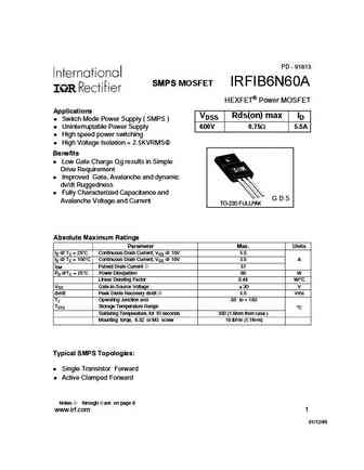
PD - 91813 SMPS MOSFET IRFIB6N60A HEXFET Power MOSFET Applications VDSS Rds(on) max ID l Switch Mode Power Supply ( SMPS ) l Uninterruptable Power Supply 600V 0.75W 5.5A l High speed power switching l High Voltage Isolation = 2.5KVRMS Benefits l Low Gate Charge Qg results in Simple Drive Requirement l Improved Gate, Avalanche and dynamic dv/dt Ruggedness l Fully Characterized
irfb16n60lpbf.pdf
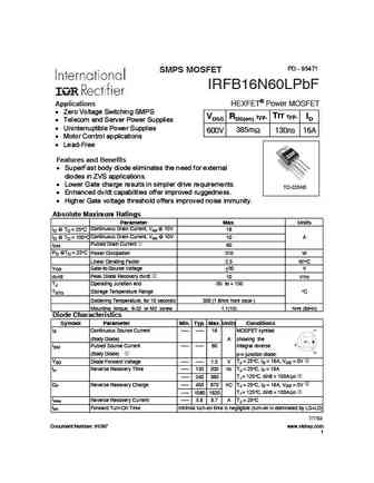
PD - 95471 SMPS MOSFET IRFB16N60LPbF Applications HEXFET Power MOSFET Zero Voltage Switching SMPS Trr typ. VDSS RDS(on) typ. ID Telecom and Server Power Supplies Uninterruptible Power Supplies 600V 385m 130ns 16A Motor Control applications Lead-Free Features and Benefits SuperFast body diode eliminates the need for external diodes in ZVS applications.
irfib6n60apbf.pdf
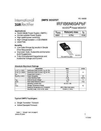
PD - 94838 SMPS MOSFET IRFIB6N60APbF HEXFET Power MOSFET Applications VDSS Rds(on) max ID l Switch Mode Power Supply ( SMPS ) l Uninterruptable Power Supply 600V 0.75 5.5A l High speed power switching l High Voltage Isolation = 2.5KVRMS l Lead-Free Benefits l Low Gate Charge Qg results in Simple Drive Requirement l Improved Gate, Avalanche and dynamic dv/dt Ruggedness G
phx6n60e.pdf
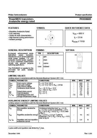
Philips Semiconductors Product specification PowerMOS transistors PHX6N60E Avalanche energy rated FEATURES SYMBOL QUICK REFERENCE DATA d Repetitive Avalanche Rated Fast switching VDSS = 600 V Stable off-state characteristics High thermal cycling performance ID = 2.8 A g Isolated package RDS(ON) 1.8 s GENERAL DESCRIPTION PINNING SOT186A N-channel, enh
php6n60e phb6n60e.pdf
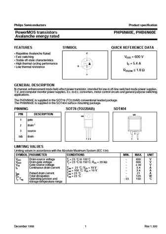
Philips Semiconductors Product specification PowerMOS transistors PHP6N60E, PHB6N60E Avalanche energy rated FEATURES SYMBOL QUICK REFERENCE DATA d Repetitive Avalanche Rated Fast switching VDSS = 600 V Stable off-state characteristics High thermal cycling performance ID = 5.4 A g Low thermal resistance RDS(ON) 1.8 s GENERAL DESCRIPTION N-channel, enh
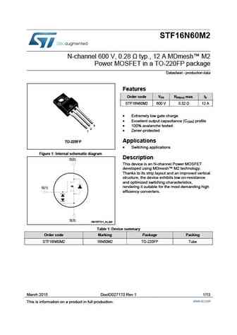
stp26n60m2 stw26n60m2.pdf
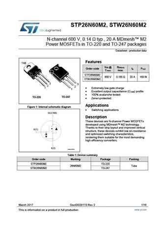
STP26N60M2, STW26N60M2 N-channel 600 V, 0.14 typ., 20 A MDmesh M2 Power MOSFETs in TO-220 and TO-247 packages Datasheet - production data Features TAB V @ R DS DS(on) Order code I P D TOT T max. Jmax STP26N60M2 650 V 0.165 20 A 169 W STW26N60M2 3 3 2 2 1 Extremely low gate charge 1 Excellent output capacitance (C ) profile OSS 100% avala
stl16n60m2.pdf
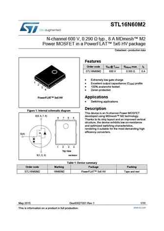
STL16N60M2 N-channel 600 V, 0.290 typ., 8 A MDmesh M2 Power MOSFET in a PowerFLAT 5x6 HV package Datasheet - production data Features Order code V @ T R max. I DS Jmax DS(on) D STL16N60M2 650 V 0.355 8 A Extremely low gate charge 1 Excellent output capacitance (COSS) profile 2 100% avalanche tested 3 4 Zener-protected Applications PowerFL
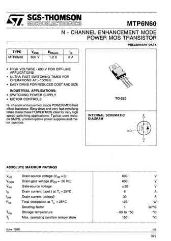
mtp6n60.pdf

MTP6N60 N - CHANNEL ENHANCEMENT MODE POWER MOS TRANSISTOR TYPE V R I DSS DS(on) D MTP6N60 600 V
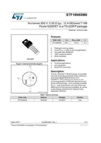
stf6n60m2 stp6n60m2 stu6n60m2.pdf
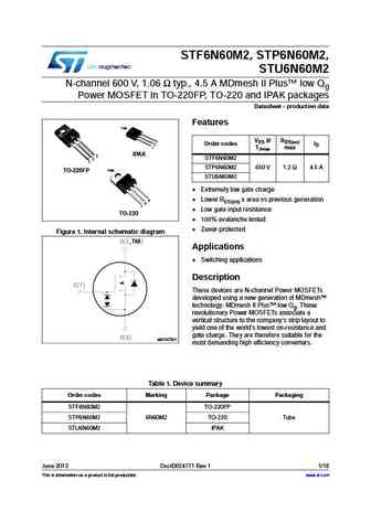
STF6N60M2, STP6N60M2, STU6N60M2 N-channel 600 V, 1.06 typ., 4.5 A MDmesh II Plus low Qg Power MOSFET in TO-220FP, TO-220 and IPAK packages Datasheet - production data Features TAB VDS @ RDS(on) 3 2 Order codes ID 1 TJmax max IPAK 3 STF6N60M2 2 1 STP6N60M2 650 V 1.2 4.5 A TO-220FP TAB STU6N60M2 Extremely low gate charge 3 Lower RDS(on) x area vs previous
stw56n60m2-4.pdf
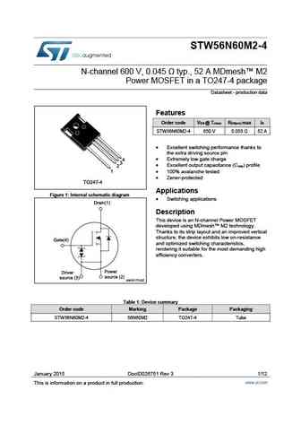
STW56N60M2-4 N-channel 600 V, 0.045 typ., 52 A MDmesh M2 Power MOSFET in a TO247-4 package Datasheet - production data Features Order code V Jmax DS(on) D DS @ T R max I STW56N60M2-4 650 V 0.055 52 A Excellent switching performance thanks to the extra driving source pin Extremely low gate charge Excellent output capacitance (C ) profile oss 100%
stw56n60m2.pdf
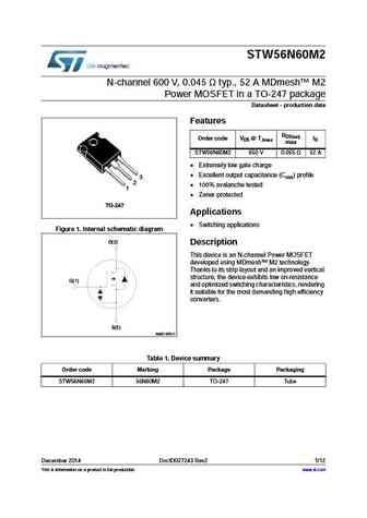
STW56N60M2 N-channel 600 V, 0.045 typ., 52 A MDmesh M2 Power MOSFET in a TO-247 package Datasheet - production data Features RDS(on) Order code VDS @ TJmax max ID STW56N60M2 650 V 0.055 52 A Extremely low gate charge Excellent output capacitance (Coss) profile 3 2 100% avalanche tested 1 Zener-protected TO-247 Applications Switching application
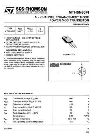
stp6n60fi.pdf

STP6N60FI N - CHANNEL ENHANCEMENT MODE POWER MOS TRANSISTOR TYPE VDSS RDS(on) ID STP6N60FI 600 V
std16n60m2.pdf
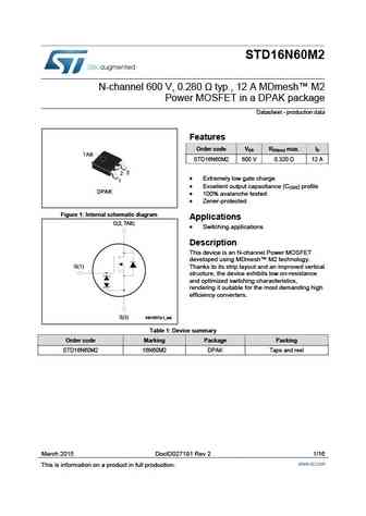
STD16N60M2 N-channel 600 V, 0.280 typ., 12 A MDmesh M2 Power MOSFET in a DPAK package Datasheet - production data Features Order code V R max. I DS DS(on) D STD16N60M2 600 V 0.320 12 A Extremely low gate charge Excellent output capacitance (COSS) profile 100% avalanche tested Zener-protected Figure 1 Internal schematic diagram Applications D(
stp16n60m2 stu16n60m2.pdf
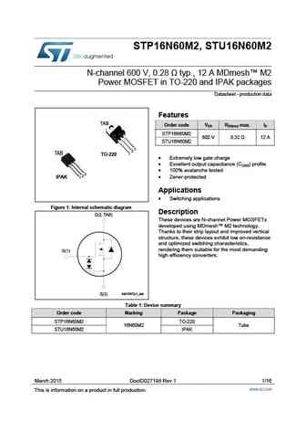
STP16N60M2, STU16N60M2 N-channel 600 V, 0.28 typ., 12 A MDmesh M2 Power MOSFET in TO-220 and IPAK packages Datasheet - production data Features TAB Order code V R max. I DS DS(on) D STP16N60M2 600 V 0.32 12 A STU16N60M2 3 2 TAB 1 TO-220 Extremely low gate charge Excellent output capacitance (COSS) profile 100% avalanche tested 3 2 IPAK
stb6n60m2 std6n60m2.pdf
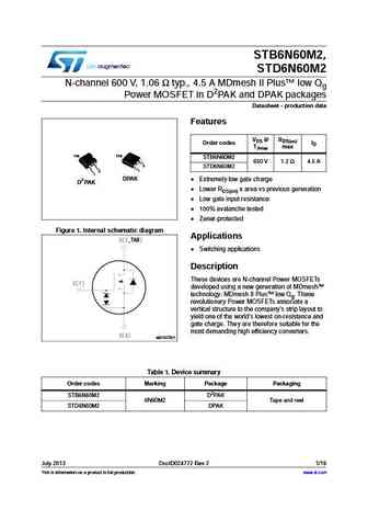
STB6N60M2, STD6N60M2 N-channel 600 V, 1.06 typ., 4.5 A MDmesh II Plus low Qg Power MOSFET in D2PAK and DPAK packages Datasheet - production data Features VDS @ RDS(on) Order codes ID TJmax max TAB TAB STB6N60M2 650 V 1.2 4.5 A 3 STD6N60M2 1 3 1 DPAK 2 Extremely low gate charge D PAK Lower RDS(on) x area vs previous generation Low gate input resistanc
stu6n60dm2.pdf
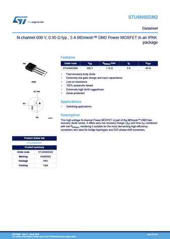
STU6N60DM2 Datasheet N-channel 600 V, 0.95 typ., 5 A MDmesh DM2 Power MOSFET in an IPAK package Features VDS RDS(on) max. ID PTOT TAB Order code STU6N60DM2 600 V 1.10 5 A 60 W 3 2 Fast-recovery body diode 1 Extremely low gate charge and input capacitance Low on-resistance IPAK 100% avalanche tested Extremely high dv/dt ruggedness D(2, TAB) Zen
stf16n60m2.pdf
STF16N60M2 N-channel 600 V, 0.28 typ., 12 A MDmesh M2 Power MOSFET in a TO-220FP package Datasheet - production data Features Order code V R max. I DS DS(on) D STF16N60M2 600 V 0.32 12 A Extremely low gate charge Excellent output capacitance (COSS) profile 3 100% avalanche tested 2 Zener-protected 1 Applications TO-220FP Switching applica
stp36n60m6 stw36n60m6.pdf
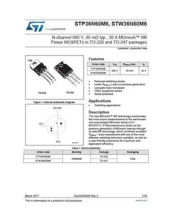
STP36N60M6, STW36N60M6 N-channel 600 V, 85 m typ., 30 A MDmesh M6 Power MOSFETs in TO-220 and TO-247 packages Datasheet - production data Features TAB Order code V R max. I DS DS(on) D STP36N60M6 600 V 99 m 30 A STW36N60M6 3 3 Reduced switching losses 2 2 1 Lower R x area vs previous generation DS(on) 1 Low gate input resistance 100% avalanche tested
stp6n60f.pdf
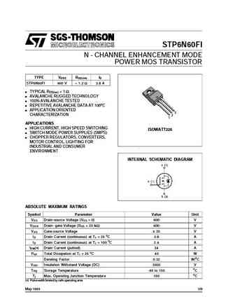
STP6N60FI N - CHANNEL ENHANCEMENT MODE POWER MOS TRANSISTOR TYPE V R I DSS DS(on) D STP6N60FI 600 V
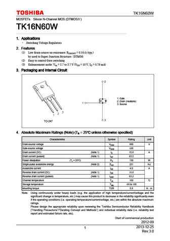
tk16n60w5.pdf

TK16N60W5 MOSFETs Silicon N-Channel MOS (DTMOS ) TK16N60W5 TK16N60W5 TK16N60W5 TK16N60W5 1. Applications 1. Applications 1. Applications 1. Applications Switching Voltage Regulators 2. Features 2. Features 2. Features 2. Features (1) Fast reverse recovery time trr = 100 ns (typ.) (2) Low drain-source on-resistance RDS(ON) = 0.18 (typ.) by used to Super Junction Str
tk16n60w.pdf
TK16N60W MOSFETs Silicon N-Channel MOS (DTMOS ) TK16N60W TK16N60W TK16N60W TK16N60W 1. Applications 1. Applications 1. Applications 1. Applications Switching Voltage Regulators 2. Features 2. Features 2. Features 2. Features (1) Low drain-source on-resistance RDS(ON) = 0.16 (typ.) by used to Super Junction Structure DTMOS (2) Easy to control Gate switching (3) En
fca16n60n.pdf
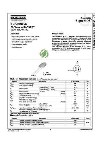
August 2009 SupreMOSTM FCA16N60N N-Channel MOSFET 600V, 16A, 0.170 Features Description RDS(on) = 0.17 ( Typ.)@ VGS = 10V, ID = 8A The SupreMOS MOSFET, Fairchild s next generation of high voltage super-junction MOSFETs, employs a deep trench filling Ultra low gate charge ( Typ. Qg = 40.2nC) process that differentiates it from preceding multi-epi based technologies. By
fca76n60n.pdf
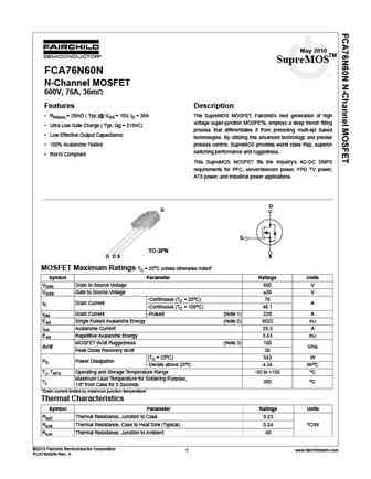
May 2010 SupreMOS TM FCA76N60N N-Channel MOSFET 600V, 76A, 36m Features Description RDS(on) = 28m ( Typ.)@ VGS = 10V, ID = 38A The SupreMOS MOSFET, Fairchild s next generation of high voltage super-junction MOSFETs, employs a deep trench filling Ultra Low Gate Charge ( Typ. Qg = 218nC) process that differentiates it from preceding multi-epi based Low Effective Ou
fqp6n60.pdf
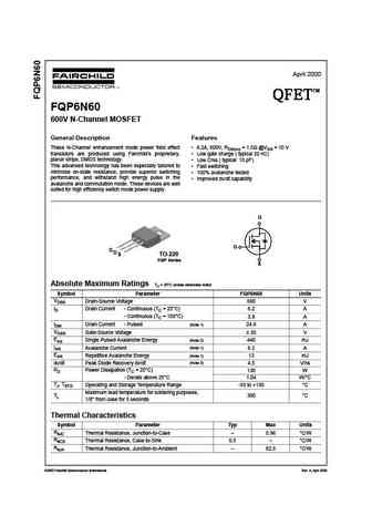
April 2000 TM QFET QFET QFET QFET FQP6N60 600V N-Channel MOSFET General Description Features These N-Channel enhancement mode power field effect 6.2A, 600V, RDS(on) = 1.5 @VGS = 10 V transistors are produced using Fairchild s proprietary, Low gate charge ( typical 20 nC) planar stripe, DMOS technology. Low Crss ( typical 10 pF) This advanced technology has been esp
sgr6n60uf.pdf
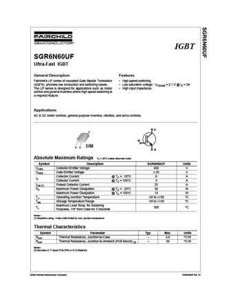
IGBT SGR6N60UF Ultra-Fast IGBT General Description Features Fairchild's UF series of Insulated Gate Bipolar Transistors High speed switching (IGBTs) provides low conduction and switching losses. Low saturation voltage VCE(sat) = 2.1 V @ IC = 3A The UF series is designed for applications such as motor High input impedance control and general inverters where high speed swit
fch76n60n.pdf
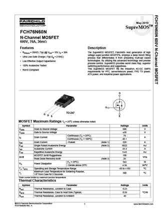
May 2010 SupreMOSTM FCH76N60N N-Channel MOSFET 600V, 76A, 36m Features Description RDS(on) = 28m ( Typ.)@ VGS = 10V, ID = 38A The SupreMOS MOSFET, Fairchild s next generation of high voltage super-junction MOSFETs, employs a deep trench filling Ultra Low Gate Charge ( Typ.Qg = 218nC) process that differentiates it from preceding multi-epi based technologies. By utili
fqb6n60ctm fqi6n60ctu.pdf
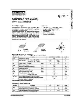
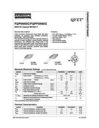
QFET FQB6N60C / FQI6N60C 600V N-Channel MOSFET General Description Features These N-Channel enhancement mode power field effect 5.5A, 600V, RDS(on) = 2.0 @VGS = 10 V transistors are produced using Fairchild s proprietary, Low gate charge ( typical 16 nC) planar stripe, DMOS technology. Low Crss ( typical 7 pF) This advanced technology has been especially tailored to
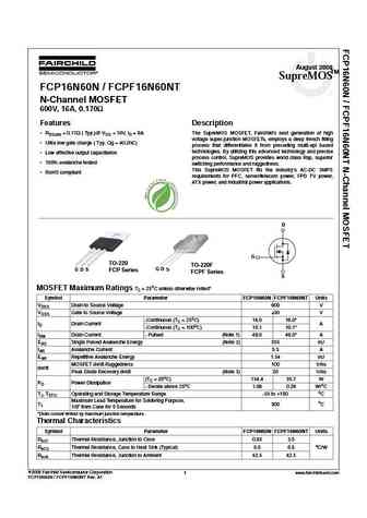
fcp16n60 fcpf16n60.pdf
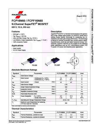
August 2014 FCP16N60 / FCPF16N60 N-Channel SuperFET MOSFET 600 V, 16 A, 260 m Features Description SuperFET MOSFET is Fairchild Semiconductor s first genera- 650V @ TJ = 150 C tion of high voltage super-junction (SJ) MOSFET family that is Typ. RDS(on) = 220 m utilizing charge balance technology for outstanding low on- Ultra Low Gate Charge (Typ. Qg = 55 nC ) r
fca16n60 fca16n60 f109.pdf
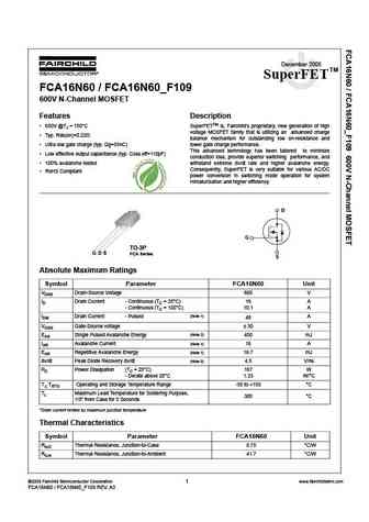
December 2008 TM SuperFET FCA16N60 / FCA16N60_F109 600V N-Channel MOSFET Features Description 650V @TJ = 150 C SuperFETTM is, Fairchild s proprietary, new generation of high voltage MOSFET family that is utilizing an advanced charge Typ. Rds(on)=0.22 balance mechanism for outstanding low on-resistance and Ultra low gate charge (typ. Qg=55nC) lower gate charge perfor
fqd6n60ctm.pdf
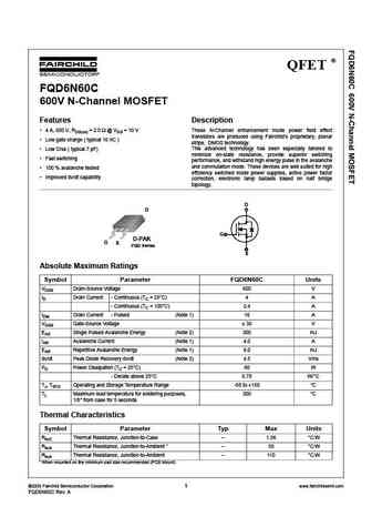
QFET FQD6N60C 600V N-Channel MOSFET Features Description 4 A, 600 V, RDS(on) = 2.0 @ VGS = 10 V These N-Channel enhancement mode power field effect transistors are produced using Fairchild s proprietary, planar Low gate charge ( typical 16 nC ) stripe, DMOS technology. This advanced technology has been especially tailored to Low Crss ( typical 7 pF) minimize on-s
fqb6n60tm.pdf
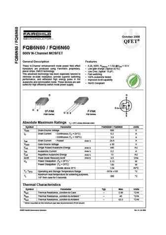
October 2008 QFET FQB6N60 / FQI6N60 600V N-Channel MOSFET General Description Features These N-Channel enhancement mode power field effect 6.2A, 600V, RDS(on) = 1.5 @VGS = 10 V transistors are produced using Fairchild s proprietary, Low gate charge ( typical 20 nC) planar stripe, DMOS technology. Low Crss ( typical 10 pF) This advanced technology has been especially
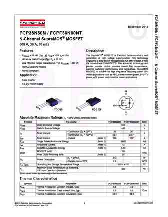
fcb36n60n fcb36n60ntm.pdf
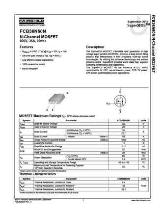
September 2010 SupreMOSTM FCB36N60N N-Channel MOSFET 600V, 36A, 90m Features Description RDS(on) = 81m ( Typ.)@ VGS = 10V, ID = 18A The SupreMOS MOSFET, Fairchild s next generation of high voltage super-junction MOSFETs, employs a deep trench filling Ultra low gate charge ( Typ. Qg = 86nC) process that differentiates it from preceding multi-epi based technologies.
fqpf6n60.pdf
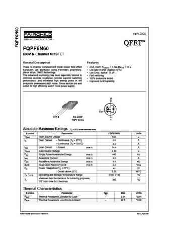
April 2000 TM QFET QFET QFET QFET FQPF6N60 600V N-Channel MOSFET General Description Features These N-Channel enhancement mode power field effect 3.6A, 600V, RDS(on) = 1.5 @VGS = 10 V transistors are produced using Fairchild s proprietary, Low gate charge ( typical 20 nC) planar stripe, DMOS technology. Low Crss ( typical 10 pF) This advanced technology has been es
fqp6n60c fqp6n60c fqpf6n60c fqpf6n60c.pdf
QFET FQP6N60C/FQPF6N60C 600V N-Channel MOSFET General Description Features These N-Channel enhancement mode power field effect 5.5A, 600V, RDS(on) = 2.0 @VGS = 10 V transistors are produced using Fairchild s proprietary, Low gate charge ( typical 16 nC) planar stripe, DMOS technology. Low Crss ( typical 7 pF) This advanced technology has been especially tailored to
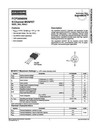
fcp16n60n fcpf16n60nt.pdf
August 2009 SupreMOSTM FCP16N60N / FCPF16N60NT N-Channel MOSFET 600V, 16A, 0.170 Features Description RDS(on) = 0.17 ( Typ.)@ VGS = 10V, ID = 8A The SupreMOS MOSFET, Fairchild s next generation of high voltage super-junction MOSFETs, employs a deep trench filling Ultra low gate charge ( Typ. Qg = 40.2nC) process that differentiates it from preceding multi-epi based te
fdp6n60zu fdpf6n60zut.pdf
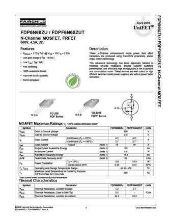
April 2009 UniFETTM FDP6N60ZU / FDPF6N60ZUT N-Channel MOSFET, FRFET 600V, 4.5A, 2 Features Description RDS(on) = 1.7 ( Typ.) @ VGS = 10V, ID = 2.25A These N-Channel enhancement mode power field effect transistors are produced using Fairchild s proprietary, planar Low gate charge ( Typ. 14.5nC) stripe, DMOS technology. Low Crss ( Typ. 5pF) This advanced technology
fcp16n60 fcpf16n60.pdf
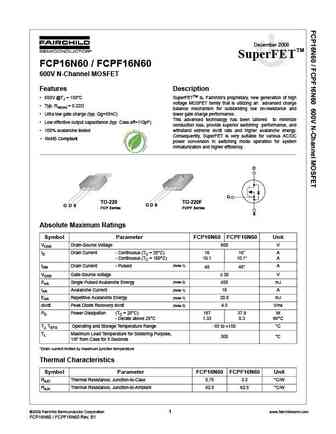
December 2008 TM SuperFET FCP16N60 / FCPF16N60 600V N-Channel MOSFET Features Description 650V @TJ = 150 C SuperFETTM is, Fairchild s proprietary, new generation of high voltage MOSFET family that is utilizing an advanced charge Typ. Rds(on) = 0.22 balance mechanism for outstanding low on-resistance and Ultra low gate charge (typ. Qg=55nC) lower gate charge perfo
fca36n60nf.pdf
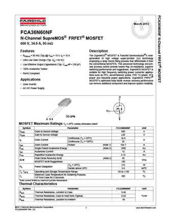
March 2013 FCA36N60NF N-Channel SupreMOS FRFET MOSFET 600 V, 34.9 A, 95 m Features Description RDS(on) = 80 m (Typ.)@ VGS = 10 V, ID = 18 A The SupreMOS MOSFET is Fairchild Semiconductor s next- generation of high voltage super-junction (SJ) technology Ultra Low Gate Charge (Typ. Qg = 86 nC) employing a deep trench filling process that differentiate it from th
fqd6n60c.pdf

QFET FQD6N60C 600V N-Channel MOSFET Features Description 4 A, 600 V, RDS(on) = 2.0 @ VGS = 10 V These N-Channel enhancement mode power field effect transistors are produced using Fairchild s proprietary, planar Low gate charge ( typical 16 nC ) stripe, DMOS technology. This advanced technology has been especially tailored to Low Crss ( typical 7 pF) minimize on-s
fcp36n60n.pdf
November 2010 SupreMOSTM FCP36N60N tm N-Channel MOSFET 600V, 36A, 90m Features Description RDS(on) = 81m ( Typ.)@ VGS = 10V, ID = 18A The SupreMOS MOSFET, Fairchild s next generation of high voltage super-junction MOSFETs, employs a deep trench filling Ultra low gate charge ( Typ. Qg = 86nC) process that differentiates it from preceding multi-epi based technologies.
fch76n60nf.pdf

January 2011 SupreMOS FCH76N60NF tm 600V N-Channel MOSFET, FRFET Features Description RDS(on) = 28.7m ( Typ.)@ VGS = 10V, ID = 38A The SupreMOS MOSFET, Fairchild s next generation of high voltage super-junction MOSFETs, employs a deep trench filling Ultra Low Gate Charge ( Typ.Qg = 230nC) process that differentiates it from preceding multi-epi based technologies. By
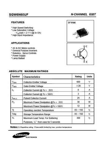
sgw6n60ufd.pdf
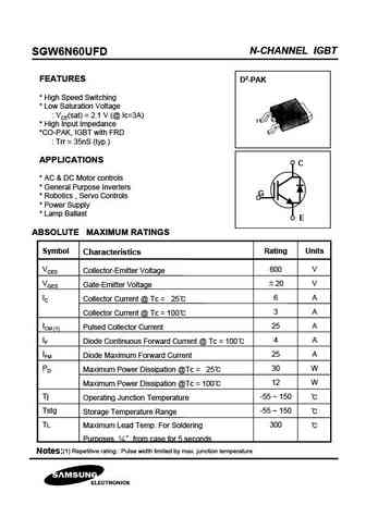
N-CHANNEL IGBT SGW6N60UFD FEATURES D2-PAK * High Speed Switching * Low Saturation Voltage VCE(sat) = 2.1 V (@ Ic=3A) * High Input Impedance *CO-PAK, IGBT with FRD Trr = 35nS (typ.) APPLICATIONS C * AC & DC Motor controls * General Purpose Inverters G * Robotics , Servo Controls * Power Supply * Lamp Ballast E ABSOLUTE MAXIMUM RATINGS Symbol Rating Units Characteri
sgw6n60uf.pdf
N-CHANNEL IGBT SGW6N60UF FEATURES D2-PAK * High Speed Switching * Low Saturation Voltage VCE(sat) = 2.1 V (@ Ic=3A) * High Input Impedance APPLICATIONS C * AC & DC Motor controls * General Purpose Inverters * Robotics , Servo Controls G * Power Supply * Lamp Ballast E ABSOLUTE MAXIMUM RATINGS Symbol Rating Units Characteristics VCES 600 V Collector-Emitter Voltage VG
sgp6n60ufd.pdf
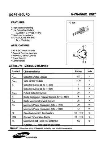
N-CHANNEL IGBT SGP6N60UFD FEATURES TO-220 * High Speed Switching * Low Saturation Voltage VCE(sat) = 2.1 V (@ Ic=3A) * High Input Impedance *CO-PAK, IGBT with FRD Trr = 35nS (typ.) APPLICATIONS C * AC & DC Motor controls * General Purpose Inverters G * Robotics , Servo Controls * Power Supply * Lamp Ballast E ABSOLUTE MAXIMUM RATINGS Symbol Rating Units Characteri
sgp6n60uf.pdf
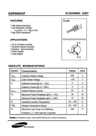
N-CHANNEL IGBT SGP6N60UF FEATURES TO-220 * High Speed Switching * Low Saturation Voltage VCE(sat) = 2.1 V (@ Ic=3A) * High Input Impedance APPLICATIONS C * AC & DC Motor controls * General Purpose Inverters * Robotics , Servo Controls G * Power Supply * Lamp Ballast E ABSOLUTE MAXIMUM RATINGS Symbol Rating Units Characteristics VCES 600 V Collector-Emitter Voltage VG
sgu6n60uf.pdf
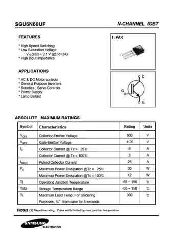
N-CHANNEL IGBT SGU6N60UF FEATURES I - PAK * High Speed Switching * Low Saturation Voltage VCE(sat) = 2.1 V (@ Ic=3A) * High Input Impedance APPLICATIONS C * AC & DC Motor controls * General Purpose Inverters * Robotics , Servo Controls G * Power Supply * Lamp Ballast E ABSOLUTE MAXIMUM RATINGS Symbol Rating Units Characteristics VCES 600 V Collector-Emitter Voltage V
irfp26n60l irfp26n60lpbf sihfp26n60l.pdf

IRFP26N60L, SiHFP26N60L Vishay Siliconix Power MOSFET FEATURES PRODUCT SUMMARY Superfast Body Diode Eliminates the Need for VDS (V) 600 Available External Diodes in ZVS Applications RDS(on) ( )VGS = 10 V 0.21 RoHS* Lower Gate Charge Results in Simpler Drive Qg (Max.) (nC) 180 COMPLIANT Requirements Qgs (nC) 61 Enhanced dV/dt Capabilities Offer Improved Ruggedness
irfib6n60a sihfib6n60a.pdf
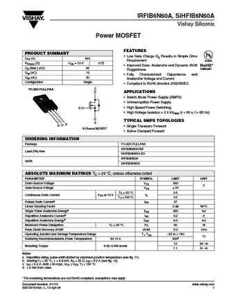
IRFIB6N60A, SiHFIB6N60A Vishay Siliconix Power MOSFET FEATURES PRODUCT SUMMARY Low Gate Charge Qg Results in Simple Drive VDS (V) 600 Requirement Available RDS(on) ( )VGS = 10 V 0.75 Improved Gate, Avalanche and Dynamic dV/dt RoHS* Qg (Max.) (nC) 49 COMPLIANT Ruggedness Qgs (nC) 13 Fully Characterized Capacitance and Qgd (nC) 20 Avalanche Voltage and Current Confi
irfb16n60lpbf.pdf
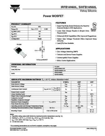
IRFB16N60L, SiHFB16N60L Vishay Siliconix Power MOSFET FEATURES PRODUCT SUMMARY Super Fast Body Diode Eliminates the Need for VDS (V) 600 Available External Diodes in ZVS Applications RDS(on) ( )VGS = 10 V 0.385 RoHS* COMPLIANT Lower Gate Charge Results in Simpler Drive Qg (Max.) (nC) 100 Requirements Qgs (nC) 30 Enhanced dV/dt Capabilities Offer Improved Ruggedness
sihfib6n60a.pdf

IRFIB6N60A, SiHFIB6N60A Vishay Siliconix Power MOSFET FEATURES PRODUCT SUMMARY Low Gate Charge Qg Results in Simple Drive VDS (V) 600 Requirement Available RDS(on) ( )VGS = 10 V 0.75 Improved Gate, Avalanche and Dynamic dV/dt RoHS* Qg (Max.) (nC) 49 COMPLIANT Ruggedness Qgs (nC) 13 Fully Characterized Capacitance and Qgd (nC) 20 Avalanche Voltage and Current Confi
irfp26n60l sihfp26n60l.pdf
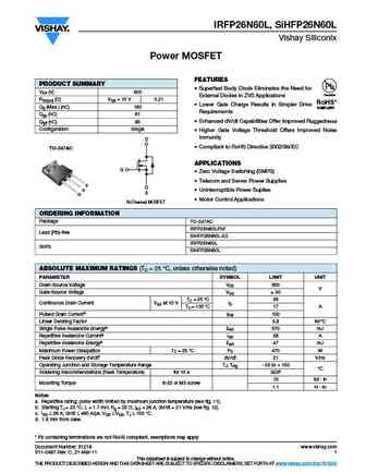
IRFP26N60L, SiHFP26N60L Vishay Siliconix Power MOSFET FEATURES PRODUCT SUMMARY Superfast Body Diode Eliminates the Need for VDS (V) 600 Available External Diodes in ZVS Applications RDS(on) ( )VGS = 10 V 0.21 RoHS* Lower Gate Charge Results in Simpler Drive Qg (Max.) (nC) 180 COMPLIANT Requirements Qgs (nC) 61 Enhanced dV/dt Capabilities Offer Improved Ruggedness
sihh26n60e.pdf

SiHH26N60E www.vishay.com Vishay Siliconix E Series Power MOSFET FEATURES PRODUCT SUMMARY Fully lead (Pb)-free device VDS (V) at TJ max. 650 Low figure-of-merit (FOM) Ron x Qg RDS(on) typ. ( ) at 25 C VGS = 10 V 0.117 Low input capacitance (Ciss) Qg max. (nC) 116 Reduced switching and conduction losses Qgs (nC) 18 Qgd (nC) 33 Ultra low gate charge (Qg) Con
sgb06n60.pdf

SGB06N60 Fast IGBT in NPT-technology 75% lower Eoff compared to previous generation combined with low conduction losses C Short circuit withstand time 10 s Designed for - Motor controls G E - Inverter NPT-Technology for 600V applications offers - very tight parameter distribution - high ruggedness, temperature stable behaviour PG-TO-263-3-2 (D -P
sgb06n60 .pdf
SGB06N60 Fast IGBT in NPT-technology 75% lower Eoff compared to previous generation combined with low conduction losses C Short circuit withstand time 10 s Designed for - Motor controls G E - Inverter NPT-Technology for 600V applications offers - very tight parameter distribution - high ruggedness, temperature stable behaviour PG-TO-263-3-2 (D -P
skp06n60 ska06n60.pdf

SKP06N60 SKA06N60 Fast IGBT in NPT-technology with soft, fast recovery anti-parallel EmCon diode C 75% lower Eoff compared to previous generation combined with low conduction losses Short circuit withstand time 10 s G E Designed for Motor controls, Inverter NPT-Technology for 600V applications offers - very tight parameter distribution - high ruggedn
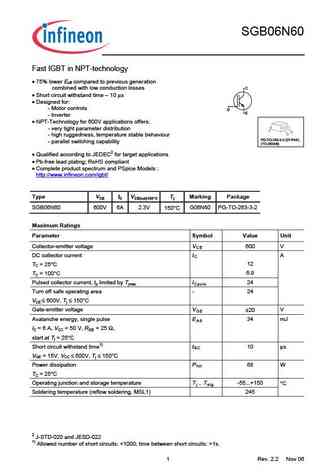
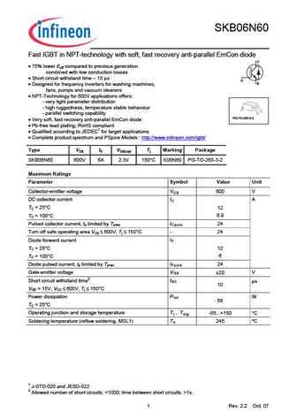
skb06n60.pdf

SKB06N60 Fast IGBT in NPT-technology with soft, fast recovery anti-parallel EmCon diode C 75% lower Eoff compared to previous generation combined with low conduction losses Short circuit withstand time 10 s G E Designed for frequency inverters for washing machines, fans, pumps and vacuum cleaners NPT-Technology for 600V applications offers - very tight
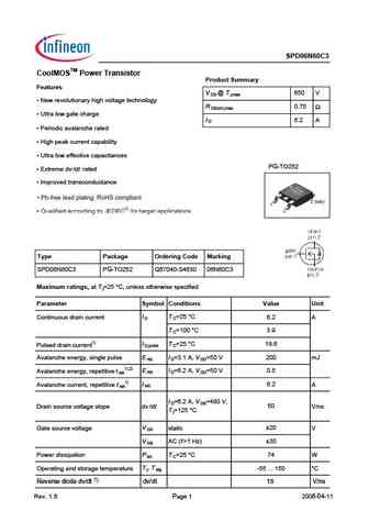
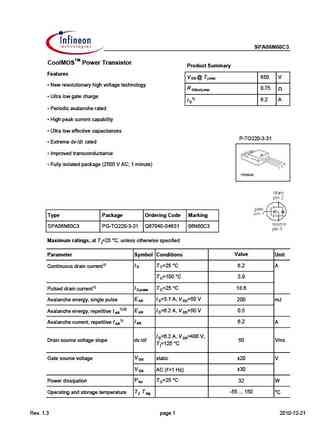
spp06n60c3.pdf
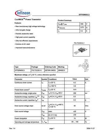
SPP06N60C3 CoolMOSTM Power Transistor Product Summary Features V @ T 650 V DS j,max New revolutionary high voltage technology R 0.75 DS(on),max Ultra low gate charge I 6.2 A D Periodic avalanche rated High peak current capability Ultra low effective capacitances PG-TO220-3-1 Extreme dv /dt rated Improved transconductance Type Package Ordering Co
skb06n60g.pdf
SKB06N60 Fast IGBT in NPT-technology with soft, fast recovery anti-parallel EmCon diode C 75% lower Eoff compared to previous generation combined with low conduction losses Short circuit withstand time 10 s G E Designed for frequency inverters for washing machines, fans, pumps and vacuum cleaners NPT-Technology for 600V applications offers - very tight
ihd06n60ra.pdf
IHD06N60RA Soft Switching Series Reverse conducting IGBT with monolithic body diode C Powerful monolithic body diode with low forward voltage designed for soft commutation only TrenchStop technology applications offers G E - very tight parameter distribution - high ruggedness, temperature stable behavior - low V CEsat - easy parallel switching capability due to pos
skb06n60hs.pdf
SKB06N60HS High Speed IGBT in NPT-technology C 30% lower Eoff compared to previous generation Short circuit withstand time 10 s G E Designed for operation above 30 kHz NPT-Technology for 600V applications offers PG-TO-263-3-2 - parallel switching capability - moderate Eoff increase with temperature - very tight parameter distribution High ruggedn
sgp06n60.pdf

SGP06N60 SGD06N60 Fast IGBT in NPT-technology 75% lower Eoff compared to previous generation combined with low conduction losses C Short circuit withstand time 10 s Designed for - Motor controls G E - Inverter NPT-Technology for 600V applications offers - very tight parameter distribution - high ruggedness, temperature stable behaviour PG-TO-252
ihd06n60ra 1 3.pdf

IHD06N60RA Soft Switching Series Reverse conducting IGBT with monolithic body diode C Powerful monolithic body diode with low forward voltage designed for soft commutation only TrenchStop technology applications offers G E - very tight parameter distribution - high ruggedness, temperature stable behavior - low V CEsat - easy parallel switching capability due to pos
ika06n60trev2 3g.pdf
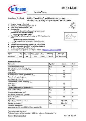
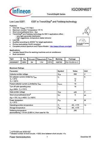
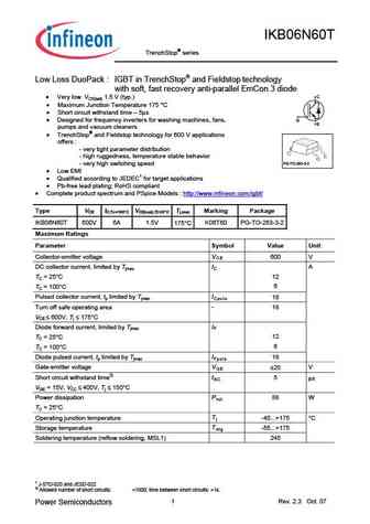
IKA06N60T TrenchStop Series Low Loss DuoPack IGBT in TrenchStop and Fieldstop technology with soft, fast recovery anti-parallel EmCon HE diode Features C Very low VCE(sat) 1.5 V (typ.) Maximum Junction Temperature 175 C Short circuit withstand time 5 s G E TrenchStop and Fieldstop technology for 600 V applications offers - very tigh
sgd06n60.pdf

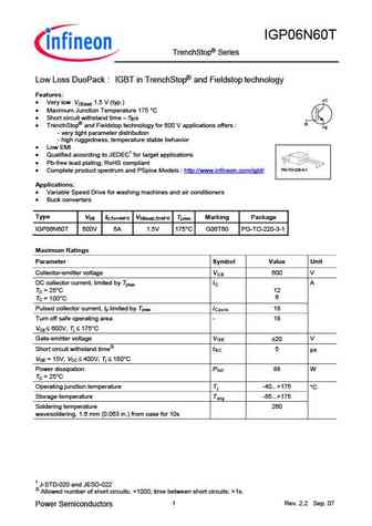
SGP06N60 SGD06N60 Fast IGBT in NPT-technology 75% lower Eoff compared to previous generation combined with low conduction losses C Short circuit withstand time 10 s Designed for - Motor controls G E - Inverter NPT-Technology for 600V applications offers - very tight parameter distribution - high ruggedness, temperature stable behaviour PG-TO-252
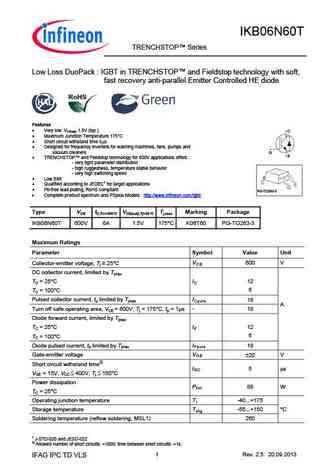
ika06n60t.pdf
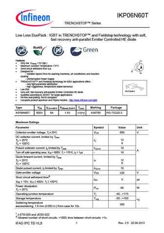
IKA06N60T TRENCHSTOP Series Low Loss DuoPack IGBT in TRENCHSTOP and Fieldstop technology with soft, fast recovery anti-parallel Emitter Controlled HE diode Features C Very low VCE(sat) 1.5V (typ.) Maximum Junction Temperature 175 C Short circuit withstand time 5 s TRENCHSTOP and Fieldstop technology for 600V applications offers G E - very
ikp06n60trev2 3g.pdf
IKP06N60T TrenchStop Series p Low Loss DuoPack IGBT in TrenchStop and Fieldstop technology with soft, fast recovery anti-parallel EmCon HE diode C Very low VCE(sat) 1.5 V (typ.) Maximum Junction Temperature 175 C Short circuit withstand time 5 s G E Designed for - Variable Speed Drive for washing machines, air conditioners and induction cooki
ikd06n60-rf.pdf
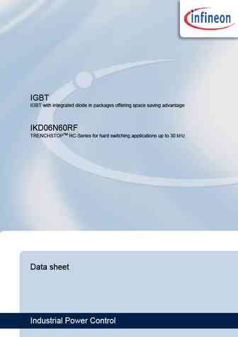
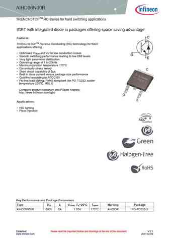
IGBT IGBT with integrated diode in packages offering space saving advantage IKD06N60RF TRENCHSTOPTM RC-Series for hard switching applications up to 30 kHz Data sheet Industrial Power Control IKD06N60RF TRENCHSTOPTM RC-Drives Fast Series IGBT with integrated diode in packages offering space saving advantage C Features TRENCHSTOPTM Reverse Conducting (RC) technology for 600V applica
sgp06n60 sgd06n60g.pdf
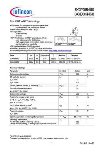
SGP06N60 SGD06N60 Fast IGBT in NPT-technology 75% lower Eoff compared to previous generation combined with low conduction losses C Short circuit withstand time 10 s Designed for - Motor controls G E - Inverter NPT-Technology for 600V applications offers - very tight parameter distribution - high ruggedness, temperature stable behaviour PG-TO-252
ska06n60.pdf

SKP06N60 SKA06N60 Fast IGBT in NPT-technology with soft, fast recovery anti-parallel EmCon diode C 75% lower Eoff compared to previous generation combined with low conduction losses Short circuit withstand time 10 s G E Designed for Motor controls, Inverter NPT-Technology for 600V applications offers - very tight parameter distribution - high ruggedn
igd06n60trev2 1.pdf
IGD06N60T TrenchStop Series q Low Loss IGBT IGBT in TrenchStop and Fieldstop technology Features C Very low VCE(sat) 1.5 V (typ.) Maximum Junction Temperature 175 C Short circuit withstand time 5 s G TrenchStop and Fieldstop technology for 600 V applications offers E - very tight parameter distribution - high ruggedness, temperature stabl
spd06n60c3.pdf
SPD06N60C3 CoolMOSTM Power Transistor Product Summary Features V @ T 650 V DS j,max New revolutionary high voltage technology R 0.75 DS(on),max Ultra low gate charge I 6.2 A D Periodic avalanche rated High peak current capability Ultra low effective capacitances PG-TO252 Extreme dv /dt rated Improved transconductance Type Package Ordering Code
ikd06n60ra.pdf
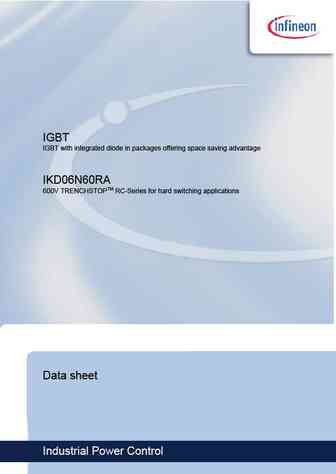
IGBT IGBT with integrated diode in packages offering space saving advantage IKD06N60RA 600V TRENCHSTOPTM RC-Series for hard switching applications Data sheet Industrial Power Control IKD06N60RA TRENCHSTOPTM RC-Series for hard switching applications IGBT with integrated diode in packages offering space saving advantage C Features TRENCHSTOPTM Reverse Conducting (RC) technology for 6
igd06n60t.pdf
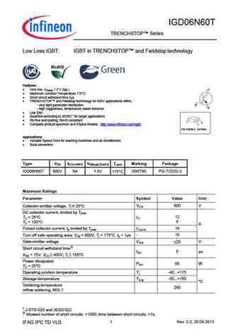
IGD06N60T TRENCHSTOP Series q Low Loss IGBT IGBT in TRENCHSTOP and Fieldstop technology Features Very low VCE(sat) 1.5 V (typ.) C Maximum Junction Temperature 175 C Short circuit withstand time 5 s TRENCHSTOP and Fieldstop technology for 600V applications offers - very tight parameter distribution G E - high ruggedness, temperature stable beha
skp06n60.pdf
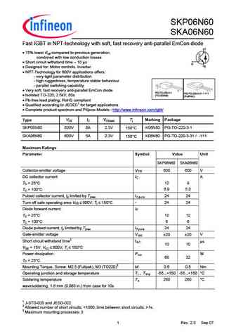
SKP06N60 SKA06N60 Fast IGBT in NPT-technology with soft, fast recovery anti-parallel EmCon diode C 75% lower Eoff compared to previous generation combined with low conduction losses Short circuit withstand time 10 s G E Designed for Motor controls, Inverter NPT-Technology for 600V applications offers - very tight parameter distribution - high ruggedn
iku06n60r.pdf
IGBT IGBT with integrated diode in packages offering space saving advantage IKD06N60R, IKU06N60R 600V TRENCHSTOPTM RC-Series for hard switching applications Datasheet Industrial & Multimarket IKD06N60R, IKU06N60R TRENCHSTOPTM RC-Series for hard switching applications IGBT with integrated diode in packages offering space saving advantage C Features TRENCHSTOPTM Reverse Conducting (R
spa06n60c3.pdf
SPA06N60C3 CoolMOSTM Power Transistor Product Summary Features V @ T 650 V DS j,max New revolutionary high voltage technology R 0.75 DS(on),max Ultra low gate charge 1) 6.2 A I D Periodic avalanche rated High peak current capability Ultra low effective capacitances P-TO220-3-31 Extreme dv /dt rated Improved transconductance Fully isolated
ikp06n60t.pdf
IKP06N60T TRENCHSTOP Series p Low Loss DuoPack IGBT in TRENCHSTOP and Fieldstop technology with soft, fast recovery anti-parallel Emitter Controlled HE diode Features C Very low VCE(sat) 1.5V (typ.) Maximum Junction Temperature 175 C Short circuit withstand time 5 s Designed for G E - Variable Speed Drive for washing machines, air conditioners and inducti
ikd06n60r.pdf

IGBT IGBT with integrated diode in packages offering space saving advantage IKD06N60R 600V TRENCHSTOPTM RC-Series for hard switching applications Data sheet Industrial Power Control IKD06N60R TRENCHSTOPTM RC-Series for hard switching applications IGBT with integrated diode in packages offering space saving advantage C Features TRENCHSTOPTM Reverse Conducting (RC) technology for 600
igp06n60t.pdf
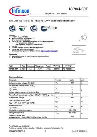
IGP06N60T TRENCHSTOP Series q Low Loss IGBT IGBT in TRENCHSTOP and Fieldstop technology C Features Very low VCE(sat) 1.5V (typ.) Maximum Junction Temperature 175 C Short circuit withstand time 5 s G E TRENCHSTOP and Fieldstop technology for 600V applications offers - very tight parameter distribution - high ruggedness, temperature stable behavior
ikd06n60rf.pdf

IGBT IGBT with integrated diode in packages offering space saving advantage IKD06N60RF TRENCHSTOPTM RC-Series for hard switching applications up to 30 kHz Data sheet Industrial Power Control IKD06N60RF TRENCHSTOPTM RC-Drives Fast Series IGBT with integrated diode in packages offering space saving advantage C Features TRENCHSTOPTM Reverse Conducting (RC) technology for 600V applica
skb06n60hsg.pdf

SKB06N60HS High Speed IGBT in NPT-technology C 30% lower Eoff compared to previous generation Short circuit withstand time 10 s G E Designed for operation above 30 kHz NPT-Technology for 600V applications offers PG-TO-263-3-2 - parallel switching capability - moderate Eoff increase with temperature - very tight parameter distribution High ruggedn
ikb06n60trev2 3g.pdf
IKB06N60T TrenchStop series p Low Loss DuoPack IGBT in TrenchStop and Fieldstop technology with soft, fast recovery anti-parallel EmCon 3 diode C Very low VCE(sat) 1.5 V (typ.) Maximum Junction Temperature 175 C Short circuit withstand time 5 s Designed for frequency inverters for washing machines, fans, G E pumps and vacuum cleaners TrenchSto
aihd06n60r.pdf
AIHD06N60R TRENCHSTOPTM RC-Series for hard switching applications IGBT with integrated diode in packages offering space saving advantage C Features TRENCHSTOPTM Reverse Conducting (RC) technology for 600V applications offering Optimised V and V for low conduction losses CEsat F G Smooth switching performance leading to low EMI levels E Very tight parameter distribution
igp06n60trev2 2g.pdf
IGP06N60T TrenchStop Series q Low Loss DuoPack IGBT in TrenchStop and Fieldstop technology Features C Very low VCE(sat) 1.5 V (typ.) Maximum Junction Temperature 175 C Short circuit withstand time 5 s G TrenchStop and Fieldstop technology for 600 V applications offers E - very tight parameter distribution - high ruggedness, temper
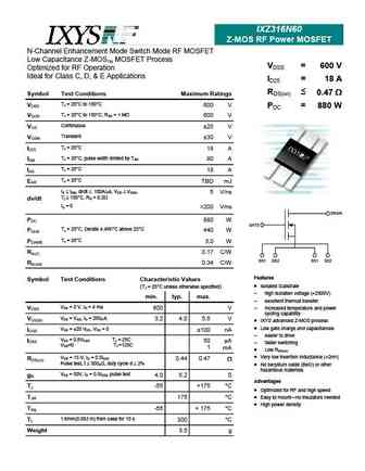
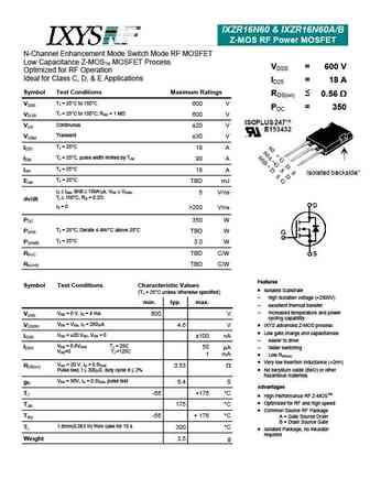
ixz316n60.pdf
IXZ316N60 Z-MOS RF Power MOSFET N-Channel Enhancement Mode Switch Mode RF MOSFET Low Capacitance Z-MOSTM MOSFET Process VDSS = 600 V Optimized for RF Operation Ideal for Class C, D, & E Applications ID25 = 18 A RDS(on) Symbol Test Conditions Maximum Ratings 0.47 TJ = 25 C to 150 C VDSS 600 V PDC = 880 W TJ = 25 C to 150 C; RGS = 1 M VDGR
ixzr16n60a ixzr16n60b.pdf
IXZR16N60 & IXZR16N60A/B Z-MOS RF Power MOSFET NChannel Enhancement Mode N-Channel Enhancement Mode Switch Mode RF MOSFET Low Qg and Rg Low Capacitance Z-MOSTM MOSFET Process VDSS = 600 V High dv/dt Optimized for RF Operation Nanosecond Switching Ideal for Class C, D, & E Applications ID25 = 18 A Symbol Test Conditions Maximum Ratings RDS(on) 0.56
ixsa16n60 ixsp16n60.pdf
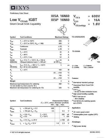
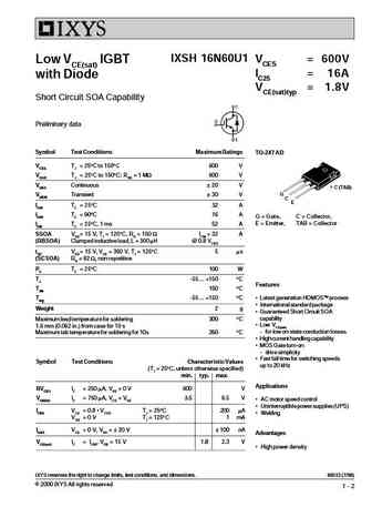
Preliminary Data Sheet IXSA 16N60 VCES = 600V Low VCE(sat) IGBT IXSP 16N60 IC25 = 16A Short Circuit SOA Capability VCE(sat)typ = 1.8V TO-220AB(IXSP) Symbol Test Conditions Maximum Ratings VCES TJ = 25 C to 150 C 600 V VCGR TJ = 25 C to 150 C; RGE = 1 M 600 V G C E VGES Continuous 20 V VGEM Transient 30 V TO-263AA IC25 TC = 25 C32 A IC90 TC = 90 C16 A ICM TC = 25
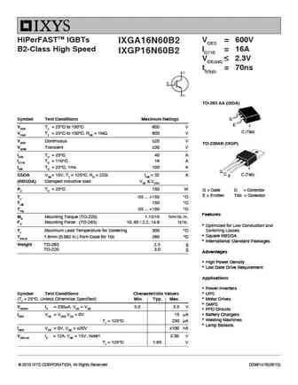
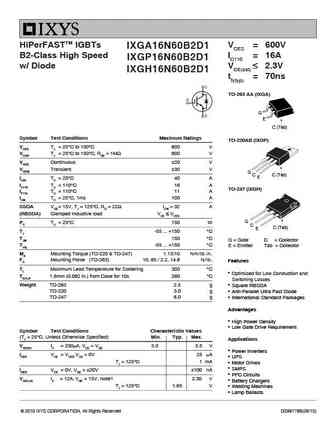
ixga16n60b2d1.pdf

HiPerFASTTM IGBTs VCES = 600V IXGA16N60B2D1 B2-Class High Speed IC110 = 16A IXGP16N60B2D1 w/ Diode VCE(sat) 2.3V IXGH16N60B2D1 tfi(typ) = 70ns TO-263 AA (IXGA) G E C (Tab) Symbol Test Conditions Maximum Ratings TO-220AB (IXGP) VCES TJ = 25 C to 150 C 600 V VCGR TJ = 25 C to 150 C, RGE = 1M 600 V VGES Continuous 20 V VGEM Transient 30 V G C C (
ixgp36n60a3.pdf

Preliminary Technical Information IXGA36N60A3 VCES = 600V GenX3TM 600V IGBT IXGP36N60A3 IC110 = 36A IXGH36N60A3 VCE(sat) 1.4V Ultra Low Vsat PT IGBT for up to 5kHz switching TO-263 (IXGA) G Symbol Test Conditions Maximum Ratings E (TAB) VCES TC = 25 C to 150 C 600 V TO-220 (IXGP) VCGR TJ = 25 C to 150 C, RGE = 1M 600 V VGES Continuous 20 V VGE

ixfr36n60p.pdf
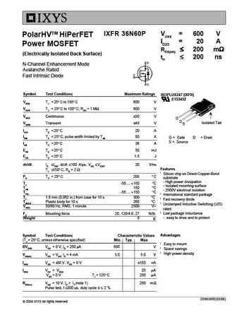
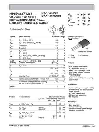
IXFR 36N60P VDSS = 600 V PolarHVTM HiPerFET ID25 = 20 A Power MOSFET RDS(on) 200 m (Electrically Isolated Back Surface) trr 200 ns N-Channel Enhancement Mode Avalanche Rated Fast Intrinsic Diode Symbol Test Conditions Maximum Ratings ISOPLUS247 (IXFR) E153432 VDSS TJ = 25 C to 150 C 600 V VDGR TJ = 25 C to 15
ixgh16n60c2d1.pdf

HiPerFASTTM IGBTs VCES = 600V IXGA16N60C2D1 C2-Class High Speed IC110 = 16A IXGP16N60C2D1 w/ Diode VCE(sat) 3.0V IXGH16N60C2D1 tfi(typ) = 33ns TO-263 AA (IXGA) G E C (Tab) Symbol Test Conditions Maximum Ratings TO-220AB (IXGP) VCES TJ = 25 C to 150 C 600 V VCGR TJ = 25 C to 150 C, RGE = 1M 600 V VGES Continuous 20 V VGEM Transient 30 V G C C
ixgp16n60c2d1.pdf
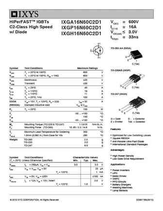
HiPerFASTTM IGBTs VCES = 600V IXGA16N60C2D1 C2-Class High Speed IC110 = 16A IXGP16N60C2D1 w/ Diode VCE(sat) 3.0V IXGH16N60C2D1 tfi(typ) = 33ns TO-263 AA (IXGA) G E C (Tab) Symbol Test Conditions Maximum Ratings TO-220AB (IXGP) VCES TJ = 25 C to 150 C 600 V VCGR TJ = 25 C to 150 C, RGE = 1M 600 V VGES Continuous 20 V VGEM Transient 30 V G C C
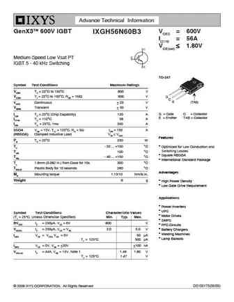
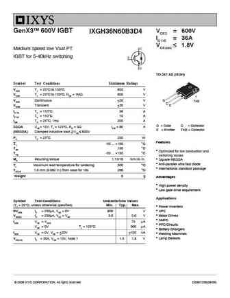
ixgh56n60b3.pdf
Advance Technical Information GenX3TM 600V IGBT VCES = 600V IXGH56N60B3 IC110 = 56A VCE(sat) 1.80V Medium-Speed Low Vsat PT IGBT 5 - 40 kHz Switching TO-247 Symbol Test Conditions Maximum Ratings VCES TC = 25 C to 150 C 600 V G VCGR TJ = 25 C to 150 C, RGE = 1M 600 V G CD ES (TAB) VGES Continuous 20 V VGEM Transient 30 V G = Gate C = Collecto
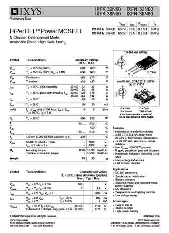
ixfk32n60 ixfn32n60 ixfk36n60 ixfn36n60.pdf
IXFK 32N60 IXFN 32N60 IXFK 36N60 IXFN 36N60 Preliminary Data VDSS ID25 RDS(on) trr IXFK/FN 36N60 600V 36A 0.18 250ns HiPerFETTM Power MOSFET IXFK/FN 32N60 600V 32A 0.25 250ns N-Channel Enhancement Mode Avalanche Rated, High dv/dt, Low trr TO-264 AA (IXFK) Symbol Test Conditions Maximum Ratings IXFK IXFN VDSS TJ = 25 C to 150 C 600 600 V G VDGR TJ = 25 C to 150 C; RGS = 1
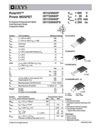
ixfh26n60p ixft26n60p ixfv26n60p.pdf
IXFH26N60P VDSS = 600 V PolarHVTM IXFT26N60P ID25 = 26 A Power MOSFET IXFV26N60P RDS(on) 270 m N-Channel Enhancement Mode IXFV26N60PS trr 200 ns Fast Recovery Diode Avalanche Rated Symbol Test Conditions Maximum Ratings TO-247 (IXFH) VDSS TJ = 25 C to 150 C 600 V VDGR TJ = 25 C to 150 C; RGS = 1 M 600 V VGSS Contin
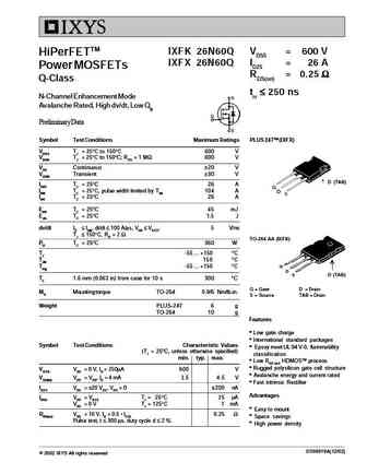
ixfa16n60p3 ixfh16n60p3 ixfp16n60p3.pdf
Advance Technical Information Polar3 TM HiPerFETTM VDSS = 600V IXFA16N60P3 Power MOSFETs ID25 = 16A IXFP16N60P3 RDS(on) 440m IXFH16N60P3 N-Channel Enhancement Mode TO-263 AA (IXFA) Avalanche Rated Fast Intrinsic Rectifier G S D (Tab) TO-220AB (IXFP) Symbol Test Conditions Maximum Ratings VDSS TJ = 25 C to 150 C 600 V VDGR TJ = 25 C to 15
ixgh56n60b3d1.pdf
VCES = 600V GenX3TM 600V IGBT IXGH56N60B3D1 IC110 = 56A VCE(sat) 1.8V Medium speed low Vsat PT IGBTs 5-40 kHz switching TO-247 (IXGH) Symbol Test Conditions Maximum Ratings VCES TC = 25 C to 150 C 600 V VCGR TJ = 25 C to 150 C, RGE = 1M 600 V VGES Continuous 20 V VGEM Transient 30 V G IC110 TC = 110 C 56 A C (TAB) E ICM TC = 25 C, 1ms 350 A
ixgh56n60a3.pdf
Advance Technical Information GenX3TM 600V IGBT VCES = 600V IXGH56N60A3 IC110 = 56A VCE(sat) 1.35V Ultra-Low Vsat PT IGBT for up to 5 kHz Switching TO-247 Symbol Test Conditions Maximum Ratings VCES TC = 25 C to 150 C 600 V G VCGR TJ = 25 C to 150 C, RGE = 1M 600 V G CD ES (TAB) VGES Continuous 20 V VGEM Transient 30 V G = Gate C = Collector
ixtt26n60p ixtv26n60p ixtv26n60ps ixth26n60p ixtq26n60p.pdf
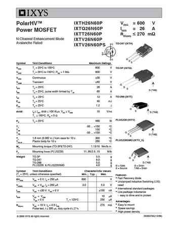
IXTH26N60P VDSS = 600 V PolarHVTM IXTQ26N60P ID25 = 26 A Power MOSFET IXTT26N60P RDS(on) 270 m N-Channel Enhancement Mode IXTV26N60P Avalanche Rated TO-247 (IXTH) IXTV26N60PS G D S Symbol Test Conditions Maximum Ratings VDSS TJ = 25 C to 150 C 600 V TO-3P (IXTQ) VDGR TJ = 25 C to 150 C; RGS = 1 M 600 V VGSS Continuous 30 V VGSM Tran
ixga16n60c2d1.pdf

HiPerFASTTM IGBTs VCES = 600V IXGA16N60C2D1 C2-Class High Speed IC110 = 16A IXGP16N60C2D1 w/ Diode VCE(sat) 3.0V IXGH16N60C2D1 tfi(typ) = 33ns TO-263 AA (IXGA) G E C (Tab) Symbol Test Conditions Maximum Ratings TO-220AB (IXGP) VCES TJ = 25 C to 150 C 600 V VCGR TJ = 25 C to 150 C, RGE = 1M 600 V VGES Continuous 20 V VGEM Transient 30 V G C C
ixfh36n60p ixft36n60p ixfk36n60p.pdf
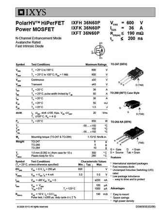
IXFH 36N60P VDSS = 600 V PolarHVTM HiPerFET IXFK 36N60P ID25 = 36 A Power MOSFET IXFT 36N60P RDS(on) 190 m N-Channel Enhancement Mode trr 200 ns Avalanche Rated Fast Intrinsic Diode TO-247 (IXFH) Symbol Test Conditions Maximum Ratings VDSS TJ = 25 C to 150 C 600 V VDGR TJ = 25 C to 150 C; RGS = 1 M 600 V
ixga16n60b2.pdf
HiPerFASTTM IGBTs VCES = 600V IXGA16N60B2 B2-Class High Speed IC110 = 16A IXGP16N60B2 VCE(sat) 2.3V tfi(typ) = 70ns TO-263 AA (IXGA) Symbol Test Conditions Maximum Ratings G E VCES TJ = 25 C to 150 C 600 V C (Tab) VCGR TJ = 25 C to 150 C, RGE = 1M 600 V VGES Continuous 20 V TO-220AB (IXGP) VGEM Transient 30 V IC25 TC = 25 C40 A IC110 TC = 110
ixgh36n60b3d4.pdf
VCES = 600V GenX3TM 600V IGBT IXGH36N60B3D4 IC110 = 36A VCE(sat) 1.8V Medium speed low Vsat PT IGBT for 5-40kHz switching TO-247 AD (IXGH) Symbol Test Conditions Maximum Ratings VCES TJ = 25 C to 150 C 600 V VCGR TJ = 25 C to 150 C, RGE = 1M 600 V VGES Continuous 20 V G TAB C VGEM Transient 30 V E IC110 TC = 110 C 36 A IF110 TC = 110 C 10 A
ixsh16n60u1.pdf
IXSH 16N60U1 VCES = 600V Low VCE(sat) IGBT IC25 = 16A with Diode VCE(sat)typ = 1.8V Short Circuit SOA Capability Preliminary data Symbol Test Conditions Maximum Ratings TO-247 AD VCES TJ = 25 C to 150 C 600 V VCGR TJ = 25 C to 150 C; RGE = 1 MW 600 V VGES Continuous 20 V C (TAB) G VGEM Transient 30 V C E IC25 TC = 25 C32 A IC90 TC = 90 C16 A G = Gate, C = Collecto
ixfk26n60q ixfx26n60q.pdf
IXFK 26N60Q VDSS = 600 V HiPerFETTM IXFX 26N60Q ID25 = 26 A Power MOSFETs RDS(on) = 0.25 Q-Class trr 250 ns N-Channel Enhancement Mode Avalanche Rated, High dv/dt, Low Qg Preliminary Data Symbol Test Conditions Maximum Ratings PLUS 247TM (IXFX) VDSS TJ = 25 C to 150 C 600 V VDGR TJ = 25 C to 150 C; RGS = 1 M 600 V VGS Conti
ixgc16n60c2d1.pdf
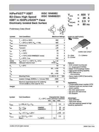
IXGC 16N60C2 HiPerFASTTM IGBT VCES = 600 V IXGC 16N60C2D1 C2-Class High Speed IC25 = 20 A IGBT in ISOPLUS220TM Case VCE(sat) = 3.0 V Electrically Isolated Back Surface tfi(typ) = 35 ns Preliminary Data Sheet D1 Symbol Test Conditions Maximum Ratings ISOPLUS 220TM (IXGC) E153432 VCES TJ = 25 C to 150 C 600 V VCGR TJ = 25 C to 150 C; RGE = 1 M 600 V VGES Continuous 20 V
ixgh16n60b2d1.pdf
HiPerFASTTM IGBTs VCES = 600V IXGA16N60B2D1 B2-Class High Speed IC110 = 16A IXGP16N60B2D1 w/ Diode VCE(sat) 2.3V IXGH16N60B2D1 tfi(typ) = 70ns TO-263 AA (IXGA) G E C (Tab) Symbol Test Conditions Maximum Ratings TO-220AB (IXGP) VCES TJ = 25 C to 150 C 600 V VCGR TJ = 25 C to 150 C, RGE = 1M 600 V VGES Continuous 20 V VGEM Transient 30 V G C C (
ixgh36n60b3.pdf
Advance Technical Information GenX3TM 600V IGBT VCES = 600V IXGH36N60B3 IC110 = 36A VCE(sat) 1.8V Medium-Speed Low-Vsat PT IGBT for 5 - 40kHz Switching TO-247 Symbol Test Conditions Maximum Ratings VCES TJ = 25 C to 150 C 600 V G VCGR TJ = 25 C to 150 C, RGE = 1M 600 V C Tab E VGES Continuous 20 V VGEM Transient 30 V IC25 TC = 25 C 92 A
ixgc16n60c2.pdf

IXGC 16N60C2 HiPerFASTTM IGBT VCES = 600 V IXGC 16N60C2D1 C2-Class High Speed IC25 = 20 A IGBT in ISOPLUS220TM Case VCE(sat) = 3.0 V Electrically Isolated Back Surface tfi(typ) = 35 ns Preliminary Data Sheet D1 Symbol Test Conditions Maximum Ratings ISOPLUS 220TM (IXGC) E153432 VCES TJ = 25 C to 150 C 600 V VCGR TJ = 25 C to 150 C; RGE = 1 M 600 V VGES Continuous 20 V
ixgh36n60b3c1.pdf
Preliminary Technical Information GenX3TM 600V IGBT VCES = 600V IXGH36N60B3C1 w/ SiC Anti-Parallel IC110 = 36A Diode VCE(sat) 1.8V tfi(typ) = 100ns Medium Speed Low Vsat PT IGBT for 5 - 40kHz Switching TO-247 Symbol Test Conditions Maximum Ratings VCES TJ = 25 C to 150 C 600 V G (TAB) VCGR TJ = 25 C to 150 C, RGE = 1M 600 V C E VGES Continuous 20
ixgh36n60a3.pdf

Preliminary Technical Information IXGA36N60A3 VCES = 600V GenX3TM 600V IGBT IXGP36N60A3 IC110 = 36A IXGH36N60A3 VCE(sat) 1.4V Ultra Low Vsat PT IGBT for up to 5kHz switching TO-263 (IXGA) G Symbol Test Conditions Maximum Ratings E (TAB) VCES TC = 25 C to 150 C 600 V TO-220 (IXGP) VCGR TJ = 25 C to 150 C, RGE = 1M 600 V VGES Continuous 20 V VGE
ixgh36n60a3d4.pdf
Preliminary Technical Information VCES = 600V GenX3TM 600V IGBT IXGH36N60A3D4 with Diode IC110 = 36A VCE(sat) 1.4V Ultra Low Vsat PT IGBT for up to 5kHz switching TO-247 (IXGH) Symbol Test Conditions Maximum Ratings VCES TC = 25 C to 150 C 600 V VCGR TJ = 25 C to 150 C, RGE = 1M 600 V VGES Continuous 20 V G VGEM Transient 30 V C (TAB) E IC1
ixfh26n60q ixft26n60q.pdf
IXFH 26N60Q VDSS = 600 V HiPerFETTM IXFT 26N60Q ID25 = 26 A Power MOSFETs RDS(on) = 0.25 Q-Class trr 250 ns N-Channel Enhancement Mode Avalanche Rated, High dv/dt, Low Qg Symbol Test Conditions Maximum Ratings TO-247 AD (IXFH) VDSS TJ = 25 C to 150 C 600 V VDGR TJ = 25 C to 150 C; RGS = 1 M 600 V (TAB) VGS Continuous 20 V
ixgc16n60b2d1.pdf
IXGC 16N60B2 HiPerFASTTM IGBT VCES = 600 V IXGC 16N60B2D1 B2-Class High Speed IC25 = 28 A IGBT in ISOPLUS220TM Case VCE(sat) = 2.3 V Electrically Isolated Back Surface tfi(typ) = 80 ns Preliminary Data Sheet D1 Symbol Test Conditions Maximum Ratings ISOPLUS 220TM (IXGC) E153432 VCES TJ = 25 C to 150 C 600 V VCGR TJ = 25 C to 150 C; RGE = 1 M 600 V VGES Continuous 20 V
ixgc16n60b2.pdf

IXGC 16N60B2 HiPerFASTTM IGBT VCES = 600 V IXGC 16N60B2D1 B2-Class High Speed IC25 = 28 A IGBT in ISOPLUS220TM Case VCE(sat) = 2.3 V Electrically Isolated Back Surface tfi(typ) = 80 ns Preliminary Data Sheet D1 Symbol Test Conditions Maximum Ratings ISOPLUS 220TM (IXGC) E153432 VCES TJ = 25 C to 150 C 600 V VCGR TJ = 25 C to 150 C; RGE = 1 M 600 V VGES Continuous 20 V
ixgp16n60b2.pdf

HiPerFASTTM IGBTs VCES = 600V IXGA16N60B2 B2-Class High Speed IC110 = 16A IXGP16N60B2 VCE(sat) 2.3V tfi(typ) = 70ns TO-263 AA (IXGA) Symbol Test Conditions Maximum Ratings G E VCES TJ = 25 C to 150 C 600 V C (Tab) VCGR TJ = 25 C to 150 C, RGE = 1M 600 V VGES Continuous 20 V TO-220AB (IXGP) VGEM Transient 30 V IC25 TC = 25 C40 A IC110 TC = 110
ixgh36n60b3d1.pdf
GenX3TM 600V IGBT VCES = 600V IXGH36N60B3D1 w/ Diode IC110 = 36A VCE(sat) 1.8V Medium-Speed Low-Vsat PT IGBT for 5 - 40kHz Switching TO-247 Symbol Test Conditions Maximum Ratings VCES TJ = 25 C to 150 C 600 V G VCGR TJ = 25 C to 150 C, RGE = 1M 600 V C (TAB) E VGES Continuous 20 V VGEM Transient 30 V IC110 TC = 110 C 36 A G = Gate C = Col
ixgp16n60b2d1.pdf

HiPerFASTTM IGBTs VCES = 600V IXGA16N60B2D1 B2-Class High Speed IC110 = 16A IXGP16N60B2D1 w/ Diode VCE(sat) 2.3V IXGH16N60B2D1 tfi(typ) = 70ns TO-263 AA (IXGA) G E C (Tab) Symbol Test Conditions Maximum Ratings TO-220AB (IXGP) VCES TJ = 25 C to 150 C 600 V VCGR TJ = 25 C to 150 C, RGE = 1M 600 V VGES Continuous 20 V VGEM Transient 30 V G C C (
ixga36n60a3.pdf
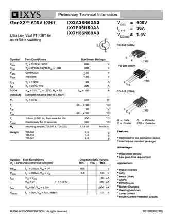
Preliminary Technical Information IXGA36N60A3 VCES = 600V GenX3TM 600V IGBT IXGP36N60A3 IC110 = 36A IXGH36N60A3 VCE(sat) 1.4V Ultra Low Vsat PT IGBT for up to 5kHz switching TO-263 (IXGA) G Symbol Test Conditions Maximum Ratings E (TAB) VCES TC = 25 C to 150 C 600 V TO-220 (IXGP) VCGR TJ = 25 C to 150 C, RGE = 1M 600 V VGES Continuous 20 V VGE
fqp6n60c fqpf6n60c.pdf

Is Now Part of To learn more about ON Semiconductor, please visit our website at www.onsemi.com Please note As part of the Fairchild Semiconductor integration, some of the Fairchild orderable part numbers will need to change in order to meet ON Semiconductor s system requirements. Since the ON Semiconductor product management systems do not have the ability to manage part nomenclatur
fcp36n60n fcpf36n60nt.pdf

Is Now Part of To learn more about ON Semiconductor, please visit our website at www.onsemi.com Please note As part of the Fairchild Semiconductor integration, some of the Fairchild orderable part numbers will need to change in order to meet ON Semiconductor s system requirements. Since the ON Semiconductor product management systems do not have the ability to manage part nomenclatur
ndf06n60z ndp06n60z.pdf
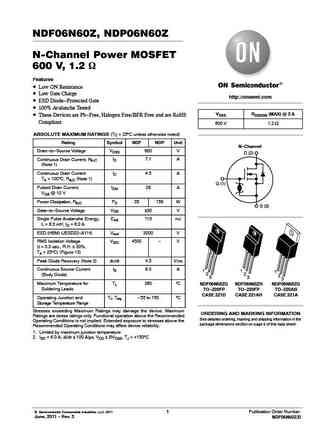
NDF06N60Z, NDP06N60Z N-Channel Power MOSFET 600 V, 1.2 W Features Low ON Resistance Low Gate Charge http //onsemi.com ESD Diode-Protected Gate 100% Avalanche Tested VDSS RDS(ON) (MAX) @ 3 A These Devices are Pb-Free, Halogen Free/BFR Free and are RoHS Compliant 600 V 1.2 ABSOLUTE MAXIMUM RATINGS (TC = 25 C unless otherwise noted) Rating Symbol NDF NDP Unit
fcp16n60n fcpf16n60nt.pdf

Is Now Part of To learn more about ON Semiconductor, please visit our website at www.onsemi.com Please note As part of the Fairchild Semiconductor integration, some of the Fairchild orderable part numbers will need to change in order to meet ON Semiconductor s system requirements. Since the ON Semiconductor product management systems do not have the ability to manage part nomenclatur
fcp16n60 fcpf16n60.pdf

Is Now Part of To learn more about ON Semiconductor, please visit our website at www.onsemi.com Please note As part of the Fairchild Semiconductor integration, some of the Fairchild orderable part numbers will need to change in order to meet ON Semiconductor s system requirements. Since the ON Semiconductor product management systems do not have the ability to manage part nomenclatur
fch76n60nf.pdf

Is Now Part of To learn more about ON Semiconductor, please visit our website at www.onsemi.com Please note As part of the Fairchild Semiconductor integration, some of the Fairchild orderable part numbers will need to change in order to meet ON Semiconductor s system requirements. Since the ON Semiconductor product management systems do not have the ability to manage part nomenclatur
6n60z.pdf
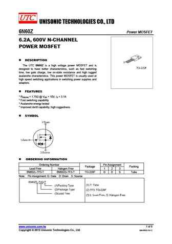
UNISONIC TECHNOLOGIES CO., LTD 6N60Z Power MOSFET 6.2A, 600V N-CHANNEL POWER MOSFET DESCRIPTION The UTC 6N60Z is a high voltage power MOSFET and is designed to have better characteristics, such as fast switching time, low gate charge, low on-state resistance and high rugged avalanche characteristics. This power MOSFET is usually used at high speed switching applications in
6n60kl-tms-t 6n60kg-tms-t 6n60kl-tms2-t 6n60kg-tms2-t 6n60kl-tms4-t 6n60kg-tms4-t 6n60kl-tn3-r 6n60kg-tn3-r 6n60kl-tnd-r 6n60kg-tnd-r 6n60kg-tm3-t.pdf

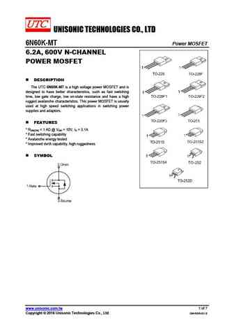
UNISONIC TECHNOLOGIES CO., LTD 6N60K-MT Power MOSFET 6.2A, 600V N-CHANNEL POWER MOSFET DESCRIPTION The UTC 6N60K-MT is a high voltage power MOSFET and is designed to have better characteristics, such as fast switching time, low gate charge, low on-state resistance and have a high rugged avalanche characteristics. This power MOSFET is usually used at high speed switching ap
6n60kl-ta3-t 6n60kg-ta3-t 6n60kl-tf3-t 6n60kg-tf3-t 6n60kl-tf1-t 6n60kg-tf1-t 6n60kl-tf2-t 6n60kg-tf2-t 6n60kl-tf3-t 6n60kg-tf3-t 6n60kl-tm3-t.pdf
UNISONIC TECHNOLOGIES CO., LTD 6N60K-MT Power MOSFET 6.2A, 600V N-CHANNEL POWER MOSFET DESCRIPTION The UTC 6N60K-MT is a high voltage power MOSFET and is designed to have better characteristics, such as fast switching time, low gate charge, low on-state resistance and have a high rugged avalanche characteristics. This power MOSFET is usually used at high speed switching ap
apt106n60b2c6.pdf
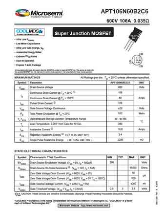
APT106N60B2C6 600V 106A 0.035 COOLMOS Power Semiconductors Super Junction MOSFET Ultra Low RDS(ON) Low Miller Capacitance Ultra Low Gate Charge, Qg Avalanche Energy Rated D Extreme dv/dt Rated Dual die (parallel) G Popular T-MAX Package S Unless stated otherwise, Microsemi discrete MOSFETs contain a single MOSFET die. This device is made with
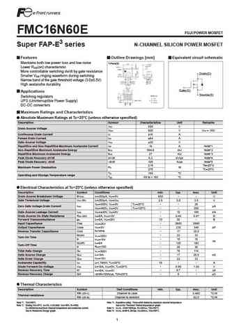
fmc16n60es.pdf
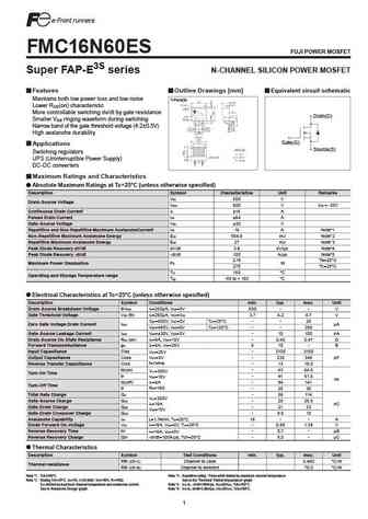
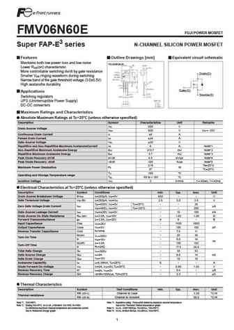
FMC16N60ES FUJI POWER MOSFET Super FAP-E3S series N-CHANNEL SILICON POWER MOSFET Features Outline Drawings [mm] Equivalent circuit schematic Maintains both low power loss and low noise T-Pack(S) Lower R (on) characteristic DS More controllable switching dv/dt by gate resistance Drain(D) Smaller V ringing waveform during switching GS Narrow band of the gate threshold voltage (4.2 0.5
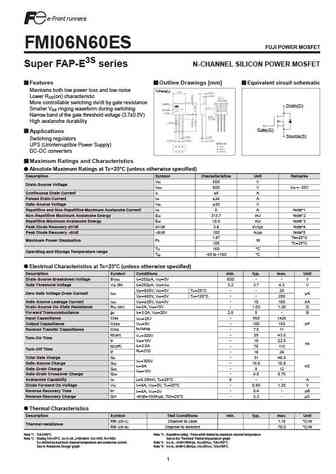
fmp16n60es.pdf
FMP16N60ES FUJI POWER MOSFET Super FAP-E3S series N-CHANNEL SILICON POWER MOSFET Features Outline Drawings [mm] Equivalent circuit schematic Maintains both low power loss and low noise TO-220AB Lower R (on) characteristic DS More controllable switching dv/dt by gate resistance Drain(D) Smaller V ringing waveform during switching GS Narrow band of the gate threshold voltage (4.2 0.5V
fmv16n60es.pdf
FMV16N60ES FUJI POWER MOSFET Super FAP-E3S series N-CHANNEL SILICON POWER MOSFET Features Outline Drawings [mm] Equivalent circuit schematic Maintains both low power loss and low noise TO-220F(SLS) Lower R (on) characteristic DS More controllable switching dv/dt by gate resistance Drain(D) Smaller V ringing waveform during switching GS Narrow band of the gate threshold voltage (4.2
fmi16n60es.pdf

FMI16N60ES FUJI POWER MOSFET Super FAP-E3S series N-CHANNEL SILICON POWER MOSFET Features Outline Drawings [mm] Equivalent circuit schematic Maintains both low power loss and low noise T-Pack(L) Lower R (on) characteristic DS More controllable switching dv/dt by gate resistance Drain(D) Smaller V ringing waveform during switching GS Narrow band of the gate threshold voltage (4.2 0.5
fmp06n60es.pdf

FMP06N60ES FUJI POWER MOSFET Super FAP-E3S series N-CHANNEL SILICON POWER MOSFET Features Outline Drawings [mm] Equivalent circuit schematic Maintains both low power loss and low noise TO-220AB Lower R (on) characteristic DS More controllable switching dv/dt by gate resistance Drain(D) Smaller V ringing waveform during switching GS Narrow band of the gate threshold voltage (3.7 0.5V
fmi16n60e.pdf
FMI16N60E FUJI POWER MOSFET Super FAP-E3 series N-CHANNEL SILICON POWER MOSFET Features Outline Drawings [mm] Equivalent circuit schematic Maintains both low power loss and low noise T-Pack(L) Lower R (on) characteristic DS More controllable switching dv/dt by gate resistance Drain(D) Smaller V ringing waveform during switching GS Narrow band of the gate threshold voltage (3.0 0.5V)
fmv16n60e.pdf

FMV16N60E FUJI POWER MOSFET Super FAP-E3 series N-CHANNEL SILICON POWER MOSFET Features Outline Drawings [mm] Equivalent circuit schematic Maintains both low power loss and low noise TO-220F(SLS) Lower R (on) characteristic DS More controllable switching dv/dt by gate resistance Drain(D) Smaller V ringing waveform during switching GS Narrow band of the gate threshold voltage (3.0 0.
fmc16n60e.pdf
FMC16N60E FUJI POWER MOSFET Super FAP-E3 series N-CHANNEL SILICON POWER MOSFET Features Outline Drawings [mm] Equivalent circuit schematic Maintains both low power loss and low noise T-Pack(S) Lower R (on) characteristic DS More controllable switching dv/dt by gate resistance Drain(D) Smaller V ringing waveform during switching GS Narrow band of the gate threshold voltage (3.0 0.5V)
fmc06n60es.pdf

FMC06N60ES FUJI POWER MOSFET Super FAP-E3S series N-CHANNEL SILICON POWER MOSFET Features Outline Drawings [mm] Equivalent circuit schematic Maintains both low power loss and low noise T-Pack(S) Lower R (on) characteristic DS More controllable switching dv/dt by gate resistance Drain(D) Smaller V ringing waveform during switching GS Narrow band of the gate threshold voltage (3.7 0.5
fmi06n60es.pdf
FMI06N60ES FUJI POWER MOSFET Super FAP-E3S series N-CHANNEL SILICON POWER MOSFET Features Outline Drawings [mm] Equivalent circuit schematic Maintains both low power loss and low noise T-Pack(L) Lower R (on) characteristic DS More controllable switching dv/dt by gate resistance Drain(D) Smaller V ringing waveform during switching GS Narrow band of the gate threshold voltage (3.7 0.5
fmh16n60es.pdf
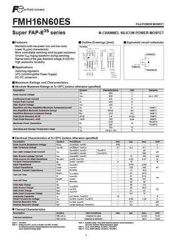
FMH16N60ES FUJI POWER MOSFET Super FAP-E3S series N-CHANNEL SILICON POWER MOSFET Features Outline Drawings [mm] Equivalent circuit schematic Maintains both low power loss and low noise TO-3P(Q) Lower R (on) characteristic DS More controllable switching dv/dt by gate resistance Drain(D) Smaller V ringing waveform during switching GS Narrow band of the gate threshold voltage (4.2 0.5V
fml16n60es.pdf
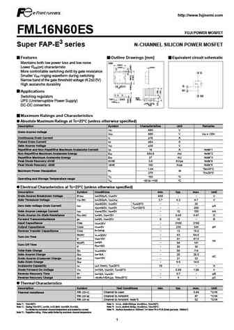
http //www.fujisemi.com FML16N60ES FUJI POWER MOSFET Super FAP-E3 series N-CHANNEL SILICON POWER MOSFET Features Outline Drawings [mm] Equivalent circuit schematic Maintains both low power loss and low noise TFP 9.0 0.2 7.0 0.2 0.4 0.1 Lower R (on) characteristic DS 4 More controllable switching dv/dt by gate resistance 4 D Smaller V ringing waveform during switching GS Narrow
fmp06n60e.pdf

FMP06N60E FUJI POWER MOSFET Super FAP-E3 series N-CHANNEL SILICON POWER MOSFET Features Outline Drawings [mm] Equivalent circuit schematic Maintains both low power loss and low noise TO-220AB Lower R (on) characteristic DS More controllable switching dv/dt by gate resistance Drain(D) Smaller V ringing waveform during switching GS Narrow band of the gate threshold voltage (3.0 0.5V)
fmv06n60e.pdf
FMV06N60E FUJI POWER MOSFET Super FAP-E3 series N-CHANNEL SILICON POWER MOSFET Features Outline Drawings [mm] Equivalent circuit schematic Maintains both low power loss and low noise TO-220F(SLS) Lower R (on) characteristic DS More controllable switching dv/dt by gate resistance Drain(D) Smaller V ringing waveform during switching GS Narrow band of the gate threshold voltage (3.0 0.
fmp16n60e.pdf

FMP16N60E FUJI POWER MOSFET Super FAP-E3 series N-CHANNEL SILICON POWER MOSFET Features Outline Drawings [mm] Equivalent circuit schematic Maintains both low power loss and low noise TO-220AB Lower R (on) characteristic DS More controllable switching dv/dt by gate resistance Drain(D) Smaller V ringing waveform during switching GS Narrow band of the gate threshold voltage (3.0 0.5V)
ssq6n60.pdf
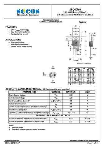
SSQ6N60 2.6A, 600V, RDS(ON) 1500m N-Ch Enhancement Mode Power MOSFET Elektronische Bauelemente RoHS Compliant Product A suffix of -C specifies halogen free TO-220P D FEATURES C Low RDS(on) Technology. B R Low thermal impedance. T Fast switching speed. A E S G APPLICATIONS F I Electronic ballast. H J Electronic transformer K
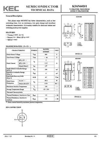
kf6n60p-f.pdf
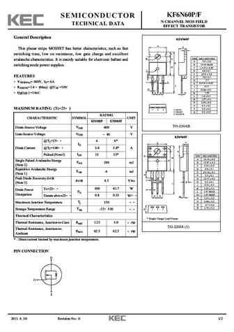
KF6N60P/F SEMICONDUCTOR N CHANNEL MOS FIELD TECHNICAL DATA EFFECT TRANSISTOR General Description KF6N60P This planar stripe MOSFET has better characteristics, such as fast switching time, low on resistance, low gate charge and excellent avalanche characteristics. It is mainly suitable for electronic ballast and switching mode power supplies. FEATURES VDSS(Min.)= 600V, ID= 6A
kf6n60d-i.pdf
KF6N60D/I SEMICONDUCTOR N CHANNEL MOS FIELD TECHNICAL DATA EFFECT TRANSISTOR General Description KF6N60D This planar stripe MOSFET has better characteristics, such as fast switching time, low on resistance, low gate charge and excellent A K DIM MILLIMETERS L C D _ A 6.60 + 0.20 avalanche characteristics. It is mainly suitable for electronic ballast and _ B 6.10 + 0.20 _ C 5.
h06n60.pdf
Spec. No. MOS200402 HI-SINCERITY Issued Date 2004.04.01 Revised Date 2005.03.10 MICROELECTRONICS CORP. Page No. 1/6 H06N60 Series Pin Assignment H06N60 Series Tab 3-Lead Plastic TO-263 N-Channel Power Field Effect Transistor Package Code U Pin 1 Gate Pin 2 & Tab Drain 3 2 Pin 3 Source 1 Description Tab This high voltage MOSFET uses an advanced termination scheme t
afn06n60t220ft afn06n60t251t.pdf
AFN06N60 Alfa-MOS 600V / 6A N-Channel Technology Enhancement Mode MOSFET General Description Features AFN06N60 is an N-channel enhancement mode Power 600V/3A,RDS(ON)=1.5 (MAX)@VGS=10V MOSFET which is produced using VDMOS technology. The Low gate charge improved planar stripe cell and the improved guard ring Low Crss terminal have been especially tailored to minimize on-state
sdu06n60 sdd06n60.pdf
Green Product SDU/D06N60 a S mHop Microelectronics C orp. Ver 1.0 N-Channel Logic Level Enhancement Mode Field Effect Transistor FEATURES PRODUCT SUMMARY Super high dense cell design for low RDS(ON). VDSS ID RDS(ON) ( ) Typ Rugged and reliable. 600V 6A 1.18 @ VGS=10V Suface Mount Package. D G G S S SDU SERIES SDD SERIES SDD SERIES TO-252(D-PAK) TO-251S(I-PAK) TO-251L(I-PAK)
sdf06n60 sdp06n60.pdf
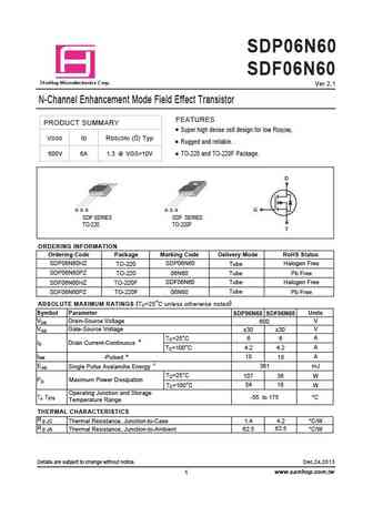
SDP06N60 SDF06N60 a S mHop Microelectronics C orp. Ver 2.1 N-Channel Enhancement Mode Field Effect Transistor FEATURES PRODUCT SUMMARY Super high dense cell design for low RDS(ON). RDS(ON) ( ) Typ VDSS ID Rugged and reliable. 600V 6A 1.3 @ VGS=10V TO-220 and TO-220F Package. D G D S G D S G SDP SERIES SDF SERIES TO-220 TO-220F S ORDERING INFORMATION Ordering Code Package Mar
ssf6n60g.pdf
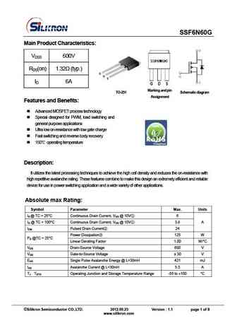
SSF6N60G Main Product Characteristics VDSS 600V RDS(on) 1.32 (typ.) ID 6A TO-251 Marking a nd p in Sche ma ti c di agr a m Assignment Features and Benefits Advanced MOSFET process technology Special designed for PWM, load switching and general purpose applications Ultra low on-resistance with low gate charge Fast switching and reverse body recovery
ftp06n60c fta06n60c.pdf
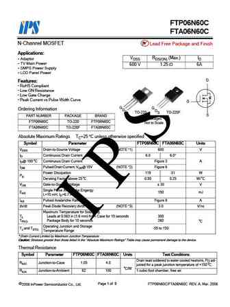
FTP06N60C FTA06N60C Pb N-Channel MOSFET Lead Free Package and Finish Applications VDSS RDS(ON) (Max.) ID Adaptor TV Main Power 600 V 1.25 6A SMPS Power Supply LCD Panel Power D Features RoHS Compliant Low ON Resistance Low Gate Charge Peak Current vs Pulse Width Curve G G G Ordering Information DS DS TO-220F TO-220 S PART NUMBER
brd6n60.pdf
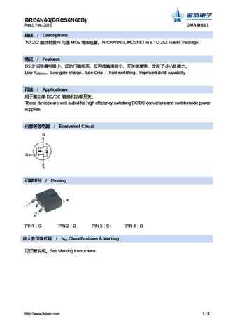
BRD6N60(BRCS6N60D) Rev.C Feb.-2015 DATA SHEET / Descriptions TO-252 N MOS N-CHANNEL MOSFET in a TO-252 Plastic Package. / Features DS dv/dt Low RDS(ON) Low gate charge Low Crss Fast switching Improved dv/dt capability.
brf6n60.pdf
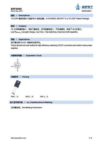
BRF6N60 Rev.D Nov.-2015 DATA SHEET / Descriptions TO-220F N MOS N-CHANNEL MOSFET in a TO-220F Plastic Package. / Features DS dv/dt Low RDS(ON), Low gate charge, Low Crss , Fast switching, Improved dv/dt capability. / App
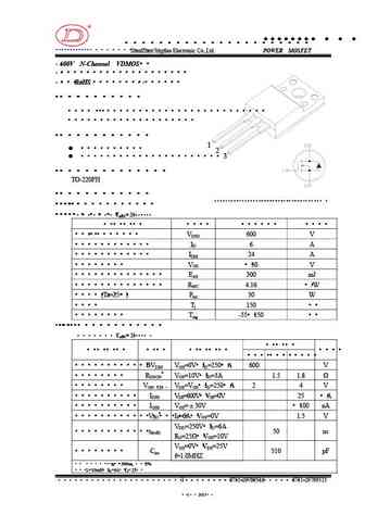
6n60a 6n60af 6n60f 6n60g.pdf
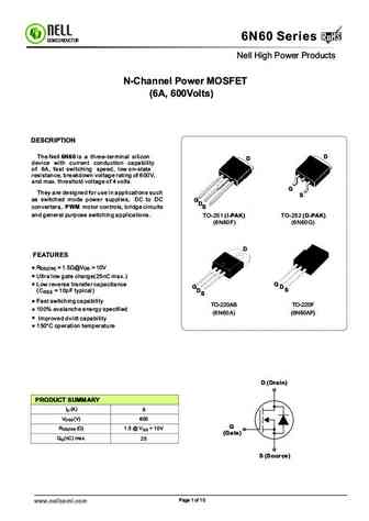
RoHS 6N60 Series RoHS SEMICONDUCTOR Nell High Power Products N-Channel Power MOSFET (6A, 600Volts) DESCRIPTION The Nell 6N60 is a three-terminal silicon D D device with current conduction capability of 6A, fast switching speed, low on-state resistance, breakdown voltage rating of 600V, and max. threshold voltage of 4 volts. G They are designed for use in applications such
16n60a 16n60af 16n60b.pdf
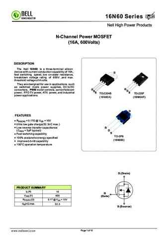
RoHS 16N60 Series RoHS SEMICONDUCTOR Nell High Power Products N-Channel Power MOSFET (16A, 600Volts) DESCRIPTION The Nell 16N60 is a three-terminal silicon device with current conduction capability of 16A, D fast switching speed, low on-state resistance, breakdown voltage rating of 600V ,and max. threshold voltage of 4 volts. They are designed for use in applications. such a
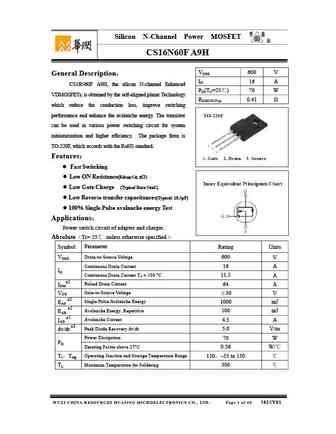
cs16n60 a8h.pdf

Silicon N-Channel Power MOSFET R CS16N60 A8H VDSS 600 V General Description ID 16 A CS16N60 A8, the silicon N-channel Enhanced PD(TC=25 ) 180 W VDMOSFETs, is obtained by the self-aligned planar Technology RDS(ON)Typ 0.41 which reduce the conduction loss, improve switching performance and enhance the avalanche energy. The transistor can be used in various pow
cs6n60f a9h.pdf

Silicon N-Channel Power MOSFET R CS6N60F A9H General Description VDSS 600 V CS6N60F A9H, the silicon N-channel Enhanced ID 6 A PD(TC=25 ) 34 W VDMOSFETs, is obtained by the self-aligned planar Technology RDS(ON)Typ 1.4 which reduce the conduction loss, improve switching performance and enhance the avalanche energy. The transistor can be used in various pow
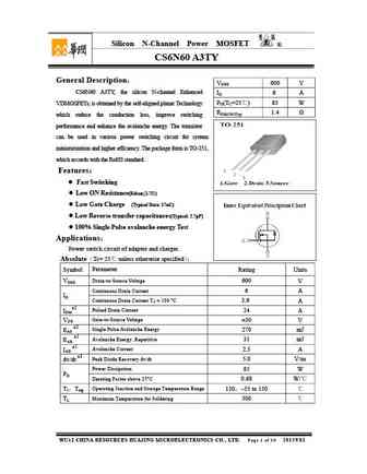
cs6n60f a9ty.pdf

Silicon N-Channel Power MOSFET R CS6N60F A9TY General Description VDSS 600 V CS6N60F A9TY, the silicon N-channel Enhanced ID 6 A PD(TC=25 ) 34 W VDMOSFETs, is obtained by the self-aligned planar Technology RDS(ON)Typ 1.4 which reduce the conduction loss, improve switching performance and enhance the avalanche energy. The transistor can be used in various po
cs6n60 a4d.pdf

Silicon N-Channel Power MOSFET R CS6N60 A4D General Description VDSS 600 V CS6N60 A4D, the silicon N-channel Enhanced ID 6 A PD(TC=25 ) 95 W VDMOSFETs, is obtained by the self-aligned planar Technology RDS(ON)Typ 1.0 which reduce the conduction loss, improve switching performance and enhance the avalanche energy. The transistor can be used in various power
cs6n60 a3d.pdf
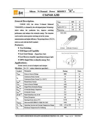
Silicon N-Channel Power MOSFET R CS6N60 A3D General Description VDSS 600 V CS6N60 A3D, the silicon N-channel Enhanced ID 6 A PD(TC=25 ) 95 W VDMOSFETs, is obtained by the self-aligned planar Technology RDS(ON)Typ 1.0 which reduce the conduction loss, improve switching performance and enhance the avalanche energy. The transistor can be used in various power sw
cs6n60 a8h.pdf
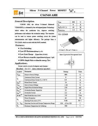
Silicon N-Channel Power MOSFET R CS6N60 A8H General Description VDSS 600 V CS6N60 A8H, the silicon N-channel Enhanced ID 6 A PD(TC=25 ) 85 W VDMOSFETs, is obtained by the self-aligned planar Technology RDS(ON)Typ 1.4 which reduce the conduction loss, improve switching performance and enhance the avalanche energy. The transistor can be used in various power sw
cs6n60 a3ty.pdf
Silicon N-Channel Power MOSFET R CS6N60 A3TY General Description VDSS 600 V CS6N60 A3TY, the silicon N-channel Enhanced ID 6 A PD(TC=25 ) 85 W VDMOSFETs, is obtained by the self-aligned planar Technology RDS(ON)Typ 1.4 which reduce the conduction loss, improve switching performance and enhance the avalanche energy. The transistor can be used in various power
cs6n60 a3hdy.pdf

Silicon N-Channel Power MOSFET R CS6N60 A3HDY General Description VDSS 600 V CS6N60 A3HDY, the silicon N-channel Enhanced ID 6 A PD(TC=25 ) 95 W VDMOSFETs, is obtained by the self-aligned planar Technology RDS(ON)Typ 1.0 which reduce the conduction loss, improve switching performance and enhance the avalanche energy. The transistor can be used in various pow
cs6n60 a4ty.pdf

Silicon N-Channel Power MOSFET R CS6N60 A4TY General Description VDSS 600 V CS6N60 A4TY, the silicon N-channel Enhanced ID 6 A PD(TC=25 ) 85 W VDMOSFETs, is obtained by the self-aligned planar Technology RDS(ON)Typ 1.4 which reduce the conduction loss, improve switching performance and enhance the avalanche energy. The transistor can be used in various pow
cs16n60f a9h.pdf
Silicon N-Channel Power MOSFET R CS16N60F A9H VDSS 600 V General Description ID 16 A CS16N60F A9H, the silicon N-channel Enhanced PD(TC=25 ) 70 W VDMOSFETs, is obtained by the self-aligned planar Technology RDS(ON)Typ 0.41 which reduce the conduction loss, improve switching performance and enhance the avalanche energy. The transistor can be used in various
cs6n60 a7h.pdf
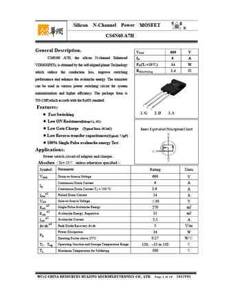
Silicon N-Channel Power MOSFET R CS6N60 A7H General Description VDSS 600 V CS6N60 A7H, the silicon N-channel Enhanced ID 6 A PD(TC=25 ) 34 W VDMOSFETs, is obtained by the self-aligned planar Technology RDS(ON)Typ 1.4 which reduce the conduction loss, improve switching performance and enhance the avalanche energy. The transistor can be used in various power
cs6n60 a4h.pdf
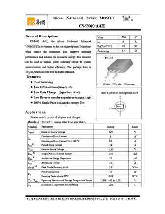
Silicon N-Channel Power MOSFET R CS6N60 A4H General Description VDSS 600 V CS6N60 A4H, the silicon N-channel Enhanced ID 6 A PD(TC=25 ) 85 W VDMOSFETs, is obtained by the self-aligned planar Technology RDS(ON)Typ 1.4 which reduce the conduction loss, improve switching performance and enhance the avalanche energy. The transistor can be used in various power
cs6n60f a9h-g.pdf
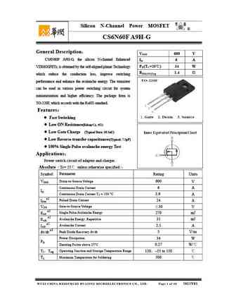
Silicon N-Channel Power MOSFET R CS6N60F A9H-G General Description VDSS 600 V CS6N60F A9H-G, the silicon N-channel Enhanced ID 6 A PD(TC=25 ) 34 W VDMOSFETs, is obtained by the self-aligned planar Technology RDS(ON)Typ 1.4 which reduce the conduction loss, improve switching performance and enhance the avalanche energy. The transistor can be used in various
cm6n60.pdf
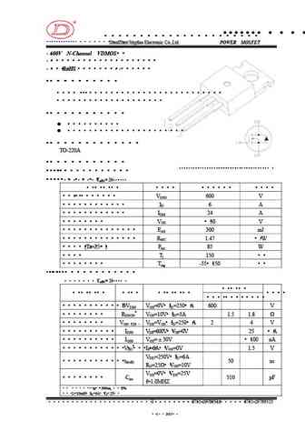
R C66 MN0 www.jdsemi.cn ShenZhen Jingdao Electronic Co.,Ltd. POWER MOSFET 600V N-Channel VDMOS RoHS 1 LD E 2 3
ndt6n60p.pdf
DIP Type MOSFET N-Channel MOSFET NDT6N60P TO-251 Features VDS (V) = 600V 1 2 3 ID = 6.2 A (VGS = 10V) RDS(ON) 1.5 (VGS = 10V) Fast switching capability Low reverse transfer Capacitance 1 3 2 Drain Unit mm Gate Source Absolute Maximum Ratings Ta = 25 Parameter Symbol Rating Unit Drain-Source Voltage VDS 600 V Gate-Source Voltage V
svf6n60f svf6n60dtr svf6n60fq.pdf
SVF6N60F/D/FQ 6A 600V N 2 SVF6N60F/D/FQ N MOS F-CellTM VDMOS 1 1 3 TO-252-2L 3
svf6n60mj svf6n60f svf6n60d.pdf
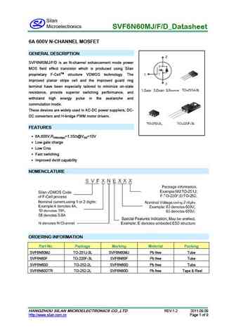
SVF6N60MJ/F/D_Datasheet 6A 600V N-CHANNEL MOSFET GENERAL DESCRIPTION SVF6N60MJ/F/D is an N-channel enhancement mode power MOS field effect transistor which is produced using Silan proprietary F-CellTM structure VDMOS technology. The improved planar stripe cell and the improved guard ring terminal have been especially tailored to minimize on-state resistance, provide superior swit
mdf6n60bth.pdf
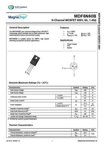
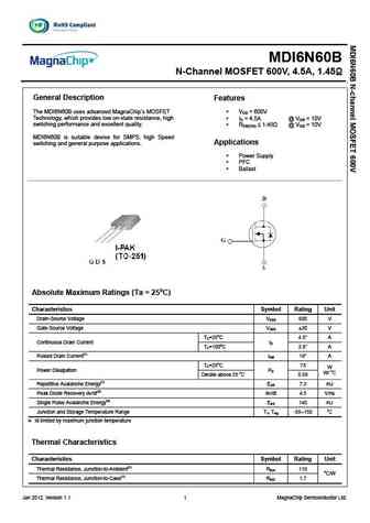
MDF6N60B N-Channel MOSFET 600V, 6A, 1.45 General Description Features The MDF6N60B uses advanced MagnaChip s MOSFET VDS = 600V Technology, which provides low on-state resistance, high ID = 6.0A @ VGS = 10V switching performance and excellent quality. RDS(ON) 1.4 @ VGS = 10V MDF6N60B is suitable device for SMPS, high Speed Applications switch
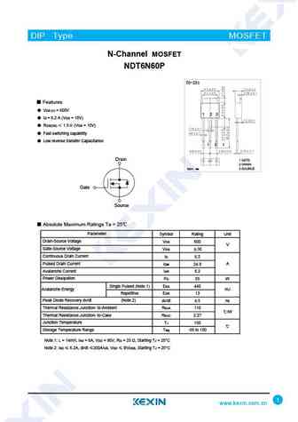
mdf6n60th mdp6n60th.pdf
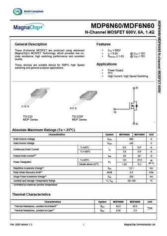
MDP6N60/MDF6N60 N-Channel MOSFET 600V, 6A, 1.4 General Description Features These N-channel MOSFET are produced using advanced V = 600V DS MagnaChip s MOSFET Technology, which provides low on- I = 6.0A @ V = 10V D GS state resistance, high switching performance and excellent R 1.4 @ V = 10V DS(ON) GS quality. Applications These devices are suitable device for SM
mdd6n60grh.pdf
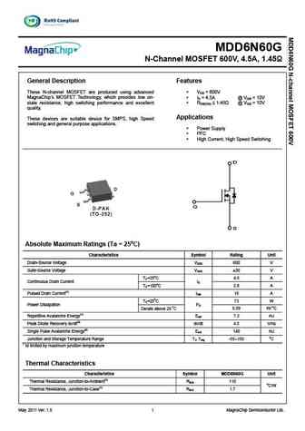
MDD6N60G N-Channel MOSFET 600V, 4.5A, 1.45 General Description Features These N-channel MOSFET are produced using advanced VDS = 600V MagnaChip s MOSFET Technology, which provides low on- ID = 4.5A @ VGS = 10V state resistance, high switching performance and excellent RDS(ON) 1.45 @ VGS = 10V quality. Applications These devices are suitable device for SMPS, high S
mdi6n60bth.pdf
MDI6N60B N-Channel MOSFET 600V, 4.5A, 1.45 General Description Features The MDI6N60B uses advanced MagnaChip s MOSFET VDS = 600V Technology, which provides low on-state resistance, high ID = 4.5A @ VGS = 10V switching performance and excellent quality. RDS(ON) 1.45 @ VGS = 10V MDI6N60B is suitable device for SMPS, high Speed Applications swi
msf6n60.pdf

MSF6N60 N-Channel Enhancement Mode Power MOSFET Description The MSF6N60 is a N-channel enhancement-mode MOSFET , providing the designer with the best combination of fast switching, ruggedized device design, low on-resistance and cost effectiveness. The TO-220F package is universally preferred for all commercial-industrial applications Features Low On Resistance Sim
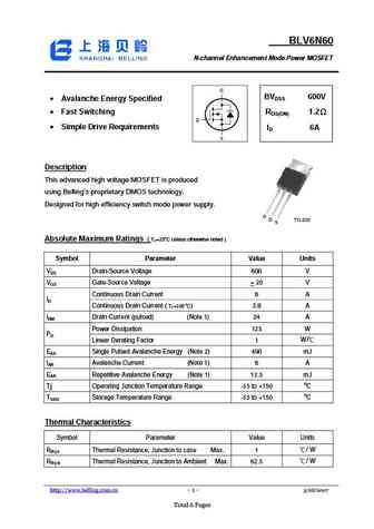
blv6n60.pdf
BLV6N60 N-channel Enhancement Mode Power MOSFET 600V DSS Avalanche Energy Specified BV Fast Switching RDS(ON) 1.2 Simple Drive Requirements ID 6A Description This advanced high voltage MOSFET is produced using Belling s proprietary DMOS technology. Designed for high efficiency switch mode power supply. Absolute Maximum Ratings ( TC=25oC unless
ctm06n60.pdf
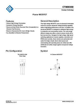
CTM06N60 CTM06N60 Crownpo Technology Crownpo Technology Power MOSFET Features General Description Robust High Voltage Termination This high voltage MOSFET uses an advanced termination Avalanche Energy Specified scheme to provide enhanced voltage-blocking capability Source-to-Drain Diode Recovery Time Comparable to a without degrading performance over time. In addition,
hy6n60d.pdf
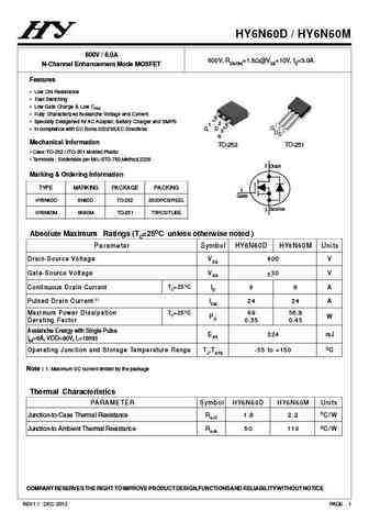
HY6N60D / HY6N60M 600V / 6.0A 600V, RDS(ON)=1.8 @VGS=10V, ID=3.0A N-Channel Enhancement Mode MOSFET Features Low ON Resistance Fast Switching Low Gate Charge & Low CRSS Fully Characterized Avalanche Voltage and Current Specially Desigened for AC Adapter, Battery Charger and SMPS 2 1 1 D G 2 In compliance with EU RoHs 2002/95/EC Directives G 3 DS3 S Mec
hy6n60t.pdf
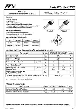
HY6N60T / HY6N60FT 600V / 6.0A 600V, RDS(ON)=1.8 @VGS=10V, ID=3.0A N-Channel Enhancement Mode MOSFET Features Low ON Resistance Fast Switching Low Gate Charge & Low CRSS Fully Characterized Avalanche Voltage and Current Specially Desigened for AC Adapter, Battery Charger and SMPS 1 1 2 2 In compliance with EU RoHs 2002/95/EC Directives G G 3 3 D D S
cs6n60f.pdf
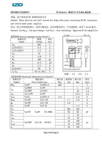
BRF6N60(CS6N60F) N-Channel MOSFET/N MOS DC/DC Purpose These devices are well suited for high efficiency switching DC/DC converters and switch mode power supplies. DS dv/dt Features Low R Low gate charge Low C
nceap016n60vd.pdf
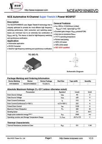
http //www.ncepower.com NCEAP016N60VD NCE Automotive N-Channel Super Trench II Power MOSFET Description General Features The NCEAP016N60VD uses Super Trench II technology that is V =60V,I =315A(Silicon Limited) DS D uniquely optimized to provide the most efficient high frequency R =1.1m , typical @ V =10V DS(ON) GS switching performance. Both conduction and switching power
ncep016n60vd.pdf

NCEP016N60VD NCE N-Channel Super Trench II Power MOSFET Description The series of devices uses Super Trench II technology that is General Features uniquely optimized to provide the most efficient high frequency V =60V,I =305A DS D switching performance. Both conduction and switching power R =1.1m , typical @ V =10V DS(ON) GS losses are minimized due to an extremely low combinati
pta26n60.pdf
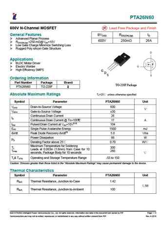
PTA26N60 600V N-Channel MOSFET General Features BVDSS RDS(ON),typ. ID Advanced Planar Process 600V 250m 26A RDS(ON),typ.=250 m @VGS=10V Low Gate Charge Minimize Switching Loss Rugged Poly silicon Gate Structure Applications BLDC Motor Driver Electric Welder High Efficiency SMPS G D S Ordering Information Part Number Package Brand TO-220F Package P
ptp16n60 pta16n60.pdf
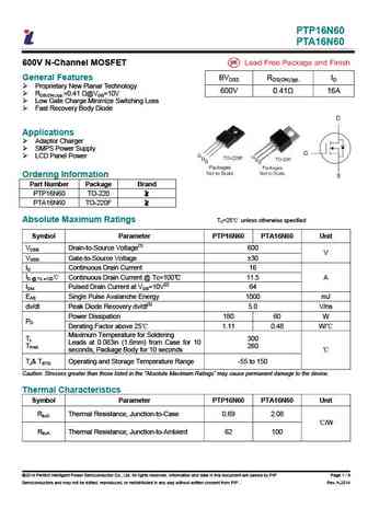
PTP16N60 PTA16N60 600V N-Channel MOSFET General Features BVDSS RDS(ON),typ. ID Proprietary New Planar Technology 600V 0.41 16A RDS(ON),typ.=0.41 @VGS=10V Low Gate Charge Minimize Switching Loss Fast Recovery Body Diode Applications Adaptor Charger SMPS Power Supply LCD Panel Power Ordering Information Part Number Package Brand PTP16N60
ptw36n60.pdf
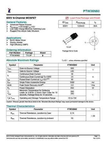
PTW36N60 600V N-Channel MOSFET General Features BVDSS RDS(ON),typ. ID Advanced Planar Process 600V 120m 36A RDS(ON),typ.=120 m @VGS=10V Low Gate Charge Minimize Switching Loss Rugged Poly silicon Gate Structure Applications BLDC Motor Driver G D Electric Welder S High Efficiency SMPS TO-3P Ordering Information Package Not to Scale Part Number Pack
swf16n60d.pdf
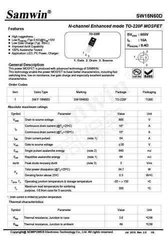
SW16N60D N-channel Enhanced mode TO-220F MOSFET Features TO-220F BVDSS 600V High ruggedness Low RDS(ON) (Typ 0.4 )@VGS=10V ID 16A Low Gate Charge (Typ 68nC) RDS(ON) 0.4 Improved dv/dt Capability 100% Avalanche Tested 2 1 Application LED, PC Power, Charger 2 3 1 1. Gate 2. Drain 3. Source General Description 3 This pow
swf6n60d swd6n60d swn6n60d.pdf
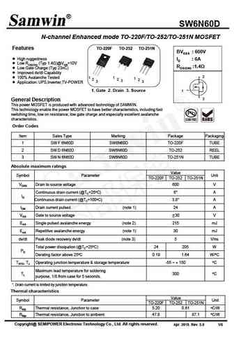
SW6N60D N-channel Enhanced mode TO-220F/TO-252/TO-251N MOSFET Features TO-220F TO-252 TO-251N BVDSS 600V High ruggedness ID 6A Low RDS(ON) (Typ 1.4 )@VGS=10V RDS(ON) 1.4 Low Gate Charge (Typ 23nC) Improved dv/dt Capability 2 100% Avalanche Tested 1 1 1 2 2 2 3 3 3 Application UPS,Inverter,TV-POWER 1. Gate 2. Drain 3. Source
swf6n60k.pdf
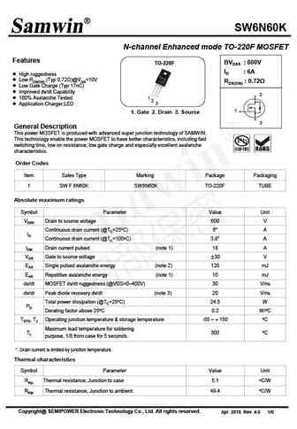
SW6N60K N-channel Enhanced mode TO-220F MOSFET Features BVDSS 600V TO-220F ID 6A High ruggedness Low RDS(ON) (Typ 0.72 )@VGS=10V RDS(ON) 0.72 Low Gate Charge (Typ 17nC) Improved dv/dt Capability 2 100% Avalanche Tested 1 2 3 Application Charger,LED 1 1. Gate 2. Drain 3. Source 3 General Description This power MOSFET is
swf16n60k.pdf
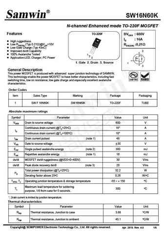
SW16N60K N-channel Enhanced mode TO-220F MOSFET Features TO-220F BVDSS 600V ID 16A High ruggedness Low RDS(ON) (Typ 0.21 )@VGS=10V RDS(ON) 0.21 Low Gate Charge (Typ 43nC) Improved dv/dt Capability 2 100% Avalanche Tested 1 2 Application LED, Charger, PC Power 3 1. Gate 2. Drain 3. Source 1 3 General Description This power MO
srm6n60.pdf
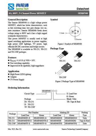
Datasheet 6A, 600V, N-Channel Power MOSFET SRM6N60 General Description Symbol The Sanrise SRM6N60 is a high voltage power MOSFET, which has better characteristics, such as fast switching time, low gate charge, low on- state resistance. Sanrise SRM6N60 break down voltage rating is 600V and it has a high rugged avalanche characteristics. This power MOSFET is usually used at high
hfp6n60u.pdf
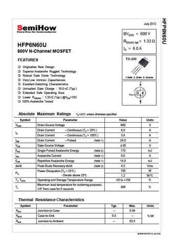
July 2012 BVDSS = 600 V RDS(on) typ HFP6N60U ID = 6.0 A 600V N-Channel MOSFET TO-220 FEATURES Originative New Design Superior Avalanche Rugged Technology 1 2 3 Robust Gate Oxide Technology 1.Gate 2. Drain 3. Source Very Low Intrinsic Capacitances Excellent Switching Characteristics Unrivalled Gate Charge 16.0 nC (Typ.) Extended Safe Operating Area
hfd6n60u.pdf
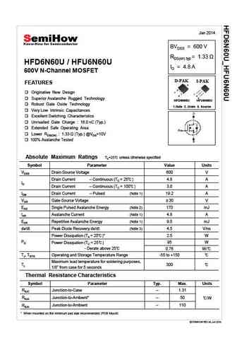
Jan 2014 BVDSS = 600 V RDS(on) typ HFD6N60U / HFU6N60U ID = 4.8 A 600V N-Channel MOSFET D-PAK I-PAK FEATURES 2 1 Originative New Design 1 3 2 3 Superior Avalanche Rugged Technology HFD6N60U HFU6N60U Robust Gate Oxide Technology 1.Gate 2. Drain 3. Source Very Low Intrinsic Capacitances Excellent Switching Characteristics Unrivalled Gate Charge 16.0 n
hfs6n60u.pdf
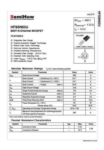
July 2012 BVDSS = 600 V RDS(on) typ HFS6N60U ID = 6.0 A 600V N-Channel MOSFET TO-220F FEATURES Originative New Design Superior Avalanche Rugged Technology 1 2 3 Robust Gate Oxide Technology 1.Gate 2. Drain 3. Source Very Low Intrinsic Capacitances Excellent Switching Characteristics Unrivalled Gate Charge 16.0 nC (Typ.) Extended Safe Operating Area
tman16n60.pdf
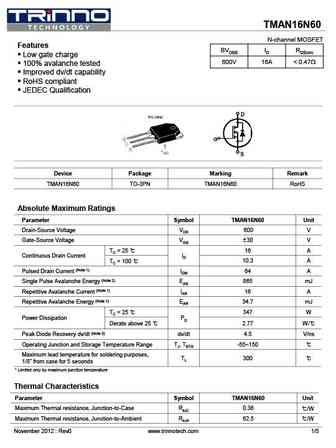
TMAN16N60 N-channel MOSFET Features BVDSS ID RDS(on) Low gate charge 600V 16A
tman16n60a.pdf
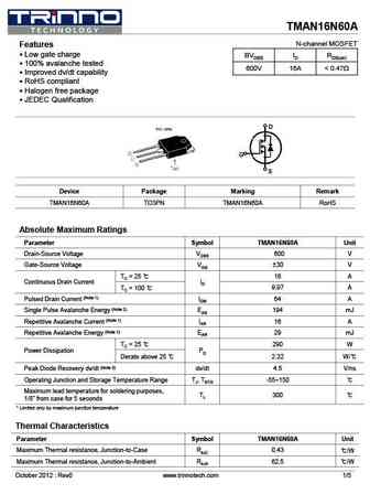
TMAN16N60A N-channel MOSFET Features Low gate charge BVDSS ID RDS(on) 100% avalanche tested 600V 16A
tmp16n60a tmpf16n60a.pdf
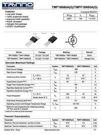
TMP16N60A(G)/TMPF16N60A(G) Features N-channel MOSFET Low gate charge BVDSS ID RDS(on) 100% avalanche tested 600V 16A
tmp16n60 tmpf16n60.pdf
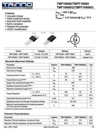
TMP16N60/TMPF16N60 TMP16N60G/TMPF16N60G VDSS = 660 V @Tjmax Features ID = 16A Low gate charge RDS(on) = 0.47 W(max) @ VGS= 10 V 100% avalanche tested Improved dv/dt capability RoHS compliant Halogen free package JEDEC Qualification D G S Device Package Marking Remark TMP16N60 / TMPF16N60 TO-220 / TO-220F TMP16N60 / TMPF16N60 RoHS TMP16N60G / TMPF16N60G
tsf16n60mr.pdf
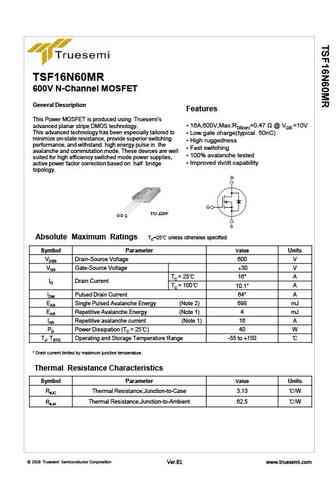
TSF16N60MR 600V N-Channel MOSFET General Description Features This Power MOSFET is produced using Truesemi s 16A,600V,Max.RDS(on)=0.47 @ VGS =10V advanced planar stripe DMOS technology. This advanced technology has been especially tailored to Low gate charge(typical 50nC) minimize on-state resistance, provide superior switching High ruggedness performance, a
wml26n60c4 wmk26n60c4 wmn26n60c4 wmm26n60c4 wmo26n60c4 wmj26n60c4.pdf

WML26N60C4, WMO26N6 WM C4 W 60C4, MK26N60C WMN2 MJ26N60C 26N60C4, WMM26N60C4, WM C4 600V 0.16 S T V Super Junction Power MOSFET Descrip ption WMOSTM C4 is Wa 4th generation super ayon s n junction MOSFET fa that is utilizing charge M amily S balance te or extremely esistance echnology fo y low on-re S D D G G G S D G and low ga charge performanc WMOSTM
wml26n60c4 wmo26n60c4 wmk26n60c4 wmn26n60c4 wmm26n60c4 wmj26n60c4.pdf

WML26N60C4, WMO26N6 WM C4 W 60C4, MK26N60C WMN2 MJ26N60C 26N60C4, WMM26N60C4, WM C4 600V 0.16 S T V Super Junction Power MOSFET Descrip ption WMOSTM C4 is Wa 4th generation super ayon s n junction MOSFET fa that is utilizing charge M amily S balance te or extremely esistance echnology fo y low on-re S D D G G G S D G and low ga charge performanc WMOSTM
wml26n60f2 wmo26n60f2 wmk26n60f2 wmn26n60f2 wmm26n60f2 wmj26n60f2.pdf
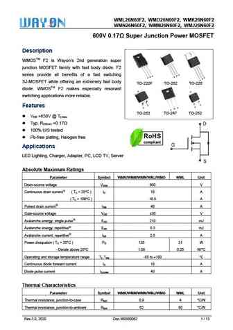
WML2 N60F2, WM F2 26N60F2, WMO26N MK26N60F WMN2 N60F2, WM F2 26N60F2, WMM26N MJ26N60F 600V 0.17 S T V Super Junction Power MOSFET Descrip ption WMOSTM F2 is Wa 2nd generation super ayon s junction MOSFET fam with fa body di F2 M mily ast iode. S series pro all benefits of a fast switching ovide b f s S D D G G G S D G SJ-MOSFE while of an extremely fa
wml36n60f2 wmk36n60f2 wmn36n60f2 wmm36n60f2 wmj36n60f2.pdf

WML36N60F2, WM F2 MK36N60F WMN3 N60F2, WM F2 36N60F2, WMM36N MJ36N60F 600V 0.087 S 0 Super Junction Power MOSFET Descrip ption WMOSTM F2 is Wa 2nd generation super ayon s junction MOSFET fam with fa body di F2 M mily ast iode. S series pro all benefits of a fast switching ovide b f s S D D G G G S D G SJ-MOSFE while of an extremely fa body ET ffering
wml36n60c4 wmk36n60c4 wmn36n60c4 wmm36n60c4 wmj36n60c4.pdf
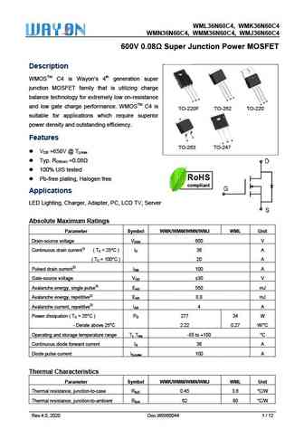
WML36N6 WM C4 60C4, MK36N60C WMN3 MJ36N60C 36N60C4, WMM36N60C4, WM C4 600V 0.08 S T V Super Junction Power MOSFET Descrip ption WMOSTM C4 is Wa 4th generation super ayon s n junction MOSFET fa that is utilizing charge M amily S balance te or extremely esistance echnology fo y low on-re S D D G G G S D G and low ga charge performanc WMOSTM C4 is ate c
cs6n60fa9ty.pdf

Silicon N-Channel Power MOSFET R CS6N60F A9TY General Description VDSS 600 V CS6N60F A9TY, the silicon N-channel Enhanced ID 6 A PD(TC=25 ) 34 W VDMOSFETs, is obtained by the self-aligned planar Technology RDS(ON)Typ 1.4 which reduce the conduction loss, improve switching performance and enhance the avalanche energy. The transistor can be used in various po
cs16n60a8h.pdf
Silicon N-Channel Power MOSFET R CS16N60 A8H VDSS 600 V General Description ID 16 A CS16N60 A8, the silicon N-channel Enhanced PD(TC=25 ) 180 W VDMOSFETs, is obtained by the self-aligned planar Technology RDS(ON)Typ 0.41 which reduce the conduction loss, improve switching performance and enhance the avalanche energy. The transistor can be used in various pow
cs6n60a3ty.pdf

Silicon N-Channel Power MOSFET R CS6N60 A3TY General Description VDSS 600 V CS6N60 A3TY, the silicon N-channel Enhanced ID 6 A PD(TC=25 ) 85 W VDMOSFETs, is obtained by the self-aligned planar Technology RDS(ON)Typ 1.4 which reduce the conduction loss, improve switching performance and enhance the avalanche energy. The transistor can be used in various power
cs6n60a4ty.pdf
Silicon N-Channel Power MOSFET R CS6N60 A4TY General Description VDSS 600 V CS6N60 A4TY, the silicon N-channel Enhanced ID 6 A PD(TC=25 ) 85 W VDMOSFETs, is obtained by the self-aligned planar Technology RDS(ON)Typ 1.4 which reduce the conduction loss, improve switching performance and enhance the avalanche energy. The transistor can be used in various pow
cs6n60a3d.pdf
Silicon N-Channel Power MOSFET R CS6N60 A3D General Description VDSS 600 V CS6N60 A3D, the silicon N-channel Enhanced ID 6 A PD(TC=25 ) 95 W VDMOSFETs, is obtained by the self-aligned planar Technology RDS(ON)Typ 1.0 which reduce the conduction loss, improve switching performance and enhance the avalanche energy. The transistor can be used in various power sw
cs6n60fa9h.pdf
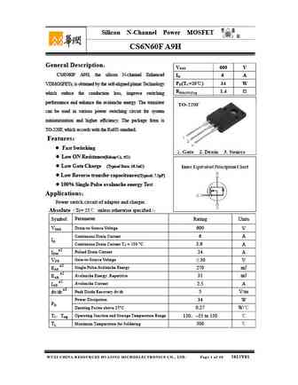
Silicon N-Channel Power MOSFET R CS6N60F A9H General Description VDSS 600 V CS6N60F A9H, the silicon N-channel Enhanced ID 6 A PD(TC=25 ) 34 W VDMOSFETs, is obtained by the self-aligned planar Technology RDS(ON)Typ 1.4 which reduce the conduction loss, improve switching performance and enhance the avalanche energy. The transistor can be used in various pow
cs6n60a4d.pdf
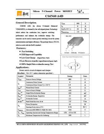
Silicon N-Channel Power MOSFET R CS6N60 A4D General Description VDSS 600 V CS6N60 A4D, the silicon N-channel Enhanced ID 6 A PD(TC=25 ) 95 W VDMOSFETs, is obtained by the self-aligned planar Technology RDS(ON)Typ 1.0 which reduce the conduction loss, improve switching performance and enhance the avalanche energy. The transistor can be used in various power
csfr6n60f csfr6n60k csfr6n60u csfr6n60d.pdf
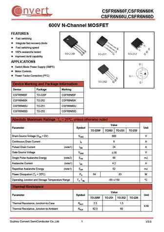
CSFR6N60F,CSFR6N60K nvert Suzhou Convert Semiconductor Co ., Ltd. CSFR6N60U,CSFR6N60D 600V N-Channel MOSFET FEATURES Fast switching Integrate fast recovery diode Fast switching speed 100% avalanche tested Improved dv/dt capability APPLICATIONS Switch Mode Power Supply (SMPS) Motor Controls Power Factor Correction (PFC) Device Marking and Package In
cs16n60f cs16n60p.pdf
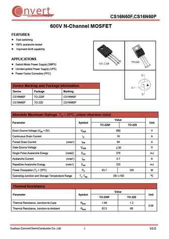
nvert Suzhou Convert Semiconductor Co ., Ltd. CS16N60F,CS16N60P 600V N-Channel MOSFET FEATURES Fast switching 100% avalanche tested Improved dv/dt capability APPLICATIONS Switch Mode Power Supply (SMPS) Uninterruptible Power Supply (UPS) Power Factor Correction (PFC) Device Marking and Package Information Device Package Marking CS16N60F TO-220F CS16N60F CS
fir6n60fg.pdf
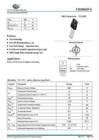
FIR6N60FG N-Channel Power MOSFET PIN Connection TO-220F VDSS 600 V ID 6 A PD(TC=25 ) 85 W RDS(ON) 1.4 G Features D S Fast Switching g Schematic dia ram Low ON Resistance(Rdson 1.6 ) D Low Gate Charge (Typical Data 22nC) Low Reverse transfer capacitances(Typical 14pF) G 100% Single Pulse avalanche energy Test S Marking Diagram Applications Powe
jmpf16n60bj.pdf
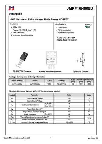
JMPF16N60BJ Description JMP N-channel Enhancement Mode Power MOSFET Features Applications 600V, 16A Load Switch RDS(ON)
jmpc16n60bj.pdf
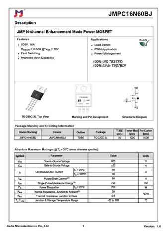
JMPC16N60BJ Description JMP N-channel Enhancement Mode Power MOSFET Features Applications 600V, 16A Load Switch RDS(ON)
lnd16n60 lnc16n60.pdf
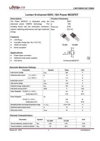
LND16N60/LNC16N60 Lonten N-channel 600V, 16A Power MOSFET Description Product Summary The Power MOSFET is fabricated using the V 600V DSS advanced planer VDMOS technology. The I 16A D resulting device has low conduction resistance, R 0.5 DS(on),max superior switching performance and high avalanche Q 53.2 nC g,typ energy. Features Low R DS(on) Low gate charge (typ. Q = 5
stf6n60m2.pdf
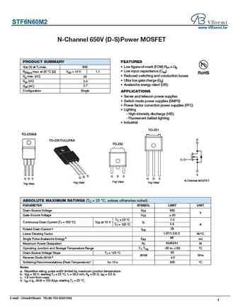
STF6N60M2 www.VBsemi.tw N hannel 650 D S Power MOSFET FEATURES PRODUCT SUMMARY VDS (V) at TJ max. 650 Low figure-of-merit (FOM) Ron x Qg Low input capacitance (Ciss) RDS(on) max. at 25 C ( ) VGS = 10 V 1.1 Reduced switching and conduction losses Qg max. (nC) 25 Ultra low gate charge (Qg) Qgs (nC) 2.0 Avalanche energy rated (UIS) Qgd (nC) 2.7 Configuratio
fqpf6n60c.pdf
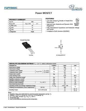
FQPF6N60C www.VBsemi.tw Power MOSFET FEATURES PRODUCT SUMMARY Low Gate Charge Qg Results in Simple Drive VDS (V) 650 Available Requirement RDS(on) ( )VGS = 10 V 2.1 RoHS* Improved Gate, Avalanche and Dynamic dV/dt COMPLIANT Qg (Max.) (nC) 48 Ruggedness Qgs (nC) 12 Fully Characterized Capacitance and Avalanche Voltage and Current Qgd (nC) 19 Compliant to RoHS
hm16n60f.pdf
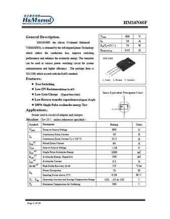
VDSS 600 V General Description ID 16 A HM16N60F, the silicon N-channel Enhanced PD(TC=25 ) 70 W VDMOSFETs, is obtained by the self-aligned planar Technology RDS(ON)Typ 0.41 which reduce the conduction loss, improve switching performance and enhance the avalanche energy. The transistor can be used in various power switching circuit for system miniaturizati
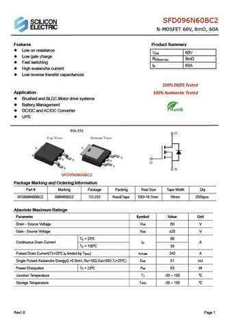
xnf6n60t.pdf
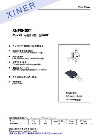
Data Sheet XNF6N60T 600V/6A IGBT /PRODUCT FEATURES 2 + Advanced Trench+FS IGBT technology 1 Low Collector-Emitter Saturation voltage 3 With anti-parallel fast recovery diode TJ = 175 C Maximum junction temperature TJ =
spp06n60c3.pdf
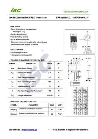
isc N-Channel MOSFET Transistor SPP06N60C3 ISPP06N60C3 FEATURES Static drain-source on-resistance RDS(on) 0.75 Enhancement mode Fast Switching Speed 100% avalanche tested Minimum Lot-to-Lot variations for robust device performance and reliable operation DESCRIPTION Ultra low gate charge High peak current capability ABSOLUTE MAXIMUM RATINGS(T =25 ) a
irfib6n60a.pdf
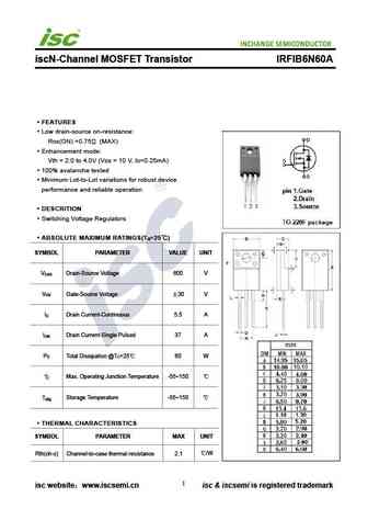
iscN-Channel MOSFET Transistor IRFIB6N60A FEATURES Low drain-source on-resistance RDS(ON) =0.75 (MAX) Enhancement mode Vth = 2.0 to 4.0V (VDS = 10 V, ID=0.25mA) 100% avalanche tested Minimum Lot-to-Lot variations for robust device performance and reliable operation DESCRITION Switching Voltage Regulators ABSOLUTE MAXIMUM RATINGS(T =25 ) a SYMBOL PARAMETER VAL
fcpf16n60.pdf
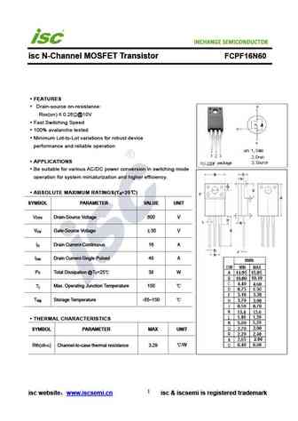
INCHANGE Semiconductor isc N-Channel MOSFET Transistor FCPF16N60 FEATURES Drain-source on-resistance RDS(on) 0.26 @10V Fast Switching Speed 100% avalanche tested Minimum Lot-to-Lot variations for robust device performance and reliable operation APPLICATIONS Be suitable for various AC/DC power conversion in switching mode operation for system miniaturization and
fcpf16n60nt.pdf

isc N-Channel MOSFET Transistor FCPF16N60NT FEATURES With TO-220 packaging High speed switching Low gate input resistance Standard level gate drive Easy to use 100% avalanche tested Minimum Lot-to-Lot variations for robust device performance and reliable operation APPLICATIONS Power supply Switching applications ABSOLUTE MAXIMUM RATINGS(T =25 ) a SYMBOL
spd06n60c3.pdf
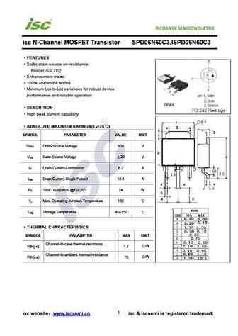
isc N-Channel MOSFET Transistor SPD06N60C3,ISPD06N60C3 FEATURES Static drain-source on-resistance RDS(on) 0.75 Enhancement mode 100% avalanche tested Minimum Lot-to-Lot variations for robust device performance and reliable operation DESCRITION High peak current capability ABSOLUTE MAXIMUM RATINGS(T =25 ) a SYMBOL PARAMETER VALUE UNIT V Drain-Source Voltage
spa06n60c3.pdf
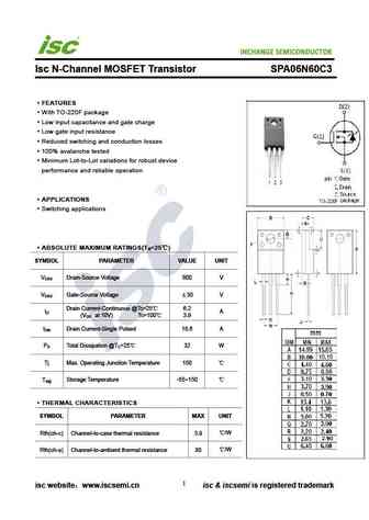
INCHANGE Semiconductor Isc N-Channel MOSFET Transistor SPA06N60C3 FEATURES With TO-220F package Low input capacitance and gate charge Low gate input resistance Reduced switching and conduction losses 100% avalanche tested Minimum Lot-to-Lot variations for robust device performance and reliable operation APPLICATIONS Switching applications ABSOLUTE MAXIMUM RATINGS
irfp26n60l.pdf
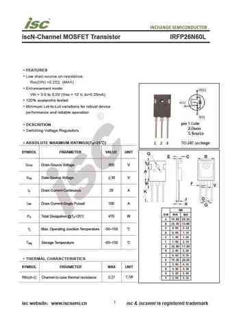
iscN-Channel MOSFET Transistor IRFP26N60L FEATURES Low drain-source on-resistance RDS(ON) =0.25 (MAX) Enhancement mode Vth = 3.0 to 5.0V (VDS = 10 V, ID=0.25mA) 100% avalanche tested Minimum Lot-to-Lot variations for robust device performance and reliable operation DESCRITION Switching Voltage Regulators ABSOLUTE MAXIMUM RATINGS(T =25 ) a SYMBOL PARAMETER VAL
fcp36n60n.pdf
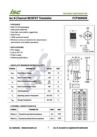
INCHANGE Semiconductor isc N-Channel MOSFET Transistor FCP36N60N FEATURES With TO-220 packaging High speed switching Very high commutation ruggedness Easy to use 100% avalanche tested Minimum Lot-to-Lot variations for robust device performance and reliable operationz APPLICATIONS PFC stages LCD & PDP TV Power supply Switching applications ABSOLUTE MAXIMU
fcp16n60n.pdf
isc N-Channel MOSFET Transistor FCP16N60N FEATURES With TO-220 packaging High speed switching Low gate input resistance Standard level gate drive Easy to use 100% avalanche tested Minimum Lot-to-Lot variations for robust device performance and reliable operation APPLICATIONS Power supply Switching applications ABSOLUTE MAXIMUM RATINGS(T =25 ) a SYMBOL PA
Другие IGBT... 3N65K, 4N65, 4N65Z, 4N65K, 5N65, 5N65K, 6N65, 5N60, IRF830, 6N60Z, 7N60A, 7N60, 7N60Z, 7N60K, 8N60, 10N60, 10N60K
Параметры MOSFET. Взаимосвязь и компромиссы
History: 70N06
🌐 : EN ES РУ

Список транзисторов
Обновления
MOSFET: MSH100N045SA | MSD60P16 | MSD40P45 | MSB100N023 | MS60P03 | MS40P05AU | MS40P05 | MS40N05 | MS34P07 | MS34P01 | MS23P03 | MS23N06A | BPMS04N003M | BPM0405CG | BPM0306CG | BP0405SCG
Popular searches
2n3053 equivalent | 2n3569 | 2sd667 | 2sc1111 | bc239 transistor equivalent | 3sk41 | 2sc2240 transistor | c3198