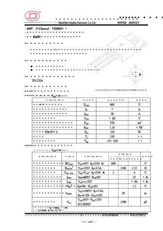
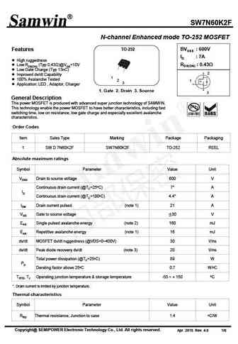
7N60. Аналоги и основные параметры
Наименование производителя: 7N60
Тип транзистора: MOSFET
Полярность: N
Предельные значения
Pd ⓘ - Максимальная рассеиваемая мощность: 142 W
|Vds|ⓘ - Максимально допустимое напряжение сток-исток: 600 V
|Vgs|ⓘ - Максимально допустимое напряжение затвор-исток: 30 V
|Id| ⓘ - Максимально допустимый постоянный ток стока: 7.4 A
Tj ⓘ - Максимальная температура канала: 150 °C
Электрические характеристики
tr ⓘ - Время нарастания: 180 ns
Cossⓘ - Выходная емкость: 125 pf
RDSonⓘ - Сопротивление сток-исток открытого транзистора: 0.83 Ohm
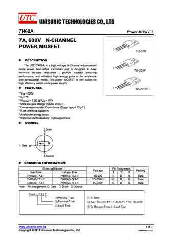
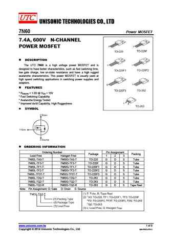
Тип корпуса: TO-220 TO-220F TO-220F1 TO-220F2 TO-262 TO-263
Аналог (замена) для 7N60
- подборⓘ MOSFET транзистора по параметрам
7N60 даташит
7n60.pdf
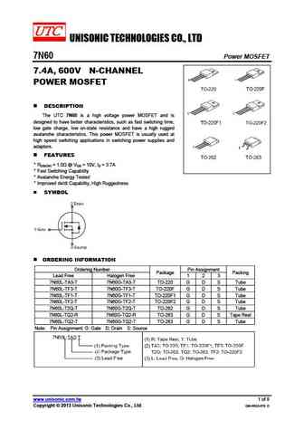
UNISONIC TECHNOLOGIES CO., LTD 7N60 Power MOSFET 7.4A, 600V N-CHANNEL POWER MOSFET DESCRIPTION The UTC 7N60 is a high voltage power MOSFET and is designed to have better characteristics, such as fast switching time, low gate charge, low on-state resistance and have a high rugged avalanche characteristics. This power MOSFET is usually used at high speed switching applicatio
7n60 7n60f.pdf
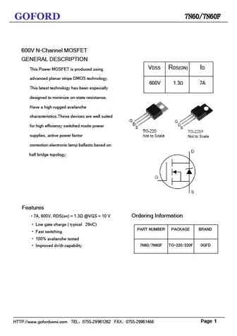
7N60/7N60F GOFORD 600V N-Channel MOSFET GENERAL DESCRIPTION VDSS RDS(ON) ID This Power MOSFET is produced using advanced planar stripe DMOS technology. 600V 1.3 7A This latest technology has been especially designed to minimize on-state resistance, Have a high rugged avalanche characteristics.These devices are well suited for high efficiency switched mode power supplies, active p
7n60.pdf
7N60 www.VBsemi.tw N-Channel 650V (D-S) Power MOSFET FEATURES PRODUCT SUMMARY VDS (V) at TJ max. 650 Low figure-of-merit (FOM) Ron x Qg Low input capacitance (Ciss) RDS(on) max. at 25 C ( ) VGS = 10 V 0.86 43 Reduced switching and conduction losses Qg max. (nC) Ultra low gate charge (Qg) 5 Qgs (nC) Avalanche energy rated (UIS) 22 Qgd (nC) Configuration S
7n60.pdf
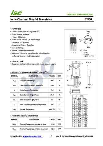
INCHANGE Semiconductor isc N-Channel Mosfet Transistor 7N60 FEATURES Drain Current I = 7.4A@ T =25 D C Drain Source Voltage- V = 600V(Min) DSS Static Drain-Source On-Resistance R = 1.2 (Max) DS(on) Avalanche Energy Specified Fast Switching Simple Drive Requirements Minimum Lot-to-Lot variations for robust device performance and reliable operation DES
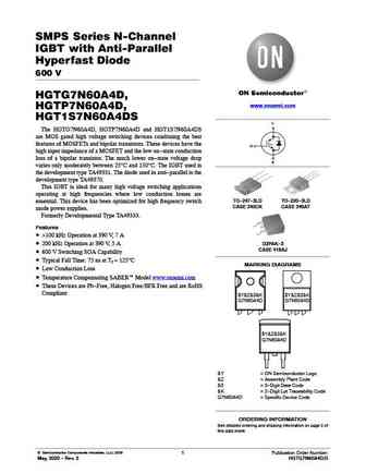
hgtd7n60c3s hgtp7n60c3.pdf

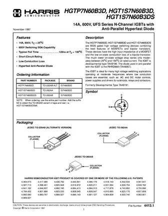
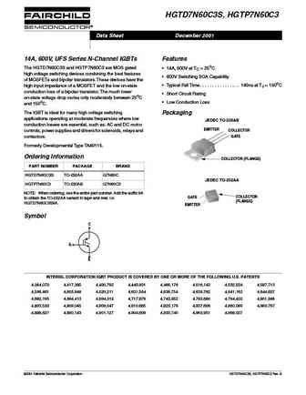
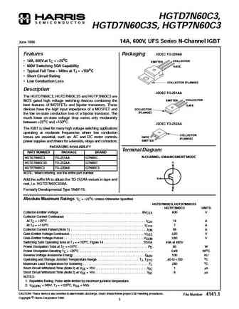
HGTD7N60C3S, HGTP7N60C3 Data Sheet December 2001 14A, 600V, UFS Series N-Channel IGBTs Features The HGTD7N60C3S and HGTP7N60C3 are MOS gated 14A, 600V at TC = 25oC high voltage switching devices combining the best features 600V Switching SOA Capability of MOSFETs and bipolar transistors. These devices have the Typical Fall Time. . . . . . . . . . . . . . . . 140ns at TJ =
hgtp7n60c3d hgt1s7n60c3ds.pdf
HGTP7N60C3D, HGT1S7N60C3DS Data Sheet December 2001 14A, 600V, UFS Series N-Channel IGBT Features with Anti-Parallel Hyperfast Diodes 14A, 600V at TC = 25oC The HGTP7N60C3D and HGT1S7N60C3DS are MOS gated 600V Switching SOA Capability high voltage switching devices combining the best features Typical Fall Time. . . . . . . . . . . . . . . . 140ns at TJ = 150oC of MOSFETs
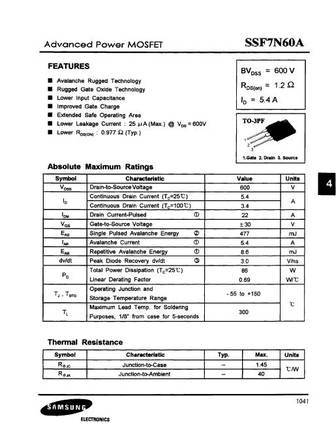
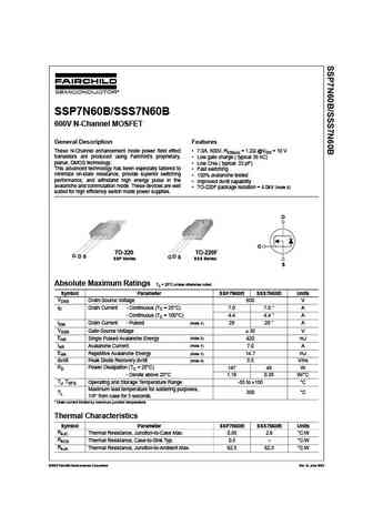
ssf7n60b.pdf
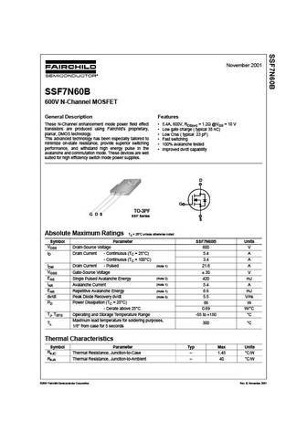
November 2001 SSF7N60B 600V N-Channel MOSFET General Description Features These N-Channel enhancement mode power field effect 5.4A, 600V, RDS(on) = 1.2 @VGS = 10 V transistors are produced using Fairchild s proprietary, Low gate charge ( typical 38 nC) planar, DMOS technology. Low Crss ( typical 23 pF) This advanced technology has been especially tailored to Fast s
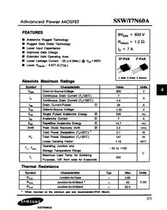
ssw7n60b ssi7n60b.pdf
November 2001 SSW7N60B / SSI7N60B 600V N-Channel MOSFET General Description Features These N-Channel enhancement mode power field effect 7.0A, 600V, RDS(on) = 1.2 @VGS = 10 V transistors are produced using Fairchild s proprietary, Low gate charge ( typical 38 nC) planar, DMOS technology. Low Crss ( typical 23 pF) This advanced technology has been especially tailored to
hgtg27n60c3dr.pdf
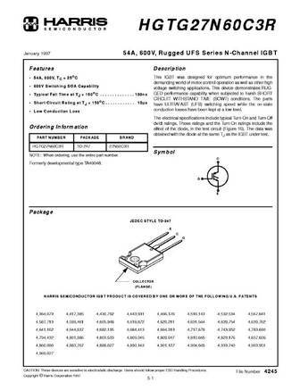
HGTG27N60C3DR TM Data Sheet June 2000 File Number 4262.1 54A, 600V, Rugged UFS Series N-Channel Features IGBT with Anti-Parallel Ultrafast Diode 54A, 600V, TC = 25oC [ /Title This IGBT was designed for optimum performance in the 600V Switching SOA Capability (HGT demanding world of motor control operation as well as other Typical Fall Time at TJ = 150oC . . . . . . . . .
mgp7n60erev0.pdf
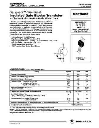
MOTOROLA Order this document SEMICONDUCTOR TECHNICAL DATA by MGP7N60E/D Designer's Data Sheet MGP7N60E Insulated Gate Bipolar Transistor N Channel Enhancement Mode Silicon Gate This Insulated Gate Bipolar Transistor (IGBT) uses an advanced IGBT IN TO 220 termination scheme to provide an enhanced and reliable high 9.0 A @ 90 C voltage blocking capability. Its new 600 V IG
mgp7n60e.pdf

MOTOROLA Order this document SEMICONDUCTOR TECHNICAL DATA by MGP7N60E/D Designer's Data Sheet MGP7N60E Insulated Gate Bipolar Transistor N Channel Enhancement Mode Silicon Gate This Insulated Gate Bipolar Transistor (IGBT) uses an advanced IGBT IN TO 220 termination scheme to provide an enhanced and reliable high 7.0 A @ 90 C voltage blocking capability. Its new 600 V IG
mgp7n60ed.pdf
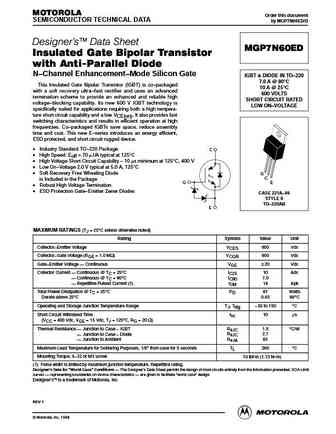
MOTOROLA Order this document SEMICONDUCTOR TECHNICAL DATA by MGP7N60ED/D Designer's Data Sheet MGP7N60ED Insulated Gate Bipolar Transistor with Anti-Parallel Diode N Channel Enhancement Mode Silicon Gate IGBT & DIODE IN TO 220 7.0 A @ 90 C This Insulated Gate Bipolar Transistor (IGBT) is co packaged 10 A @ 25 C with a soft recovery ultra fast rectifier and uses an ad
irfp27n60k.pdf
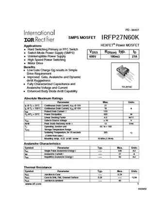
PD - 94407 SMPS MOSFET IRFP27N60K HEXFET Power MOSFET Applications Hard Switching Primary or PFC Switch VDSS RDS(on) typ. ID Switch Mode Power Supply (SMPS) Uninterruptible Power Supply 600V 180m 27A High Speed Power Switching Motor Drive Benefits Low Gate Charge Qg results in Simple Drive Requirement Improved Gate, Avalanche and Dynamic dv/dt Ruggedness Fully Char
irfp27n60kpbf.pdf
PD - 95479A SMPS MOSFET IRFP27N60KPbF HEXFET Power MOSFET Applications l Hard Switching Primary or PFC Switch VDSS RDS(on) typ. ID l Switch Mode Power Supply (SMPS) l Uninterruptible Power Supply 600V 180m 27A l High Speed Power Switching l Motor Drive l Lead-Free Benefits l Low Gate Charge Qg results in Simple Drive Requirement l Improved Gate, Avalanche and Dynamic dv/dt
irfb17n60k.pdf
PD - 95629 IRFB17N60KPbF Lead-Free 8/4/04 Document Number 91099 www.vishay.com 1 IRFB17N60KPbF Document Number 91099 www.vishay.com 2 IRFB17N60KPbF Document Number 91099 www.vishay.com 3 IRFB17N60KPbF Document Number 91099 www.vishay.com 4 IRFB17N60KPbF Document Number 91099 www.vishay.com 5 IRFB17N60KPbF Document Number 91099 www.vishay.com 6 IRFB17N60KPbF
phw7n60 1.pdf
Philips Semiconductors Product specification PowerMOS transistor PHW7N60 GENERAL DESCRIPTION QUICK REFERENCE DATA N-channel enhancement mode SYMBOL PARAMETER MAX. UNIT field-effect power transistor in a plastic envelope featuring high VDS Drain-source voltage 600 V avalanche energy capability, stable ID Drain current (DC) 7 A off-state characteristics, fast Ptot Total power dissipation
phw7n60.pdf
PHW7N60 Philips Semiconductors Product specification PowerMOS transistor PHW7N60 GENERAL DESCRIPTION QUICK REFERENCE DATA N-channel enhancement mode SYMBOL PARAMETER MAX. UNIT field-effect power transistor in a plastic envelope featuring high VDS Drain-source voltage 600 V avalanche energy capability, stable ID Drain current (DC) 7 A off-state characteristics, fast Ptot
phx7n60e.pdf
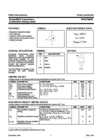
Philips Semiconductors Product specification PowerMOS transistors PHX7N60E Avalanche energy rated FEATURES SYMBOL QUICK REFERENCE DATA d Repetitive Avalanche Rated Fast switching VDSS = 600 V Stable off-state characteristics High thermal cycling performance ID = 3.6 A g Isolated package RDS(ON) 1.2 s GENERAL DESCRIPTION PINNING SOT186A N-channel, enh
php7n60e phb7n60e phw7n60e.pdf
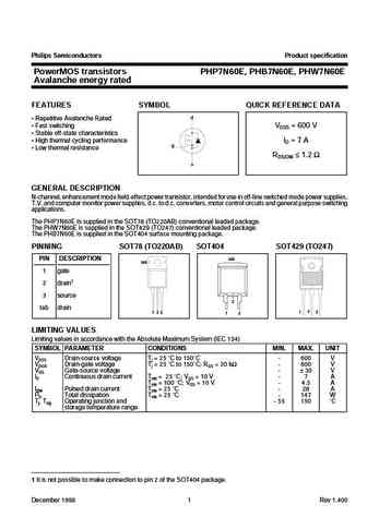
Philips Semiconductors Product specification PowerMOS transistors PHP7N60E, PHB7N60E, PHW7N60E Avalanche energy rated FEATURES SYMBOL QUICK REFERENCE DATA d Repetitive Avalanche Rated Fast switching VDSS = 600 V Stable off-state characteristics High thermal cycling performance ID = 7 A g Low thermal resistance RDS(ON) 1.2 s GENERAL DESCRIPTION N-chan
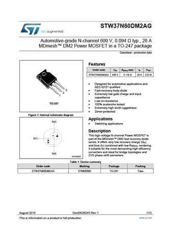
stb37n60dm2ag.pdf
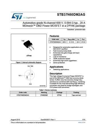
STB37N60DM2AG Automotive-grade N-channel 600 V, 0.094 typ., 28 A MDmesh DM2 Power MOSFET in a D PAK package Datasheet - production data Features Order code VDS RDS(on) max. ID PTOT TAB STB37N60DM2AG 600 V 0.110 28 A 210 W Designed for automotive applications and 3 AEC-Q101 qualified 1 Fast-recovery body diode Extremely low gate charge and input capa
stf7n60m2.pdf
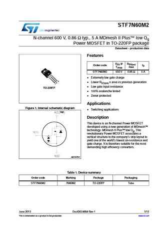
STF7N60M2 N-channel 600 V, 0.86 typ., 5 A MDmesh II Plus low Qg Power MOSFET in TO-220FP package Datasheet - production data Features VDS @ RDS(on) Order code ID TJmax max STF7N60M2 650 V 0.95 5 A Extremely low gate charge 3 2 Lower RDS(on) x area vs previous generation 1 Low gate input resistance TO-220FP 100% avalanche tested Zener-protected App
stw37n60dm2ag.pdf
STW37N60DM2AG Automotive-grade N-channel 600 V, 0.094 typ., 28 A MDmesh DM2 Power MOSFET in a TO-247 package Datasheet - production data Features Order code VDS RDS(on) max. ID PTOT STW37N60DM2AG 600 V 0.110 28 A 210 W Designed for automotive applications and AEC-Q101 qualified 3 Fast-recovery body diode 2 Extremely low gate charge and input 1 capac
stl7n60m2.pdf
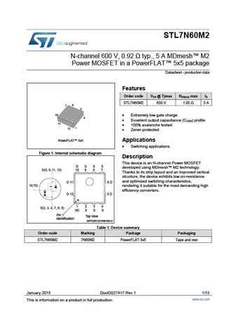
STL7N60M2 N-channel 600 V, 0.92 typ., 5 A MDmesh M2 Power MOSFET in a PowerFLAT 5x5 package Datasheet - production data Features Order code V @ Tjmax R max I DS DS(on) D STL7N60M2 650 V 1.05 5 A 6 7 5 Extremely low gate charge 4 Excellent output capacitance (COSS) profile 100% avalanche tested 1 12 Zener-protected PowerFLAT 5x5 Applic
std7n60m2 stp7n60m2 stu7n60m2.pdf
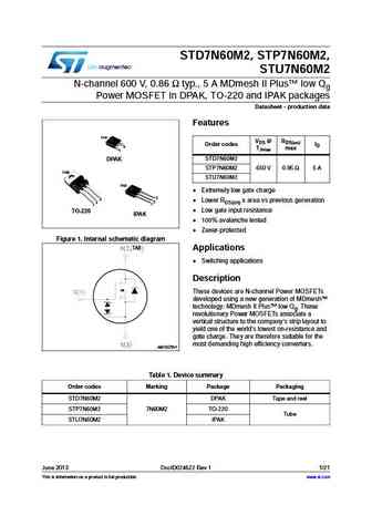
STD7N60M2, STP7N60M2, STU7N60M2 N-channel 600 V, 0.86 typ., 5 A MDmesh II Plus low Qg Power MOSFET in DPAK, TO-220 and IPAK packages Datasheet - production data Features TAB VDS @ RDS(on) Order codes ID 3 TJmax max 1 STD7N60M2 DPAK STP7N60M2 650 V 0.95 5 A TAB STU7N60M2 TAB Extremely low gate charge 3 3 2 Lower RDS(on) x area vs previous generation 2 1
hgtd7n60c3s hgtp7n60c3.pdf
HGTD7N60C3S, HGTP7N60C3 Data Sheet December 2001 14A, 600V, UFS Series N-Channel IGBTs Features The HGTD7N60C3S and HGTP7N60C3 are MOS gated 14A, 600V at TC = 25oC high voltage switching devices combining the best features 600V Switching SOA Capability of MOSFETs and bipolar transistors. These devices have the Typical Fall Time. . . . . . . . . . . . . . . . 140ns at TJ =
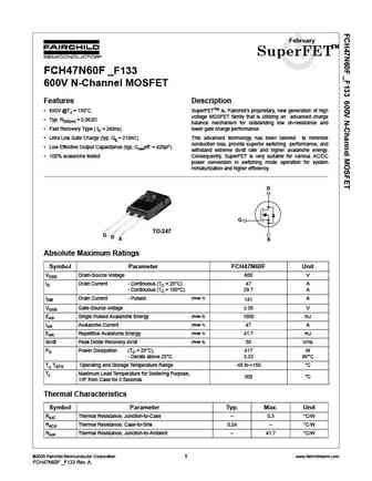
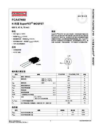
fch47n60 f133 fca47n60 fca47n60 f109.pdf
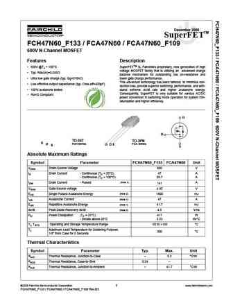
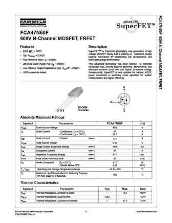
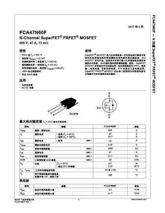
December 2008 TM SuperFET FCH47N60_F133 / FCA47N60 / FCA47N60_F109 600V N-Channel MOSFET Features Description 650V @TJ = 150 C SuperFETTM is, Fairchild s proprietary, new generation of high voltage MOSFET family that is utilizing an advanced charge Typ. Rds(on)=0.058 balance mechanism for outstanding low on-resistance and Ultra low gate charge (typ. Qg=210nC) lowe
hgt1s7n60c3ds hgtp7n60c3d.pdf
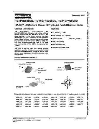
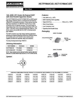
September 2005 HGTP7N60C3D, HGT1S7N60C3DS, HGT1S7N60C3D 14A, 600V, UFS Series N-Channel IGBT with Anti-Parallel Hyperfast Diodes General Description Features The HGTP7N60C3D, HGT1S7N60C3DS and 14A, 600V at TC = 25oC HGT1S7N60C3D are MOS gated high voltage switching devices combining the best features of MOSFETs and 600V Switching SOA Capability bipolar transistors. These devices ha
fcu7n60tu.pdf

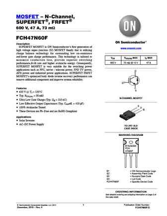
December 2008 TM SuperFET FCD7N60 / FCU7N60 600V N-Channel MOSFET Features Description 650V @TJ = 150 C SuperFETTM is, Fairchild s proprietary, new generation of high voltage MOSFET family that is utilizing an advanced charge Typ. Rds(on)=0.53 balance mechanism for outstanding low on-resistance and Ultra low gate charge (typ. Qg=23nC) lower gate charge performan
fch47n60f f085.pdf
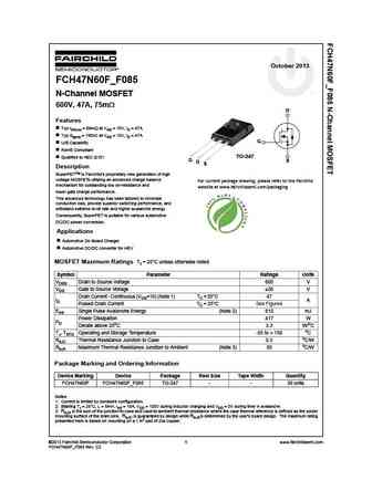
October 2013 FCH47N60F_F085 N-Channel MOSFET 600V, 47A, 75m D Features Typ rDS(on) = 66m at VGS = 10V, ID = 47A Typ Qg(tot) = 190nC at VGS = 10V, ID = 47A G UIS Capability RoHS Compliant TO-247 Qualified to AEC Q101 G S D S Description SuperFETTM is Fairchild s proprietary new generation of high voltage MOSFETs utilizing an advanced charge balance For curren
fch47n60 f085.pdf
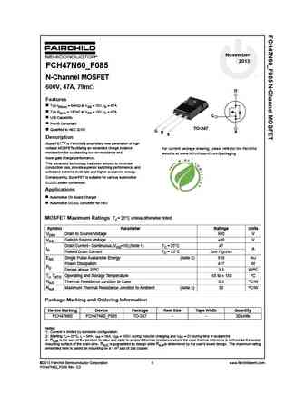
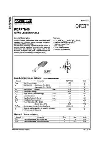
November 2013 FCH47N60_F085 N-Channel MOSFET 600V, 47A, 79m D Features Typ rDS(on) = 64m at VGS = 10V, ID = 47A Typ Qg(tot) = 187nC at VGS = 10V, ID = 47A G UIS Capability RoHS Compliant TO-247 Qualified to AEC Q101 G S D S Description SuperFETTM is Fairchild s proprietary new generation of high voltage MOSFETs utilizing an advanced charge balance For curren
ssp7n60b sss7n60b.pdf
SSP7N60B/SSS7N60B 600V N-Channel MOSFET General Description Features These N-Channel enhancement mode power field effect 7.0A, 600V, RDS(on) = 1.2 @VGS = 10 V transistors are produced using Fairchild s proprietary, Low gate charge ( typical 38 nC) planar, DMOS technology. Low Crss ( typical 23 pF) This advanced technology has been especially tailored to Fast switchi
fqp7n60.pdf
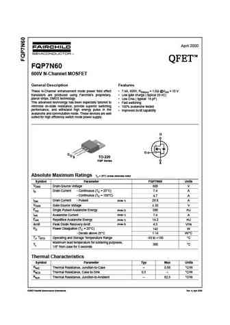
April 2000 TM QFET QFET QFET QFET FQP7N60 600V N-Channel MOSFET General Description Features These N-Channel enhancement mode power field effect 7.4A, 600V, RDS(on) = 1.0 @VGS = 10 V transistors are produced using Fairchild s proprietary, Low gate charge ( typical 29 nC) planar stripe, DMOS technology. Low Crss ( typical 16 pF) This advanced technology has been esp
hgtp7n60b3d hgt1s7n60b3d.pdf
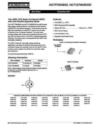
HGTP7N60B3D, HGT1S7N60B3DS Data Sheet December 2001 14A, 600V, UFS Series N-Channel IGBTs Features with Anti-Parallel Hyperfast Diode 14A, 600V, TC = 25oC The HGTP7N60B3D and HGT1S7N60B3DS are MOS gated 600V Switching SOA Capability high voltage switching devices combining the best features Typical Fall Time. . . . . . . . . . . . . . . . 120ns at TJ = 150oC of MOSFETs an
fch47n60n.pdf
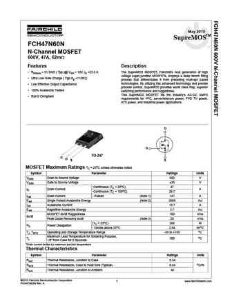
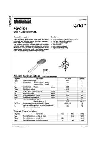
May 2010 SupreMOSTM FCH47N60N N-Channel MOSFET 600V, 47A, 62m Features Description RDS(on) = 51.5m ( Typ.)@ VGS = 10V, ID =23.5 A The SupreMOS MOSFET, Fairchild s next generation of high voltage super-junction MOSFETs, employs a deep trench filling Ultra Low Gate Charge ( Typ.Qg =115nC) process that differentiates it from preceding multi-epi based technologies. By ut
fch47n60nf.pdf

January 2011 SupreMOSTM FCH47N60NF N-Channel MOSFET, FRFET 600V, 47A, 65m Features Description RDS(on) = 57.5m (Typ.) @ VGS = 10V, ID = 23.5A The SupreMOS MOSFET, Fairchild s next generation of high voltage super-junction MOSFETs, employs a deep trench filling Ultra Low Gate Charge (Typ. Qg = 121nC) process that differentiates it from preceding multi-epi based techno
fcp7n60 fcpf7n60 fcpf7n60ydtu fcpf7n60t fcpf7n60ydtu.pdf
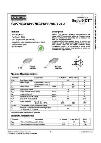
December 2008 TM SuperFET FCP7N60/FCPF7N60/FCPF7N60YDTU Features Description 650V @TJ = 150 C SuperFETTM is, Fairchild s proprietary, new generation of high voltage MOSFET family that is utilizing an advanced charge Typ. Rds(on)=0.53 balance mechanism for outstanding low on-resistance and Ultra low gate charge (typ. Qg=25nC) lower gate charge performance. This advan
fch47n60f.pdf
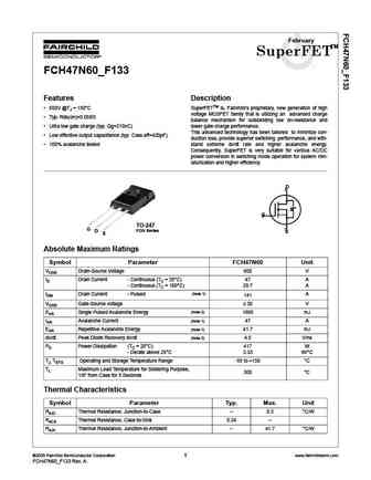
February TM SuperFET FCH47N60F _F133 600V N-Channel MOSFET Features Description 650V @TJ = 150 C SuperFETTM is, Fairchild s proprietary, new generation of high voltage MOSFET family that is utilizing an advanced charge Typ. RDS(on) = 0.062 balance mechanism for outstanding low on-resistance and Fast Recovery Type ( trr = 240ns) lower gate charge performance. Ult
fci7n60.pdf
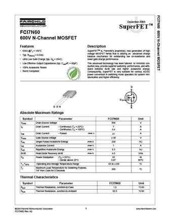
December 2008 TM SuperFET FCI7N60 600V N-Channel MOSFET Features Description 650V @TJ = 150 C SuperFETTM is, Fairchild s proprietary, new generation of high voltage MOSFET family that is utilizing an advanced charge Typ. RDS(on) = 0.53 balance mechanism for outstanding low on-resistance and Ultra Low Gate Charge (typ. Qg = 25nC) lower gate charge performance.
fdd7n60nz fdd7n60nztm fdu7n60nztu.pdf
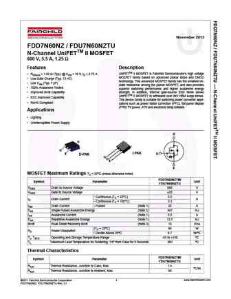
November 2013 FDD7N60NZ / FDU7N60NZTU N-Channel UniFETTM II MOSFET 600 V, 5.5 A, 1.25 Features Description RDS(on) = 1.05 (Typ.) @ VGS = 10 V, ID = 2.75 A UniFETTM II MOSFET is Fairchild Semiconductor s high voltage MOSFET family based on advanced planar stripe and DMOS Low Gate Charge (Typ. 13 nC) technology. This advanced MOSFET family has the smallest on- Low Crs
fca47n60f.pdf
January 2009 TM SuperFET FCA47N60F 600V N-Channel MOSFET, FRFET Features Description 650V @TJ = 150 C SuperFETTM is, Fairchild s proprietary, new generation of high voltage MOSFET family that is utilizing an advanced charge Typ. RDS(on) = 0.062 balance mechanism for outstanding low on-resistance and Fast Recovery Type ( trr = 240ns) lower gate charge performance.
fqa7n60.pdf
April 2000 TM QFET QFET QFET QFET FQA7N60 600V N-Channel MOSFET General Description Features These N-Channel enhancement mode power field effect 7.7A, 600V, RDS(on) = 1.0 @VGS = 10 V transistors are produced using Fairchild s proprietary, Low gate charge ( typical 29 nC) planar stripe, DMOS technology. Low Crss ( typical 16 pF) This advanced technology has been esp
fch47n60 fch47n60 f133.pdf
February TM SuperFET FCH47N60_F133 Features Description 650V @TJ = 150 C SuperFETTM is, Fairchild s proprietary, new generation of high voltage MOSFET family that is utilizing an advanced charge Typ. Rds(on)=0.058 balance mechanism for outstanding low on-resistance and Ultra low gate charge (typ. Qg=210nC) lower gate charge performance. This advanced technology has
fqpf7n60.pdf
April 2000 TM QFET QFET QFET QFET FQPF7N60 600V N-Channel MOSFET General Description Features These N-Channel enhancement mode power field effect 4.3A, 600V, RDS(on) = 1.0 @VGS = 10 V transistors are produced using Fairchild s proprietary, Low gate charge ( typical 29 nC) planar stripe, DMOS technology. Low Crss ( typical 16 pF) This advanced technology has been es
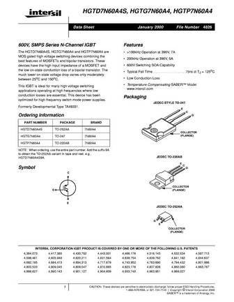
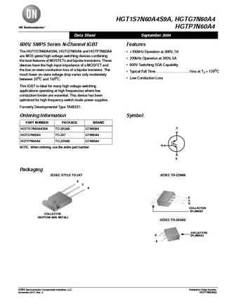
hgtp7n60a4 hgtg7n60a4 hgt1s7n60a4.pdf
HGT1S7N60A4S9A, HGTG7N60A4 HGTP7N60A4 Data Sheet September 2004 600V, SMPS Series N-Channel IGBT Features The HGT1S7N60A4S9A, HGTG7N60A4 and HGTP7N60A4 >100kHz Operation at 390V, 7A are MOS gated high voltage switching devices combining 200kHz Operation at 390V, 5A the best features of MOSFETs and bipolar transistors. These 600V Switching SOA Capability devices have t
fdp7n60nz fdpf7n60nz.pdf
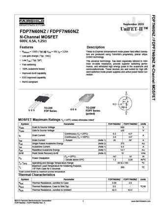
September 2010 UniFET-II TM FDP7N60NZ / FDPF7N60NZ N-Channel MOSFET 600V, 6.5A, 1.25 Features Description RDS(on) = 1.05 ( Typ.)@ VGS = 10V, ID = 3.25A These N-Channel enhancement mode power field effect transis- tors are produced using Fairchild s proprietary, planar stripe, Low gate charge ( Typ. 13nC) DOMS technology. Low Crss ( Typ. 7pF) This advance techn
fcp7n60n fcpf7n60nt.pdf
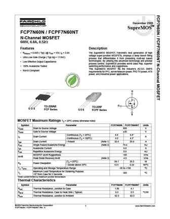
December 2009 SupreMOSTM FCP7N60N / FCPF7N60NT N-Channel MOSFET 600V, 6.8A, 0.52 Features Description RDS(on) = 0.46 ( Typ.) @ VGS = 10V, ID = 3.4A The SupreMOS MOSFET, Fairchild s next generation of high voltage super-junction MOSFETs, employs a deep trench filling Ultra Low Gate Charge ( Typ.Qg = 17.8nC) process that differentiates it from preceding multi-epi based
fqb7n60tm fqb7n60 fqi7n60 fqi7n60tu.pdf
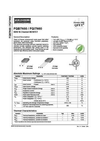
October 2008 QFET FQB7N60 / FQI7N60 600V N-Channel MOSFET General Description Features These N-Channel enhancement mode power field effect 7.4A, 600V, RDS(on) = 1.0 @VGS = 10 V transistors are produced using Fairchild s proprietary, Low gate charge ( typical 29 nC) planar stripe, DMOS technology. Low Crss ( typical 16 pF) This advanced technology has been especially
fdp17n60n fdpf17n60nt.pdf
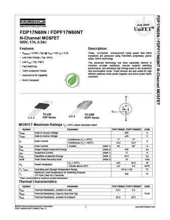
July 2009 UniFETTM FDP17N60N / FDPF17N60NT N-Channel MOSFET 600V, 17A, 0.34 Features Description RDS(on) = 0.29 ( Typ.)@ VGS = 10V, ID = 8.5A These N-Channel enhancement mode power field effect transistors are produced using Fairchild s proprietary, planar Low Gate Charge ( Typ. 48nC) stripe, DMOS technology. Low Crss ( Typ. 23pF) This advanced technology has b
fcd7n60 fcu7n60.pdf
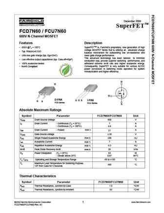
December 2008 TM SuperFET FCD7N60 / FCU7N60 600V N-Channel MOSFET Features Description 650V @TJ = 150 C SuperFETTM is, Fairchild s proprietary, new generation of high voltage MOSFET family that is utilizing an advanced charge Typ. Rds(on)=0.53 balance mechanism for outstanding low on-resistance and Ultra low gate charge (typ. Qg=23nC) lower gate charge performan
ssw7n60a.pdf
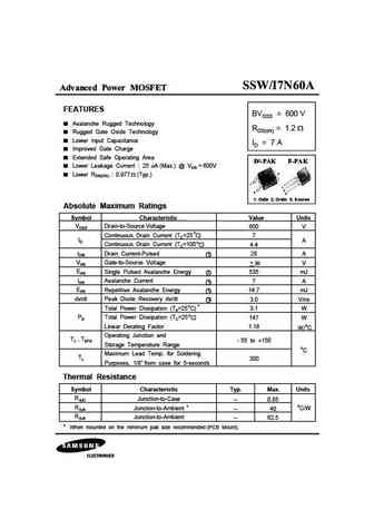
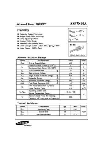
Advanced Power MOSFET FEATURES BVDSS = 600 V Avalanche Rugged Technology RDS(on) = 1.2 Rugged Gate Oxide Technology Lower Input Capacitance ID = 7 A Improved Gate Charge Extended Safe Operating Area Lower Leakage Current 25 A (Max.) @ VDS = 600V 2 Lower RDS(ON) 0.977 (Typ.) 1 1 2 3 3 1. Gate 2. Drain 3. Source Absolute Maximum Ratings Symbol Chara
ssh7n60a.pdf

Advanced Power MOSFET FEATURES BVDSS = 600 V Avalanche Rugged Technology RDS(on) = 1.2 Rugged Gate Oxide Technology Lower Input Capacitance ID = 7.3 A Improved Gate Charge Extended Safe Operating Area Lower Leakage Current 25 A (Max.) @ VDS = 600V Lower RDS(ON) 0.977 (Typ.) 1 2 3 1.Gate 2. Drain 3. Source Absolute Maximum Ratings Symbol Characteristic Va
ssp7n60a.pdf
Advanced Power MOSFET FEATURES BVDSS = 600 V Avalanche Rugged Technology RDS(on) = 1.2 Rugged Gate Oxide Technology Lower Input Capacitance ID = 7 A Improved Gate Charge Extended Safe Operating Area Lower Leakage Current 25 A (Max.) @ VDS = 600V Lower RDS(ON) 0.977 (Typ.) 1 2 3 1.Gate 2. Drain 3. Source Absolute Maximum Ratings Symbol Characteristic Valu
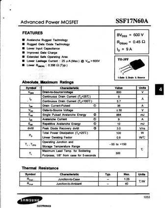
ssh17n60a.pdf
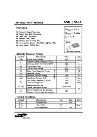
Advanced Power MOSFET FEATURES BVDSS = 600 V Avalanche Rugged Technology RDS(on) = 0.45 Rugged Gate Oxide Technology Lower Input Capacitance ID = 17 A Improved Gate Charge Extended Safe Operating Area Lower Leakage Current 25 A (Max.) @ VDS = 600V Lower RDS(ON) 0.356 (Typ.) 1 2 3 1.Gate 2. Drain 3. Source Absolute Maximum Ratings Symbol Characteristic Va
sss7n60a.pdf
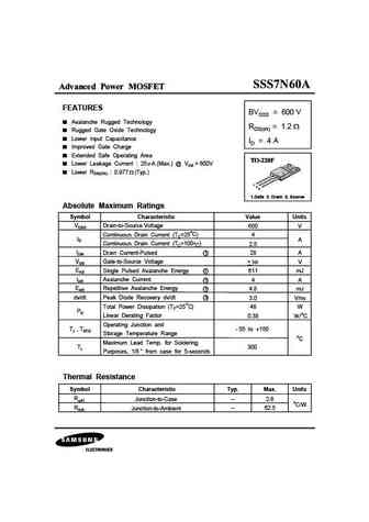
Advanced Power MOSFET FEATURES BVDSS = 600 V Avalanche Rugged Technology RDS(on) = 1.2 Rugged Gate Oxide Technology Lower Input Capacitance ID = 4 A Improved Gate Charge Extended Safe Operating Area Lower Leakage Current 25 A (Max.) @ VDS = 600V Lower RDS(ON) 0.977 (Typ.) 1 2 3 1.Gate 2. Drain 3. Source Absolute Maximum Ratings Symbol Characteristic Valu
irfp27n60k sihfp27n60k.pdf
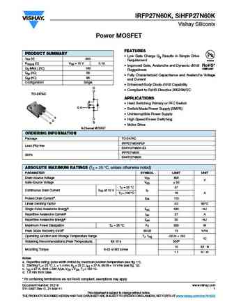
IRFP27N60K, SiHFP27N60K Vishay Siliconix Power MOSFET FEATURES PRODUCT SUMMARY Low Gate Charge Qg Results in Simple Drive VDS (V) 600 Available Requirement RDS(on) ( )VGS = 10 V 0.18 RoHS* Improved Gate, Avalanche and Dynamic dV/dt Qg (Max.) (nC) 180 COMPLIANT Ruggedness Qgs (nC) 56 Fully Characterized Capacitance and Avalanche Voltage Qgd (nC) 86 and Current Co
sihp17n60d.pdf
SiHP17N60D www.vishay.com Vishay Siliconix D Series Power MOSFET FEATURES PRODUCT SUMMARY Optimal Design VDS (V) at TJ max. 650 - Low Area Specific On-Resistance RDS(on) max. at 25 C ( ) VGS = 10 V 0.340 - Low Input Capacitance (Ciss) Qg (Max.) (nC) 90 - Reduced Capacitive Switching Losses Qgs (nC) 14 - High Body Diode Ruggedness Qgd (nC) 22 - Avalanche Energy Rated (UIS
sihg17n60d.pdf
SiHG17N60D www.vishay.com Vishay Siliconix D Series Power MOSFET FEATURES PRODUCT SUMMARY Optimal Design VDS (V) at TJ max. 650 - Low Area Specific On-Resistance RDS(on) max. at 25 C ( ) VGS = 10 V 0.340 - Low Input Capacitance (Ciss) Qg (Max.) (nC) 90 - Reduced Capacitive Switching Losses Qgs (nC) 14 - High Body Diode Ruggedness Qgd (nC) 22 - Avalanche Energy Rated (UIS
irfb17n60k irfb17n60kpbf.pdf
IRFB17N60K, SiHFB17N60K Vishay Siliconix Power MOSFET FEATURES PRODUCT SUMMARY Smaller TO-220 Package VDS (V) 600 Available Low Gate Charge Qg Results in Simple Drive RDS(on) ( )VGS = 10 V 0.35 RoHS* Requirement Qg (Max.) (nC) 99 COMPLIANT Improved Gate, Avalanche and Dynamic dV/dt Qgs (nC) 32 Ruggedness Qgd (nC) 47 Fully Characterized Capacitance and Avalanc
sihg47n60s.pdf
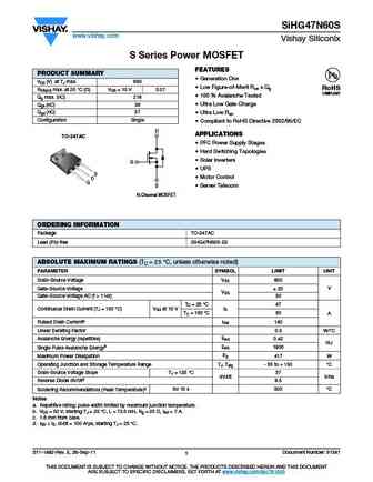
SiHG47N60S www.vishay.com Vishay Siliconix S Series Power MOSFET FEATURES PRODUCT SUMMARY Generation One VDS (V) at TJ max. 650 Low Figure-of-Merit Ron x Qg RoHS RDS(on) max. at 25 C ( ) VGS = 10 V 0.07 COMPLIANT 100 % Avalanche Tested Qg max. (nC) 216 Ultra Low Gate Charge Qgs (nC) 39 Qgd (nC) 57 Ultra Low Ron Configuration Single Compliant to R
sihp7n60e.pdf
SiHP7N60E www.vishay.com Vishay Siliconix E Series Power MOSFET FEATURES PRODUCT SUMMARY Low Figure-of-Merit (FOM) Ron x Qg VDS (V) at TJ max. 650 Low Input Capacitance (Ciss) RDS(on) max. at 25 C ( ) VGS = 10 V 0.6 Reduced Switching and Conduction Losses Qg max. (nC) 40 Ultra Low Gate Charge (Qg) Qgs (nC) 5 Avalanche Energy Rated (UIS) Qgd (nC) 9 Mate
sihd7n60e.pdf
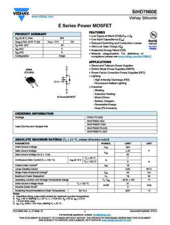
SiHD7N60E www.vishay.com Vishay Siliconix E Series Power MOSFET FEATURES PRODUCT SUMMARY Low Figure-of-Merit (FOM) Ron x Qg VDS (V) at TJ max. 650 Low Input Capacitance (Ciss) RDS(on) max. at 25 C ( ) VGS = 10 V 0.6 Reduced Switching and Conduction Losses Qg max. (nC) 40 Ultra Low Gate Charge (Qg) Qgs (nC) 5 Avalanche Energy Rated (UIS) Qgd (nC) 9 Mate
sihg47n60ef.pdf
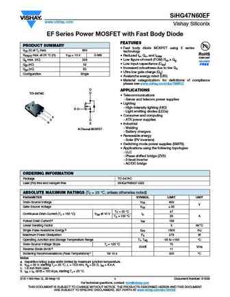
SiHG47N60EF www.vishay.com Vishay Siliconix EF Series Power MOSFET with Fast Body Diode FEATURES PRODUCT SUMMARY Fast body diode MOSFET using E series VDS (V) at TJ max. 650 technology RDS(on) max. at 25 C ( ) VGS = 10 V 0.065 Reduced trr, Qrr, and IRRM Qg max. (nC) 228 Low figure-of-merit (FOM) Ron x Qg Low input capacitance (Ciss) Qgs (nC) 32 Increased r
sihh27n60ef.pdf
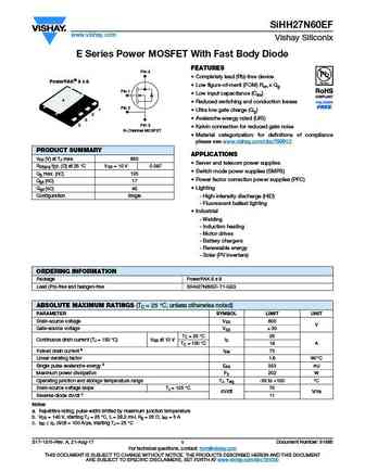
SiHH27N60EF www.vishay.com Vishay Siliconix E Series Power MOSFET With Fast Body Diode FEATURES Pin 4 Completely lead (Pb)-free device PowerPAK 8 x 8 Low figure-of-merit (FOM) Ron x Qg Pin 1 Low input capacitance (Ciss) 4 Reduced switching and conduction losses Pin 2 1 Ultra low gate charge (Qg) 2 Avalanche energy rated (UIS) 3 3 Pin 3 Kelvin co
irfp27n60k irfp27n60kpbf sihfp27n60k.pdf

IRFP27N60K, SiHFP27N60K Vishay Siliconix Power MOSFET FEATURES PRODUCT SUMMARY Low Gate Charge Qg Results in Simple Drive VDS (V) 600 Available Requirement RDS(on) ( )VGS = 10 V 0.18 RoHS* Improved Gate, Avalanche and Dynamic dV/dt Qg (Max.) (nC) 180 COMPLIANT Ruggedness Qgs (nC) 56 Fully Characterized Capacitance and Avalanche Voltage Qgd (nC) 86 and Current Co
sihu7n60e.pdf
SiHU7N60E www.vishay.com Vishay Siliconix E Series Power MOSFET FEATURES PRODUCT SUMMARY Low Figure-of-Merit (FOM) Ron x Qg VDS (V) at TJ max. 650 Low Input Capacitance (Ciss) RDS(on) max. at 25 C ( ) VGS = 10 V 0.6 Reduced Switching and Conduction Losses Qg max. (nC) 40 Ultra Low Gate Charge (Qg) Qgs (nC) 5 Avalanche Energy Rated (UIS) Qgd (nC) 9 Mate
sihg47n60aef.pdf
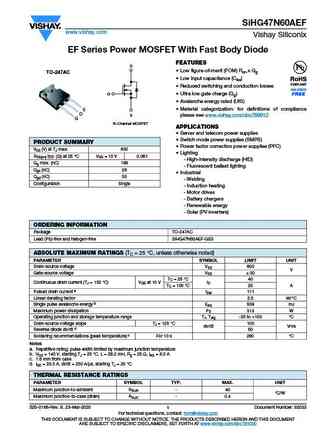
SiHG47N60AEF www.vishay.com Vishay Siliconix EF Series Power MOSFET With Fast Body Diode FEATURES D Low figure-of-merit (FOM) Ron x Qg TO-247AC Low input capacitance (Ciss) Reduced switching and conduction losses G Ultra low gate charge (Qg) Avalanche energy rated (UIS) Material categorization for definitions of compliance S D S please see www.vishay.com
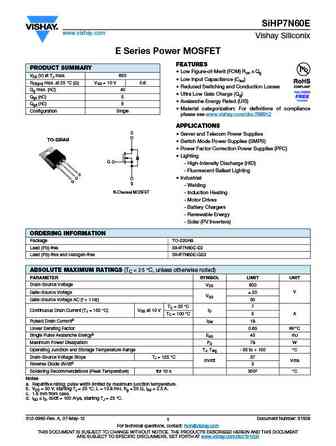
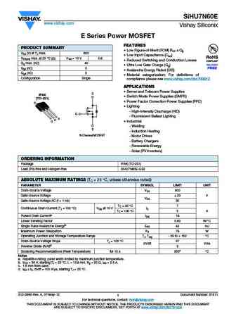
sihg47n60e.pdf
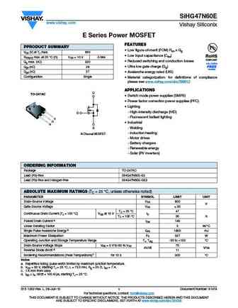
SiHG47N60E www.vishay.com Vishay Siliconix E Series Power MOSFET FEATURES PPRODUCT SUMMARY Low figure-of-merit (FOM) Ron x Qg VDS (V) at TJ max. 650 Low input capacitance (Ciss) RDS(on) max. at 25 C ( ) VGS = 10 V 0.064 Reduced switching and conduction losses Qg max. (nC) 220 Ultra low gate charge (Qg) Qgs (nC) 29 Available Qgd (nC) 57 Avalanche energy ra
sihf7n60e.pdf
SiHF7N60E www.vishay.com Vishay Siliconix E Series Power MOSFET FEATURES PRODUCT SUMMARY Low Figure-of-Merit (FOM) Ron x Qg VDS (V) at TJ max. 650 Low Input Capacitance (Ciss) RDS(on) max. at 25 C ( ) VGS = 10 V 0.6 Reduced Switching and Conduction Losses Qg max. (nC) 40 Ultra Low Gate Charge (Qg) Qgs (nC) 5 Avalanche Energy Rated (UIS) Qgd (nC) 9 Mate
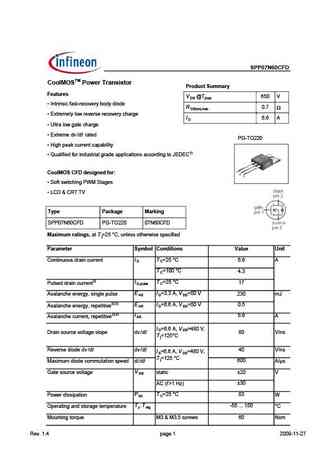
spb07n60c3.pdf
SPB07N60C3 Cool MOS Power Transistor VDS @ Tjmax 650 V Feature RDS(on) 0.6 New revolutionary high voltage technology ID 7.3 A Ultra low gate charge PG-TO263 Periodic avalanche rated Extreme dv/dt rated High peak current capability Improved transconductance Type Package Ordering Code Marking SPB07N60C3 PG-TO263 Q67040-S4394 07N60C3 Maximum Ratings P
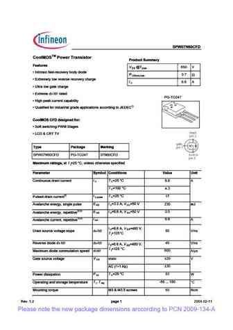
spw47n60cfd.pdf
SPW47N60CFD TM C IMOSTM "9@/; %;+877+;B Features V - R (7H C7GA>FE;A@3CJ ;9 GA>E397 E75 @A>A9J DS(on) max R $@EC;@D;5 83DE C75AG7CJ 4A6J 6;A67 46 A 46 D R IEC7?7>J >AH C7G7CD7 C75AG7CJ 5 3C97 R / >EC3 >AH 93E7 5 3C97 PG TO247 R IEC7?7 6v /dt C3E76 /d R #;9 B73= 5FCC7@E 53B34;>;EJ R *7C;A6;5 3G3>3@5 7 C3E76 R + F3>;8;76 355AC6;@9 EA % R *4 8C77
spd07n60s5 spu07n60s5.pdf
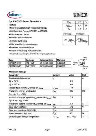
SPU07N60S5 SPD07N60S5 Cool MOS Power Transistor VDS 600 V Feature RDS(on) 0.6 New revolutionary high voltage technology ID 7.3 A Worldwide best RDS(on) in TO-251 and TO-252 PG-TO252 PG-TO251 Ultra low gate charge Periodic avalanche rated 2 3 Extreme dv/dt rated 3 1 2 1 Ultra low effective capacitances Improved transconductance Type Packag
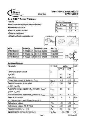
spp07n60c3 spi07n60c3 spa07n60c3.pdf
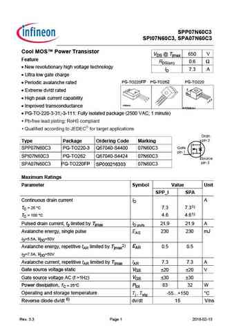
SPP07N60C3 SPI07N60C3, SPA07N60C3 Cool MOS Power Transistor VDS @ Tjmax 650 V Feature RDS(on) 0.6 New revolutionary high voltage technology ID 7.3 A Ultra low gate charge PG-TO220FP PG-TO262 PG-TO220 Periodic avalanche rated 2 Extreme dv/dt rated 3 High peak current capability 2 3 2 1 1 P-TO220-3-31 Improved transconductance P-TO220-3-1 P
spp07n60c3 spa07n60c3 spi07n60c3 rev.3.2.pdf
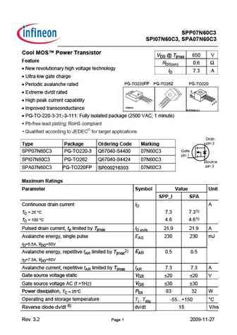
SPP07N60C3 SPI07N60C3, SPA07N60C3 Cool MOS Power Transistor VDS @ Tjmax 650 V Feature RDS(on) 0.6 New revolutionary high voltage technology ID 7.3 A Ultra low gate charge PG-TO220FP PG-TO262 PG-TO220 Periodic avalanche rated 2 Extreme dv/dt rated 3 High peak current capability 2 3 2 1 1 P-TO220-3-31 Improved transconductance P-TO220-3-1 P
spw07n60cfd.pdf
SPW07N60CFD TM C IMOSTM # A0D9 R 0.7 DS(on) max V "MIG B AN ADL G K GH G 8DK GN 8=6G;> 9 688DG9>CC
spb07n60s5.pdf
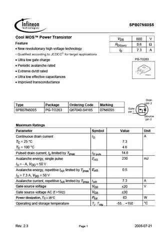
SPB07N60S5 Cool MOS Power Transistor VDS 600 V Feature RDS(on) 0.6 New revolutionary high voltage technology ID 7.3 A PG-TO263 Ultra low gate charge Periodic avalanche rated Extreme dv/dt rated Ultra low effective capacitances Improved transconductance Type Package Ordering Code Marking 07N60S5 SPB07N60S5 PG-TO263 Q67040-S4185 Maximum Ratings Par
spa07n60cfd.pdf
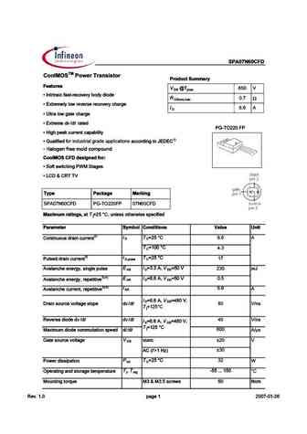
SPA07N60CFD C IMOSTM $;B1= '=- >5>?;= $=;0@/? &@99-=D Features V 1jmax 650 V DS V &CIG>CH>8 ;6HI G 8DK GN 7D9N 9>D9 R 0.7 DS(on) max V "MIG B AN ADL G K GH G 8DK GN 8=6G;> 9 for industrial grade applications 688DG9>C53 10 2;= V 0D;I HL>I8=>C
spa07n60c2 spp07n60c2 spb07n60c2.pdf
SPP07N60C2, SPB07N60C2 Final data SPA07N60C2 Cool MOS Power Transistor Feature Product Summary New revolutionary high voltage technology VDS @ Tjmax 650 V Ultra low gate charge RDS(on) 0.6 Periodic avalanche rated ID 7.3 A Extreme dv/dt rated Ultra low effective capacitances P-TO220-3-31 P-TO263-3-2 P-TO220-3-1 3 2 1 P-TO220-3-31 Type Package Orderi
spp07n60s5 spi07n60s5.pdf
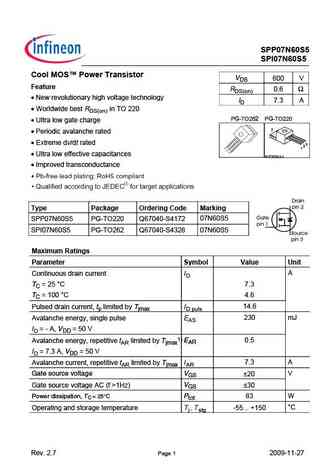
SPP07N60S5 SPI07N60S5 Cool MOS Power Transistor VDS 600 V Feature RDS(on) 0.6 New revolutionary high voltage technology ID 7.3 A Worldwide best RDS(on) in TO 220 PG-TO262 PG-TO220 Ultra low gate charge 2 Periodic avalanche rated Extreme dv/dt rated 3 2 1 Ultra low effective capacitances P-TO220-3-1 Improved transconductance Type Package Or
ixgp7n60bd1.pdf
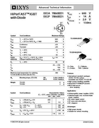
Advanced Technical Information IXGA 7N60BD1 VCES = 600 V HiPerFASTTM IGBT IXGP 7N60BD1 IC25 = 14 A with Diode VCE(sat) = 2.0 V tfi = 150ns Symbol Test Conditions Maximum Ratings TO-220AB (IXGP) VCES TJ = 25 C to 150 C 600 V VCGR TJ = 25 C to 150 C; RGE = 1 M 600 V VGES Continuous 20 V G C E VGEM Transient 30 V IC25 TC = 25 C 14 A TO-263 AA (IXGA) IC90 TC = 90 C 7
ixfa7n60p3 ixfp7n60p3.pdf
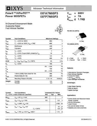
Advance Technical Information Polar3 TM HiPerFETTM VDSS = 600V IXFA7N60P3 Power MOSFETs ID25 = 7A IXFP7N60P3 RDS(on) 1.15 N-Channel Enhancement Mode Avalanche Rated Fast Intrinsic Rectifier TO-263 AA (IXFA) G Symbol Test Conditions Maximum Ratings S VDSS TJ = 25 C to 150 C 600 V D (Tab) VDGR TJ = 25 C to 150 C, RGS = 1M 600 V TO-220AB
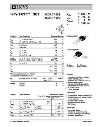
ixga7n60c.pdf

VCES = 600 V IXGA 7N60C HiPerFASTTM IGBT IC25 = 14 A IXGP 7N60C LightspeedTM Series VCE(sat) = 2.7 V tfi = 45 ns Symbol Test Conditions Maximum Ratings TO-220AB (IXGP) VCES TJ = 25 C to 150 C 600 V VCGR TJ = 25 C to 150 C; RGE = 1 M 600 V G C E VGES Continuous 20 V VGEM Transient 30 V TO-263 AA (IXGA) IC25 TC = 25 C 14 A IC90 TC = 90 C 7 A ICM TC = 25 C, 1 ms 30
ixgp7n60cd1.pdf

IXGA 7N60CD1 VCES = 600 V HiPerFASTTM IGBT IXGP 7N60CD1 IC25 = 14 A with Diode VCE(sat)typ = 2.0 V LightspeedTM Series tfi = 45 ns Preliminary Data Symbol Test Conditions Maximum Ratings TO-220AB (IXGP) VCES TJ = 25 C to 150 C 600 V VCGR TJ = 25 C to 150 C; RGE = 1 M 600 V VGES Continuous 20 V G C E VGEM Transient 30 V IC25 TC = 25 C 14 A TO-263 AA (IXGA) IC90 TC
ixga7n60c ixgp7n60c.pdf

VCES = 600 V IXGA 7N60C HiPerFASTTM IGBT IC25 = 14 A IXGP 7N60C LightspeedTM Series VCE(sat) = 2.7 V tfi = 45 ns Symbol Test Conditions Maximum Ratings TO-220AB (IXGP) VCES TJ = 25 C to 150 C 600 V VCGR TJ = 25 C to 150 C; RGE = 1 M 600 V G C E VGES Continuous 20 V VGEM Transient 30 V TO-263 AA (IXGA) IC25 TC = 25 C 14 A IC90 TC = 90 C 7 A ICM TC = 25 C, 1 ms 30
ixta7n60p ixtp7n60p.pdf
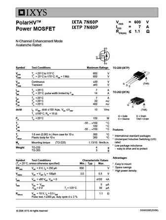
VDSS = 600 V IXTA 7N60P PolarHVTM ID25 = 7 A IXTP 7N60P Power MOSFET RDS(on) 1.1 N-Channel Enhancement Mode Avalanche Rated Symbol Test Conditions Maximum Ratings TO-220 (IXTP) VDSS TJ = 25 C to 175 C 600 V VDGR TJ = 25 C to 175 C; RGS = 1 M 600 V VGS Continuous 30 V (TAB) G VGSM Transient 40 V D S ID25 TC = 25 C7 A
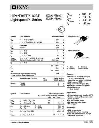
ixga7n60b.pdf

VCES = 600 V HiPerFASTTM IGBT IXGA 7N60B IC25 = 14 A IXGP 7N60B VCE(sat) = 2 V tfi = 150 ns Symbol Test Conditions Maximum Ratings TO-220AB (IXGP) VCES TJ = 25 C to 150 C 600 V VCGR TJ = 25 C to 150 C; RGE = 1 M 600 V G C E VGES Continuous 20 V VGEM Transient 30 V TO-263 AA (IXGA) IC25 TC = 25 C 14 A IC90 TC = 90 C 7 A ICM TC = 25 C, 1 ms 30 A G C (TAB) E SSOA
ixga7n60b ixgp7n60b.pdf

VCES = 600 V HiPerFASTTM IGBT IXGA 7N60B IC25 = 14 A IXGP 7N60B VCE(sat) = 2 V tfi = 150 ns Symbol Test Conditions Maximum Ratings TO-220AB (IXGP) VCES TJ = 25 C to 150 C 600 V VCGR TJ = 25 C to 150 C; RGE = 1 M 600 V G C E VGES Continuous 20 V VGEM Transient 30 V TO-263 AA (IXGA) IC25 TC = 25 C 14 A IC90 TC = 90 C 7 A ICM TC = 25 C, 1 ms 30 A G C (TAB) E SSOA
ixgp7n60c.pdf
VCES = 600 V IXGA 7N60C HiPerFASTTM IGBT IC25 = 14 A IXGP 7N60C LightspeedTM Series VCE(sat) = 2.7 V tfi = 45 ns Symbol Test Conditions Maximum Ratings TO-220AB (IXGP) VCES TJ = 25 C to 150 C 600 V VCGR TJ = 25 C to 150 C; RGE = 1 M 600 V G C E VGES Continuous 20 V VGEM Transient 30 V TO-263 AA (IXGA) IC25 TC = 25 C 14 A IC90 TC = 90 C 7 A ICM TC = 25 C, 1 ms 30
ixga7n60bd1.pdf

Advanced Technical Information IXGA 7N60BD1 VCES = 600 V HiPerFASTTM IGBT IXGP 7N60BD1 IC25 = 14 A with Diode VCE(sat) = 2.0 V tfi = 150ns Symbol Test Conditions Maximum Ratings TO-220AB (IXGP) VCES TJ = 25 C to 150 C 600 V VCGR TJ = 25 C to 150 C; RGE = 1 M 600 V VGES Continuous 20 V G C E VGEM Transient 30 V IC25 TC = 25 C 14 A TO-263 AA (IXGA) IC90 TC = 90 C 7
ixga7n60cd1.pdf
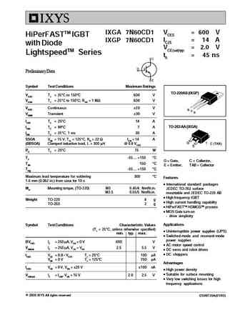
IXGA 7N60CD1 VCES = 600 V HiPerFASTTM IGBT IXGP 7N60CD1 IC25 = 14 A with Diode VCE(sat)typ = 2.0 V LightspeedTM Series tfi = 45 ns Preliminary Data Symbol Test Conditions Maximum Ratings TO-220AB (IXGP) VCES TJ = 25 C to 150 C 600 V VCGR TJ = 25 C to 150 C; RGE = 1 M 600 V VGES Continuous 20 V G C E VGEM Transient 30 V IC25 TC = 25 C 14 A TO-263 AA (IXGA) IC90 TC
ixgp7n60b.pdf
VCES = 600 V HiPerFASTTM IGBT IXGA 7N60B IC25 = 14 A IXGP 7N60B VCE(sat) = 2 V tfi = 150 ns Symbol Test Conditions Maximum Ratings TO-220AB (IXGP) VCES TJ = 25 C to 150 C 600 V VCGR TJ = 25 C to 150 C; RGE = 1 M 600 V G C E VGES Continuous 20 V VGEM Transient 30 V TO-263 AA (IXGA) IC25 TC = 25 C 14 A IC90 TC = 90 C 7 A ICM TC = 25 C, 1 ms 30 A G C (TAB) E SSOA
hgt1s7n60a4s9a hgtg7n60a4 hgtp7n60a4.pdf
HGT1S7N60A4S9A, HGTG7N60A4 HGTP7N60A4 Data Sheet September 2004 600V, SMPS Series N-Channel IGBT Features The HGT1S7N60A4S9A, HGTG7N60A4 and HGTP7N60A4 >100kHz Operation at 390V, 7A are MOS gated high voltage switching devices combining 200kHz Operation at 390V, 5A the best features of MOSFETs and bipolar transistors. These 600V Switching SOA Capability devices have t
hgtd7n60c3s hgtp7n60c3.pdf

Is Now Part of To learn more about ON Semiconductor, please visit our website at www.onsemi.com Please note As part of the Fairchild Semiconductor integration, some of the Fairchild orderable part numbers will need to change in order to meet ON Semiconductor s system requirements. Since the ON Semiconductor product management systems do not have the ability to manage part nomenclatur
fgb7n60undf.pdf

Is Now Part of To learn more about ON Semiconductor, please visit our website at www.onsemi.com Please note As part of the Fairchild Semiconductor integration, some of the Fairchild orderable part numbers will need to change in order to meet ON Semiconductor s system requirements. Since the ON Semiconductor product management systems do not have the ability to manage part nomenclatur
fcd7n60.pdf

Is Now Part of To learn more about ON Semiconductor, please visit our website at www.onsemi.com Please note As part of the Fairchild Semiconductor integration, some of the Fairchild orderable part numbers will need to change in order to meet ON Semiconductor s system requirements. Since the ON Semiconductor product management systems do not have the ability to manage part nomenclatur
fch47n60n.pdf

Is Now Part of To learn more about ON Semiconductor, please visit our website at www.onsemi.com Please note As part of the Fairchild Semiconductor integration, some of the Fairchild orderable part numbers will need to change in order to meet ON Semiconductor s system requirements. Since the ON Semiconductor product management systems do not have the ability to manage part nomenclatur
fcpf7n60nt.pdf

Is Now Part of To learn more about ON Semiconductor, please visit our website at www.onsemi.com Please note As part of the Fairchild Semiconductor integration, some of the Fairchild orderable part numbers will need to change in order to meet ON Semiconductor s system requirements. Since the ON Semiconductor product management systems do not have the ability to manage part nomenclatur
fch47n60nf.pdf

Is Now Part of To learn more about ON Semiconductor, please visit our website at www.onsemi.com Please note As part of the Fairchild Semiconductor integration, some of the Fairchild orderable part numbers will need to change in order to meet ON Semiconductor s system requirements. Since the ON Semiconductor product management systems do not have the ability to manage part nomenclatur
fcp7n60 fcpf7n60.pdf

Is Now Part of To learn more about ON Semiconductor, please visit our website at www.onsemi.com Please note As part of the Fairchild Semiconductor integration, some of the Fairchild orderable part numbers will need to change in order to meet ON Semiconductor s system requirements. Since the ON Semiconductor product management systems do not have the ability to manage part nomenclatur
fch47n60f.pdf
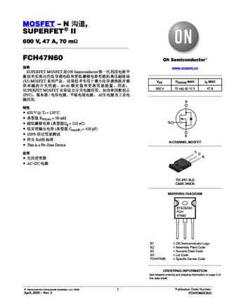
MOSFET N-Channel, SUPERFET), FRFET) 600 V, 47 A, 73 mW FCH47N60F Description SUPERFET MOSFET is ON Semiconductor s first generation of www.onsemi.com high voltage super-junction (SJ) MOSFET family that is utilizing charge balance technology for outstanding low on-resistance and lower gate charge performance. This technology is tailored to VDS RDS(ON) MAX ID MAX minimize conduct
fci7n60.pdf

Is Now Part of To learn more about ON Semiconductor, please visit our website at www.onsemi.com Please note As part of the Fairchild Semiconductor integration, some of the Fairchild orderable part numbers will need to change in order to meet ON Semiconductor s system requirements. Since the ON Semiconductor product management systems do not have the ability to manage part nomenclatur
fdp7n60nz fdpf7n60nz.pdf

Is Now Part of To learn more about ON Semiconductor, please visit our website at www.onsemi.com Please note As part of the Fairchild Semiconductor integration, some of the Fairchild orderable part numbers will need to change in order to meet ON Semiconductor s system requirements. Since the ON Semiconductor product management systems do not have the ability to manage part nomenclatur
fqb7n60 fqi7n60.pdf
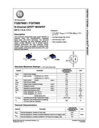
FQB7N60 / FQI7N60 N-Channel QFET MOSFET 600 V, 7.4 A, 1.0 Features 7.4 A, 600 V, RDS(on) = 1.0 (Max.) @VGS = 10 V, Description ID = 3.7 A This N-Channel enhancement mode power MOSFET is Low Gate Charge (Typ. 29 nC) produced using ON Semiconductor s proprietary Low Crss (Typ. 16 pF) planar stripe and DMOS technology. This advanced MOSFET technology has been
hgtg7n60a4d hgtp7n60a4d hgt1s7n60a4ds.pdf
SMPS Series N-Channel IGBT with Anti-Parallel Hyperfast Diode 600 V HGTG7N60A4D, www.onsemi.com HGTP7N60A4D, HGT1S7N60A4DS The HGTG7N60A4D, HGTP7N60A4D and HGT1S7N60A4DS are MOS gated high voltage switching devices combining the best features of MOSFETs and bipolar transistors. These devices have the high input impedance of a MOSFET and the low on-state conduction loss of a bipolar
7n60l.pdf
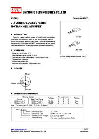
UNISONIC TECHNOLOGIES CO., LTD 7N60L Power MOSFET 7.4 Amps, 600/650 Volts N-CHANNEL MOSFET DESCRIPTION The UTC 7N60L is a high voltage MOSFET and is designed to have better characteristics, such as fast switching time, low gate charge, low on-state resistance and have a high rugged avalanche characteristics. This power MOSFET is usually used at high speed switching applicati
7n60a.pdf
UNISONIC TECHNOLOGIES CO., LTD 7N60A Power MOSFET 7A, 600V N-CHANNEL POWER MOSFET DESCRIPTION The UTC 7N60A is a high voltage N-Channel enhancement mode power field effect transistors and is designed to have minimize on-state resistance , provide superior switching performance, and withstand high energy pulse in the avalanche and commutation mode. This power MOSFET is well sui
7n60l-ta3-t 7n60g-ta3-t 7n60l-tf3-t 7n60g-tf3-t 7n60l-tf1-t 7n60g-tf1-t 7n60l-tf2-t 7n60g-tf2-t.pdf

UNISONIC TECHNOLOGIES CO., LTD 7N60 Power MOSFET 7.4A, 600V N-CHANNEL POWER MOSFET DESCRIPTION The UTC 7N60 is a high voltage power MOSFET and is designed to have better characteristics, such as fast switching time, low gate charge, low on-state resistance and have a high rugged avalanche characteristics. This power MOSFET is usually used at high speed switching applicatio
7n60k.pdf

UNISONIC TECHNOLOGIES CO., LTD 7N60K Power MOSFET 7.4A, 600V N-CHANNEL POWER MOSFET DESCRIPTION The UTC 7N60K is a high voltage power MOSFET and is designed to have better characteristics, such as fast switching time, low gate charge, low on-state resistance and have a high rugged avalanche characteristics. This power MOSFET is usually used at high speed switching applicat
7n60l-tf3t-t 7n60g-tf3t-t 7n60l-t2q-t 7n60g-t2q-t 7n60l-tq2-t 7n60g-tq2-t 7n60l-tq2-r 7n60g-tq2-r.pdf
UNISONIC TECHNOLOGIES CO., LTD 7N60 Power MOSFET 7.4A, 600V N-CHANNEL POWER MOSFET DESCRIPTION The UTC 7N60 is a high voltage power MOSFET and is designed to have better characteristics, such as fast switching time, low gate charge, low on-state resistance and have a high rugged avalanche characteristics. This power MOSFET is usually used at high speed switching applicatio
7n60z.pdf
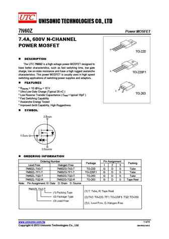
UNISONIC TECHNOLOGIES CO., LTD 7N60Z Power MOSFET 7.4A, 600V N-CHANNEL POWER MOSFET 1 TO-220 DESCRIPTION The UTC 7N60Z is a high voltage power MOSFET designed to have better characteristics, such as fast switching time, low gate charge, low on-state resistance and have a high rugged avalanche 1 TO-220F1 characteristics. This power MOSFET is usually used in high speed swi
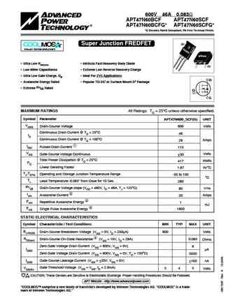
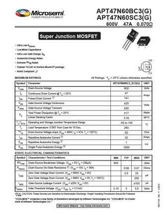
apt47n60bc3.pdf
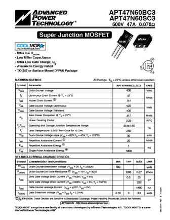
APT47N60BC3 APT47N60SC3 600V 47A 0.070 Super Junction MOSFET D3PAK TO-247 COOLMOS Power Semiconductors Ultra low RDS(ON) Low Miller Capacitance D Ultra Low Gate Charge, Qg Avalanche Energy Rated G TO-247 or Surface Mount D3PAK Package S MAXIMUM RATINGS All Ratings TC = 25 C unless otherwise specified. Symbol Parameter APT47N60BC3_SC3
apt47n60bcfg.pdf
FINAL DATA SHEET 600V 46A 0.083 APT47N60BCF APT47N60SCF APT47N60BCFG* APT47N60SCFG* *G Denotes RoHS Compliant, Pb Free Terminal Finish. Super Junction FREDFET (B) COOLMOS Power Semiconductors D3PAK Ultra Low RDS(ON) Intrinsic Fast-Recovery Body Diode (S) Low Miller Capacitance Extreme Low Reverse Recovery Charge Ultra Low Gate Charge, Qg Ideal For Z
apt77n60jc3.pdf
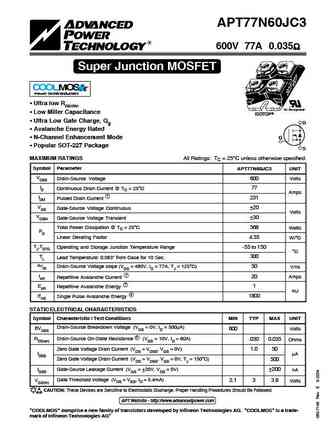
APT77N60JC3 600V 77A 0.035 Super Junction MOSFET COOLMOS Power Semiconductors Ultra low RDS(ON) "UL Recognized" Low Miller Capacitance ISOTOP Ultra Low Gate Charge, Qg D Avalanche Energy Rated N-Channel Enhancement Mode G Popular SOT-227 Package S MAXIMUM RATINGS All Ratings TC = 25 C unless otherwise specified. Symbol Parameter
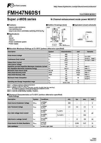
fmh17n60es.pdf
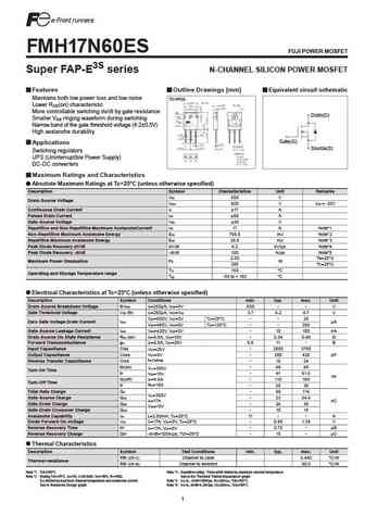
FMH17N60ES FUJI POWER MOSFET Super FAP-E3S series N-CHANNEL SILICON POWER MOSFET Features Outline Drawings [mm] Equivalent circuit schematic Maintains both low power loss and low noise TO-3P(Q) Lower R (on) characteristic DS More controllable switching dv/dt by gate resistance Drain(D) Smaller V ringing waveform during switching GS Narrow band of the gate threshold voltage (4.2 0.5V
fmw47n60s1hf.pdf
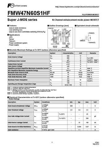
http //www.fujielectric.com/products/semiconductor/ FMW47N60S1HF FUJI POWER MOSFET Super J-MOS series N-Channel enhancement mode power MOSFET Features Outline Drawings [mm] Equivalent circuit schematic Low on-state resistance TO-247-P2 Low switching loss easy to use (more controllabe switching dV/dt by R ) g Drain(D) Applications UPS Server Gate(G) Telecom Source(S)
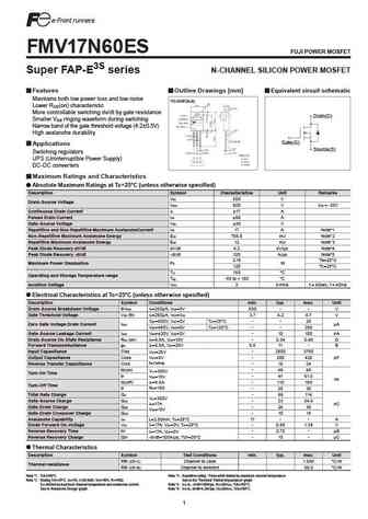
fmh47n60s1.pdf
http //www.fujielectric.com/products/semiconductor/ FMH47N60S1 FUJI POWER MOSFET Super J-MOS series N-Channel enhancement mode power MOSFET Features Outline Drawings [mm] Equivalent circuit schematic Low on-state resistance 3.2 0.1 TO-3P 15.5max 13 0.2 1.5 0.2 Low switching loss 10 0.2 4.5 0.2 easy to use (more controllabe switching dV/dt by R ) g Drain(D) Applications
fmr17n60es.pdf

FMR17N60ES FUJI POWER MOSFET Super FAP-E3S series N-CHANNEL SILICON POWER MOSFET Features Outline Drawings [mm] Equivalent circuit schematic Maintains both low power loss and low noise TO-3PF Lower R (on) characteristic DS More controllable switching dv/dt by gate resistance Drain(D) Smaller V ringing waveform during switching GS Narrow band of the gate threshold voltage (4.2 0.5V)
fmv17n60es.pdf
FMV17N60ES FUJI POWER MOSFET Super FAP-E3S series N-CHANNEL SILICON POWER MOSFET Features Outline Drawings [mm] Equivalent circuit schematic Maintains both low power loss and low noise TO-220F(SLS) Lower R (on) characteristic DS More controllable switching dv/dt by gate resistance Drain(D) Smaller V ringing waveform during switching GS Narrow band of the gate threshold voltage (4.2
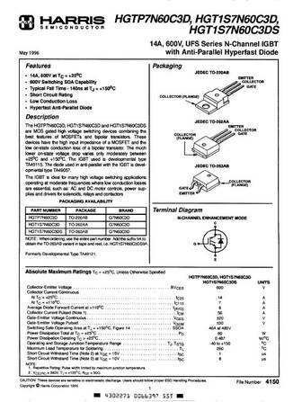
hgtp7n60.pdf
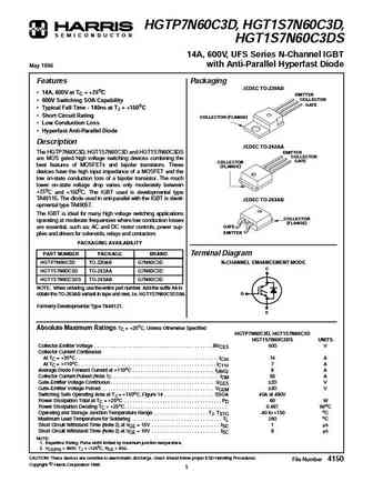
HGTP7N60C3D, HGT1S7N60C3D, S E M I C O N D U C T O R HGT1S7N60C3DS 14A, 600V, UFS Series N-Channel IGBT with Anti-Parallel Hyperfast Diode May 1996 Features Packaging JEDEC TO-220AB 14A, 600V at TC = +25oC EMITTER COLLECTOR 600V Switching SOA Capability GATE Typical Fall Time - 140ns at TJ = +150oC Short Circuit Rating COLLECTOR (FLANGE) Low Conduction Loss
hgtd7n60.pdf
HGTD7N60C3, S E M I C O N D U C T O R HGTD7N60C3S, HGTP7N60C3 14A, 600V, UFS Series N-Channel IGBT June 1996 Features Packaging JEDEC TO-220AB 14A, 600V at TC = +25oC COLLECTOR EMITTER 600V Switching SOA Capability GATE Typical Fall Time - 140ns at TJ = +150oC Short Circuit Rating Low Conduction Loss COLLECTOR (FLANGE) Description JEDEC TO-251AA The HGTD7N60C
tsm7n60ci tsm7n60cz.pdf
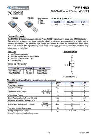
TSM7N60 600V N-Channel Power MOSFET ITO-220 TO-220 Pin Definition PRODUCT SUMMARY 1. Gate 2. Drain VDS (V) RDS(on)( ) ID (A) 3. Source 600 1.2 @ VGS =10V 3.5 General Description The TSM7N60 N-Channel enhancement mode Power MOSFET is produced by planar stripe DMOS technology. This advanced technology has been especially tailored to minimize on-state resistance, provide su
cjp07n60.pdf
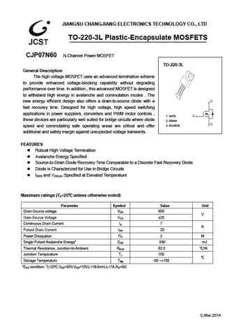
JIANGSU CHANGJIANG ELECTRONICS TECHNOLOGY CO., LTD TO-220-3L Plastic-Encapsulate MOSFETS CJP07N60 N-Channel Power MOSFET TO-220-3L General Description The high voltage MOSFET uses an advanced termination scheme to provide enhanced voltage-blocking capability without degrading performance over time. In addition , this advanced MOSFET is designed to withstand high energy in ava
cjpf07n60.pdf
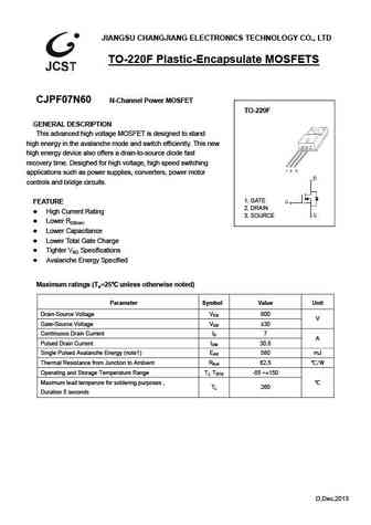
JIANGSU CHANGJIANG ELECTRONICS TECHNOLOGY CO., LTD TO-220F Plastic-Encapsulate MOSFETS CJPF07N60 N-Channel Power MOSFET TO-220F GENERAL DESCRIPTION This advanced high voltage MOSFET is designed to stand high energy in the avalanche mode and switch efficiently. This new high energy device also offers a drain-to-source diode fast recovery time. Desighed for high voltage, high s
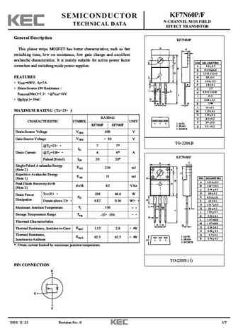
kf7n60p kf7n60f.pdf
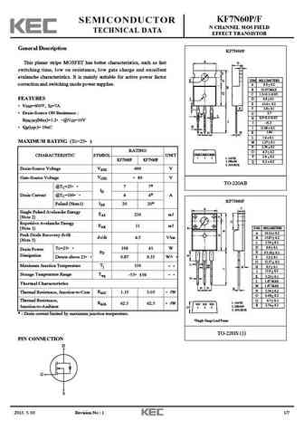
KF7N60P/F SEMICONDUCTOR N CHANNEL MOS FIELD TECHNICAL DATA EFFECT TRANSISTOR General Description KF7N60P A This planar stripe MOSFET has better characteristics, such as fast O C switching time, low on resistance, low gate charge and excellent F avalanche characteristics. It is mainly suitable for active power factor E DIM MILLIMETERS G _ correction and switching mode power supp
kf7n60p-f.pdf
KF7N60P/F SEMICONDUCTOR N CHANNEL MOS FIELD TECHNICAL DATA EFFECT TRANSISTOR General Description KF7N60P A This planar stripe MOSFET has better characteristics, such as fast O C switching time, low on resistance, low gate charge and excellent F avalanche characteristics. It is mainly suitable for active power factor E DIM MILLIMETERS G _ correction and switching mode power supp
apt47n60bc3g apt47n60sc3g.pdf
APT47N60BC3(G) APT47N60SC3(G) 600V 47A 0.070 Super Junction MOSFET D3PAK Ultra Low RDS(ON) Low Miller Capacitance Ultra Low Gate Charge, Qg Avalanche Energy Rated D Extreme dv/dt Rated Popular TO-247 or Surface Mount D3 package. G RoHS Compliant S MAXIMUM RATINGS All Ratings TC = 25 C unless otherwise specified. Symbol Parameter APT47N60B
apt77n60bc6 apt77n60sc6.pdf
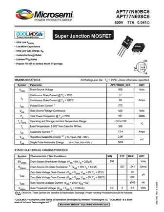
APT77N60BC6 APT77N60SC6 600V 77A 0.041 COOLMOS Power Semiconductors Super Junction MOSFET Ultra Low RDS(ON) D3PAK Low Miller Capacitance Ultra Low Gate Charge, Qg Avalanche Energy Rated Extreme dv/dt Rated D Popular TO-247 or Surface Mount D3 package. G S MAXIMUM RATINGS All Ratings per die TC = 25 C unless otherwise specified. Symbol Parame
wnm07n60-f.pdf
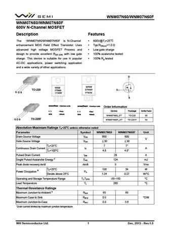
WNM07N60/WNM07N60F WNM07N60/WNM07N60F 600V N-Channel MOSFET Description Features C The WNM07N60/WNM07N60F is N-Channel 600V@TJ=25 enhancement MOS Field Effect Transistor. Uses Typ.RDS(on)=1.0 advanced high voltage MOSFET Process and Low gate charge design to provide excellent RDS (ON) with low gate 100% avalanche tested charge. This device is suitable for use in p
h07n60.pdf
Spec. No. MOS200604 HI-SINCERITY Issued Date 2006.02.01 Revised Date 2006.02.07 MICROELECTRONICS CORP. Page No. 1/5 H07N60 Series Pin Assignment H07N60 Series Tab N-Channel Power Field Effect Transistor 3-Lead Plastic TO-220AB Package Code E Pin 1 Gate Pin 2 & Tab Drain Description Pin 3 Source This high voltage MOSFET uses an advanced termination schem
aotf7n60.pdf

AOT7N60/AOTF7N60 600V,7A N-Channel MOSFET General Description Product Summary VDS 700V@150 The AOT7N60 & AOTF7N60 have been fabricated using an advanced high voltage MOSFET process that is ID (at VGS=10V) 7A designed to deliver high levels of performance and RDS(ON) (at VGS=10V)
aotf7n60fd.pdf
AOTF7N60FD 600V, 7A N-Channel MOSFET with Fast Recovery Diode General Description Product Summary VDS 700V@150 The AOTF7N60FD has been fabricated using an advanced high voltage MOSFET process that is designed ID (at VGS=10V) 7A to deliver high levels of performance and robustness in RDS(ON) (at VGS=10V)
aot7n60.pdf
AOT7N60/AOTF7N60 600V,7A N-Channel MOSFET General Description Product Summary VDS 700V@150 The AOT7N60 & AOTF7N60 have been fabricated using an advanced high voltage MOSFET process that is ID (at VGS=10V) 7A designed to deliver high levels of performance and RDS(ON) (at VGS=10V)
aoi7n60.pdf

AOD7N60/AOI7N60 600V,7A N-Channel MOSFET General Description Product Summary The AOD7N60 & AOI7N60 have been fabricated using an advanced high voltage MOSFET process that is designed VDS 700V@150 to deliver high levels of performance and robustness in ID (at VGS=10V) 7A popular AC-DC applications. RDS(ON) (at VGS=10V)
aod7n60 aoi7n60.pdf

AOD7N60/AOI7N60 600V,7A N-Channel MOSFET General Description Product Summary The AOD7N60 & AOI7N60 have been fabricated using an advanced high voltage MOSFET process that is designed VDS 700V@150 to deliver high levels of performance and robustness in ID (at VGS=10V) 7A popular AC-DC applications. RDS(ON) (at VGS=10V)
aot7n60 aotf7n60.pdf
AOT7N60/AOTF7N60 600V,7A N-Channel MOSFET General Description Product Summary VDS 700V@150 The AOT7N60 & AOTF7N60 have been fabricated using an advanced high voltage MOSFET process that is ID (at VGS=10V) 7A designed to deliver high levels of performance and RDS(ON) (at VGS=10V)
aod7n60.pdf
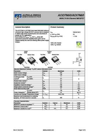
AOD7N60/AOI7N60 600V,7A N-Channel MOSFET General Description Product Summary The AOD7N60 & AOI7N60 have been fabricated using an advanced high voltage MOSFET process that is designed VDS 700V@150 to deliver high levels of performance and robustness in ID (at VGS=10V) 7A popular AC-DC applications. RDS(ON) (at VGS=10V)
ftp07n60 fta07n60.pdf
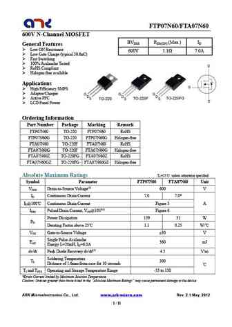
FTP07N60/FT A07N60 600V N-Channel MOSFET BVDSS RDS(ON) (Max.) ID General Features Low ON Resistance 600V 1.1 7.0A Low Gate Charge (typical 38.6nC) Fast Switching 100% Avalanche Tested RoHS Compliant Halogen-free available Applications High Efficiency SMPS Adaptor/Charger Active PFC LCD Panel Power Ordering Information
sss7n60.pdf
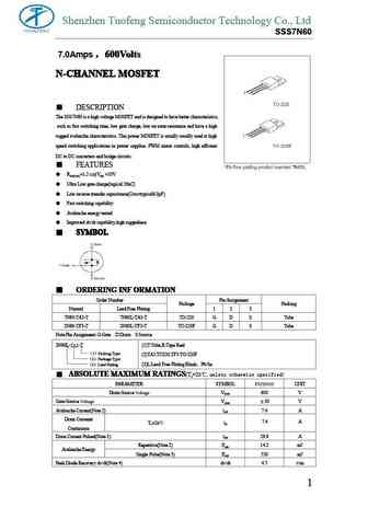
Shenzhen Tuofeng Semiconductor Technology Co., Ltd SSS7N60 600Volts 7.0Amps 600Volts 600Volts 600Volts N-CHANNEL MOSFET N-CHANNEL MOSFET N-CHANNEL MOSFET N-CHANNEL MOSFET DESCRIPTION The SSS7N60 is a high voltage MOSFET and is designed to have better characteristics, such as fast switching time, low gate charge, low on-state resistance and have a high rugged avalanche chara
sif7n60d.pdf
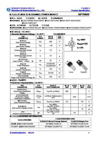
Shenzhen SI Semiconductors Co., LTD. Product Specification Shenzhen SI Semiconductors Co., LTD. Product Specification Shenzhen SI Semiconductors Co., LTD. Product Specification Shenzhen SI Semiconductors Co., LTD. Product Specification N- MOS / N-CHANNEL POWER MOSFET SIF7N60D N- MOS / N-CHANNEL POWER MOSFET SIF7N60D N
sif7n60c.pdf
Shenzhen SI Semiconductors Co., LTD. Product Specification Shenzhen SI Semiconductors Co., LTD. Product Specification Shenzhen SI Semiconductors Co., LTD. Product Specification Shenzhen SI Semiconductors Co., LTD. Product Specification N- MOS / N-CHANNEL POWER MOSFET SIF7N60C N- MOS / N-CHANNEL POWER MOSFET SIF7N60C N
jcs7n60bb jcs7n60sb jcs7n60cb jcs7n60fb.pdf
N R N-CHANNEL MOSFET JCS7N60B MAIN CHARACTERISTICS Package ID 7.0 A VDSS 600 V Rdson-max 1.2 @Vgs=10V Qg-typ 25 nC APPLICATIONS High efficiency switch mode power supplies Electronic lamp ballasts LED based on half bridge L
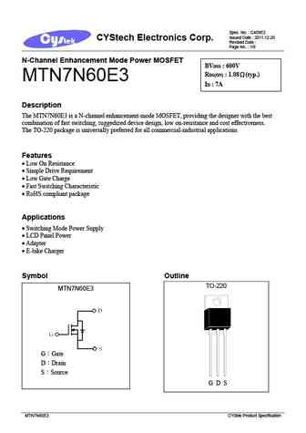
mtn7n60e3.pdf
Spec. No. C409E3 Issued Date 2011.12.20 CYStech Electronics Corp. Revised Date Page No. 1/9 N-Channel Enhancement Mode Power MOSFET BVDSS 600V RDS(ON) 1.08 (typ.) MTN7N60E3 ID 7A Description The MTN7N60E3 is a N-channel enhancement-mode MOSFET, providing the designer with the best combination of fast switching, ruggedized device design, low on-resistance an
mtn7n60fp.pdf
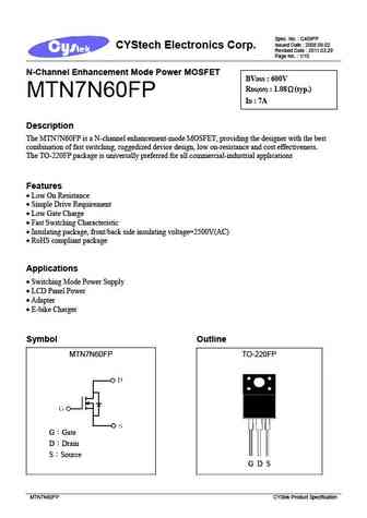
Spec. No. C409FP Issued Date 2008.09.02 CYStech Electronics Corp. Revised Date 2011.03.29 Page No. 1/10 N-Channel Enhancement Mode Power MOSFET BVDSS 600V RDS(ON) 1.08 (typ.) MTN7N60FP ID 7A Description The MTN7N60FP is a N-channel enhancement-mode MOSFET, providing the designer with the best combination of fast switching, ruggedized device design, low on-r
ssf7n60.pdf
SSF7N60 Features VDSS = 600V Extremely high dv/dt capability ID = 7A Low Gate Charge Qg results in Simple Drive Requirement Rdson = 0.9 (typ.) 100% avalanche tested Gate charge minimized Very low intrinsic capacitances Very good manufacturing repeatability Description The SSF7N60 is a new generation of high voltage N Channel enhancement mode
ssf7n60f.pdf
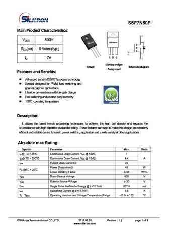
SSF7N60F Main Product Characteristics VDSS 600V RDS(on) 0.9ohm(typ.) ID 7A Marking and p in TO220F Schematic diagram Assignment Features and Benefits Advanced trench MOSFET process technology Special designed for PWM, load switching and general purpose applications Ultra low on-resistance with low gate charge Fast switching and reverse body recovery
fsa07n60a.pdf
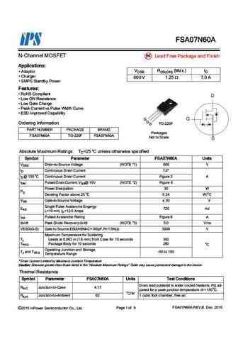
FSA07N60A N-Channel MOSFET Pb Lead Free Package and Finish Applications VDSS RDS(ON) (Max.) ID Adaptor Charger 600 V 1.25 7.0 A SMPS Standby Power Features RoHS Compliant Low ON Resistance Low Gate Charge Peak Current vs Pulse Width Curve ESD improved Capability G DS TO-220F Ordering Information PART NUMBER PACKAGE BRAND Packages FSA07N6
brb7n60.pdf
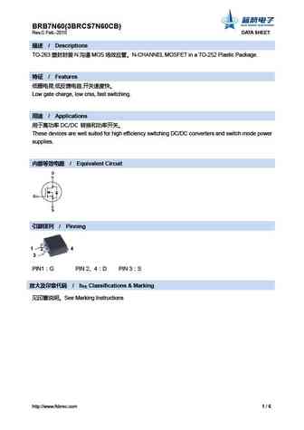
BRB7N60(3BRCS7N60CB) Rev.C Feb.-2015 DATA SHEET / Descriptions TO-263 N MOS N-CHANNEL MOSFET in a TO-252 Plastic Package. / Features , , Low gate charge, low crss, fast switching. / Applications DC/DC These devices are well suited for hi
brf7n60.pdf
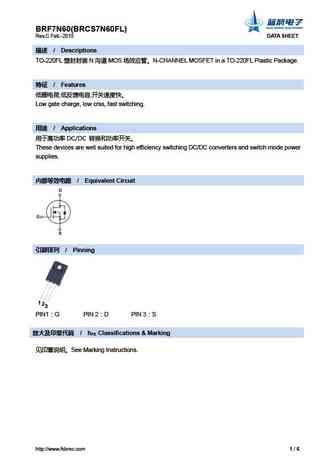
BRF7N60(BRCS7N60FL) Rev.C Feb.-2015 DATA SHEET / Descriptions TO-220FL N MOS N-CHANNEL MOSFET in a TO-220FL Plastic Package. / Features , , Low gate charge, low crss, fast switching. / Applications DC/DC These devices are well suited for
brd7n60.pdf
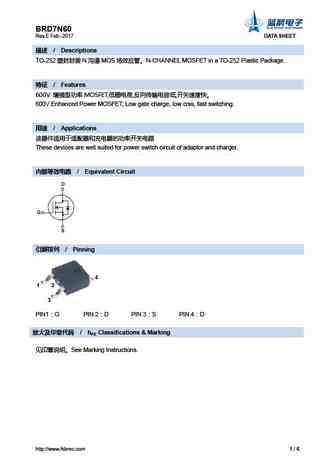
BRD7N60 Rev.E Feb.-2017 DATA SHEET / Descriptions TO-252 N MOS N-CHANNEL MOSFET in a TO-252 Plastic Package. / Features 600V MOSFET, , , 600V Enhanced Power MOSFET, Low gate charge, low crss, fast switching. / Applications
bri7n60.pdf
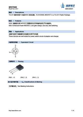
BRI7N60 Rev.B Feb.-2017 DATA SHEET / Descriptions TO-251 N MOS N-CHANNEL MOSFET in a TO-251 Plastic Package. / Features 600V MOSFET, , , 600V Enhanced Power MOSFET, Low gate charge, low crss, fast switching. / Applications
brfl7n60.pdf
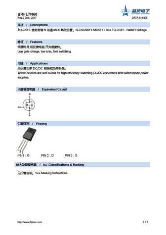
BRFL7N60 Rev.E Dec.-2017 DATA SHEET / Descriptions TO-220FL N MOS N-CHANNEL MOSFET in a TO-220FL Plastic Package. / Features , , Low gate charge, low crss, fast switching. / Applications DC/DC These devices are well suited for high effic
br7n60.pdf
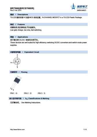
BR7N60(BRCS7N60R) Rev.C Feb.-2015 DATA SHEET / Descriptions TO-220 N MOS N-CHANNEL MOSFET in a TO-220 Plastic Package. / Features , , Low gate charge, low crss, fast switching. / Applications DC/DC These devices are well suited for high
7n60af 7n60h.pdf
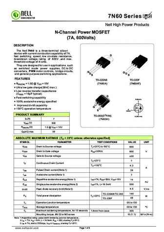
RoHS 7N60 Series RoHS SEMICONDUCTOR Nell High Power Products N-Channel Power MOSFET (7A, 600Volts) DESCRIPTION The Nell 7N60 is a three-terminal silicon device with current conduction capability of 7A, D fast switching speed, low on-state resistance, breakdown voltage rating of 600V ,and max. threshold voltage of 4 volts. They are designed for use in applications. such as sw
hfh7n60.pdf
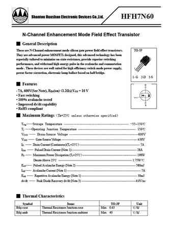
Shantou Huashan Electronic Devices Co.,Ltd. HFH7N60 N-Channel Enhancement Mode Field Effect Transistor General Description These are N-Channel enhancement mode silicon gate power field effect transistors. TO-3P They are advanced power MOSFETs designed, this advanced technology has been especially tailored to minimize on-state resistance, provide superior switching performance
hff7n60.pdf
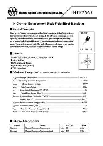
Shantou Huashan Electronic Devices Co., Ltd. HFF7N60 N-Channel Enhancement Mode Field Effect Transistor General Description These are N-Channel enhancement mode silicon gate power field effect transistors. TO-220F They are advanced power MOSFETs designed, this advanced technology has been especially tailored to minimize on-state resistance, provide superior switching performan
hfp7n60.pdf
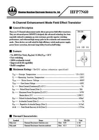
Shantou Huashan Electronic Devices Co., Ltd. HFP7N60 N-Channel Enhancement Mode Field Effect Transistor General Description These are N-Channel enhancement mode silicon gate power field effect transistors. TO-220 They are advanced power MOSFETs designed, this advanced technology has been especially tailored to minimize on-state resistance, provide superior switching performan
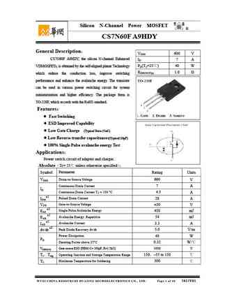
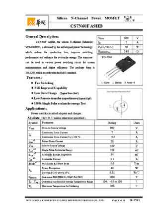
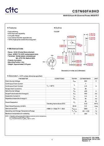
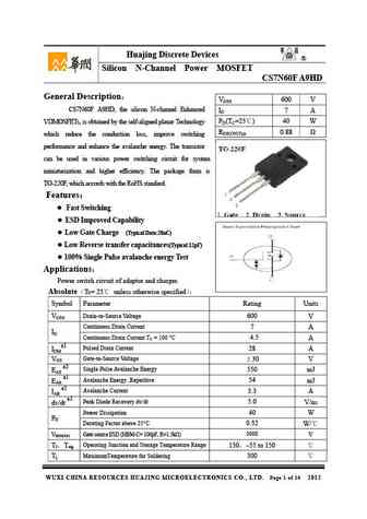
cs7n60f a9hdy.pdf
Silicon N-Channel Power MOSFET R CS7N60F A9HDY General Description VDSS 600 V CS7N60F A9HDY, the silicon N-channel Enhanced ID 7 A PD(TC=25 ) 40 W VDMOSFETs, is obtained by the self-aligned planar Technology RDS(ON)Typ 1.0 which reduce the conduction loss, improve switching performance and enhance the avalanche energy. The transistor can be used in various
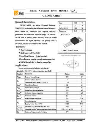
cs7n60 a8hd.pdf
Silicon N-Channel Power MOSFET R CS7N60 A8HD General Description VDSS 600 V CS7N60 A8HD, the silicon N-channel Enhanced ID 7 A PD(TC=25 ) 100 W VDMOSFETs, is obtained by the self-aligned planar Technology RDS(ON)Typ 0.88 which reduce the conduction loss, improve switching performance and enhance the avalanche energy. The transistor can be used in various pow
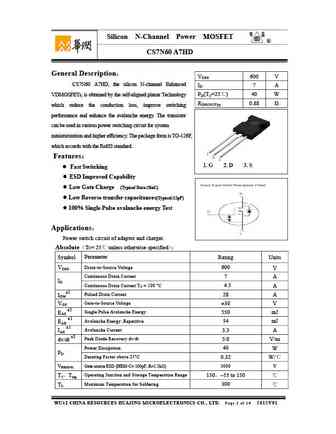
cs7n60 a7hd.pdf
Silicon N-Channel Power MOSFET R CS7N60 A7HD General Description VDSS 600 V CS7N60 A7HD, the silicon N-channel Enhanced ID 7 A PD(TC=25 ) 40 W VDMOSFETs, is obtained by the self-aligned planar Technology RDS(ON)Typ 0.88 which reduce the conduction loss, improve switching performance and enhance the avalanche energy. The transistor can be used in various pow
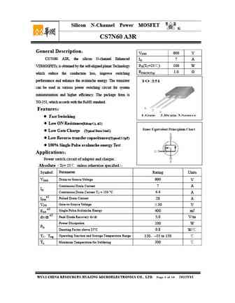
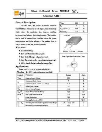
cs7n60 a3r.pdf
Silicon N-Channel Power MOSFET R CS7N60 A3R General Description VDSS 600 V CS7N60 A3R, the silicon N-channel Enhanced ID 7 A PD(TC=25 ) 100 W VDMOSFETs, is obtained by the self-aligned planar Technology RDS(ON)Typ 1.0 which reduce the conduction loss, improve switching performance and enhance the avalanche energy. The transistor can be used in various power
cs7n60f a9hd.pdf
Silicon N-Channel Power MOSFET R CS7N60F A9HD General Description VDSS 600 V CS7N60F A9HD, the silicon N-channel Enhanced ID 7 A PD(TC=25 ) 40 W VDMOSFETs, is obtained by the self-aligned planar Technology RDS(ON)Typ 0.88 which reduce the conduction loss, improve switching performance and enhance the avalanche energy. The transistor can be used in various
cs7n60 a4r.pdf
Silicon N-Channel Power MOSFET R CS7N60 A4R General Description VDSS 600 V CS7N60 A4R, the silicon N-channel Enhanced ID 7 A PD(TC=25 ) 100 W VDMOSFETs, is obtained by the self-aligned planar Technology RDS(ON)Typ 1.0 which reduce the conduction loss, improve switching performance and enhance the avalanche energy. The transistor can be used in various power
cs7n60f a9r.pdf
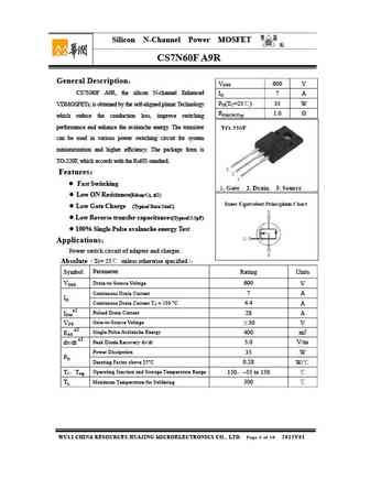
Silicon N-Channel Power MOSFET R CS7N60F A9R General Description VDSS 600 V CS7N60F A9R, the silicon N-channel Enhanced ID 7 A PD(TC=25 ) 35 W VDMOSFETs, is obtained by the self-aligned planar Technology RDS(ON)Typ 1.0 which reduce the conduction loss, improve switching performance and enhance the avalanche energy. The transistor can be used in various power
cs47n60.pdf
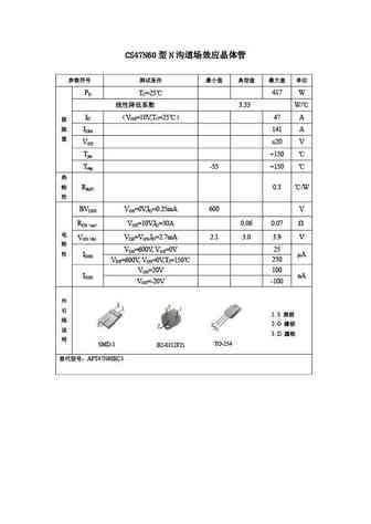
CS47N60 N PD TC=25 417 W 3.33 W/ ID VGS=10V,TC=25 47 A IDM 141 A VGS 20 V Tjm +150 Tstg -55 +150 RthJC 0.3 /W BVDSS VGS=0V,ID=0.25mA 600 V RDS on VGS=10V,ID=30A 0.06 0.07 VGS th VDS=V
cm7n60f.pdf

R CM7N60F www.jdsemi.cn ShenZhen Jingdao Electronic Co.,Ltd. POWER MOSFET 600V N-Channel VDMOS RoHS 1 LD E 2 1 2
ftk7n60p f dd.pdf
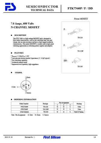
SEMICONDUCTOR FTK7N60P / F / DD TECHNICAL DATA Power MOSFET 7.0 Amps, 600 Volts N-CHANNEL MOSFET P 1 DESCRIPTION TO-220 The FTK 7N60 is a high voltage MOSFET and is designed to have better characteristics, such as fast switching time, low gate charge, low on-state resistance and have a high rugged avalanche characteristics. This power MOSFET is usually used at high speed F s
f7n60.pdf
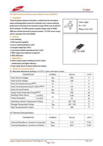
F7N60 7A 600V N-channel Enhancement Mode Power MOSFET 1 Description These N-channel enhanced vdmosfets, is obtained by the self-aligned V DSS = 600V planar technology which reduce the conduction loss, improve switching I = 7.0A D performance and enhance the avalanche energy. Which accords with the RoHS standard. TO-220F provides insulation voltage rated at 2000V R DS(on) TYP) =1.
d7n60.pdf
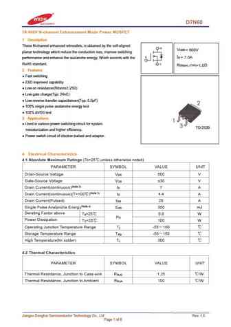
D7N60 7A 600V N-channel Enhancement Mode Power MOSFET 1 Description These N-channel enhanced vdmosfets, is obtained by the self-aligned V DSS = 600V planar technology which reduce the conduction loss, improve switching I = 7.0A D performance and enhance the avalanche energy. Which accords with the RoHS standard. R DS(on) TYP) =1.0 2 Features Fast switching ESD improv
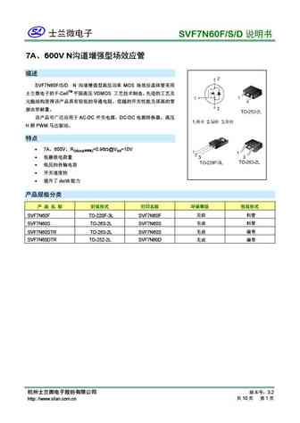
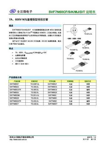
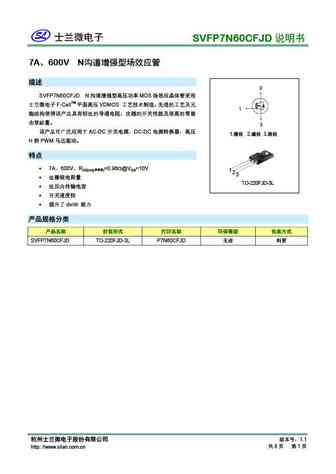
svf7n60cf svf7n60cs svf7n60ck svf7n60cmj svf7n60cd svf7n60ct.pdf
SVF7N60CF/S/K/MJ/D/T 7A 600V N SVF7N60CF/S/K/MJ/D/T N MOS F-CellTM VDMOS
svf7n60cf svf7n60cs svf7n60cstr svf7n60ck svf7n60cmj svf7n60cd svf7n60cdtr svf7n60ct.pdf
svs7n60fjd2 svs7n60dd2tr svs7n60fd2.pdf
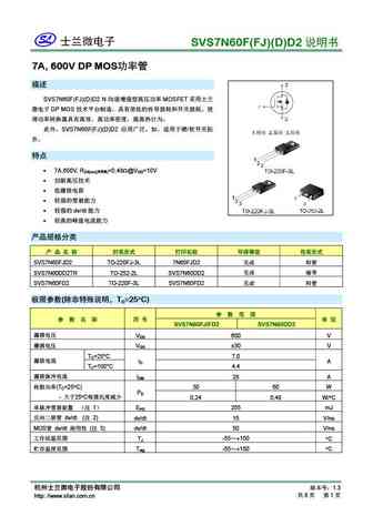
SVS7N60F(FJ)(D)D2 7A, 600V DP MOS SVS7N60F(FJ)(D)D2 N MOSFET DP MOS SVS7N60F(FJ)(D)D2 / 7A,600
svf7n60t svf7n60f.pdf
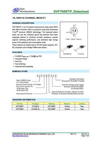
SVF7N60T/F_Datasheet 7A, 600V N-CHANNEL MOSFET GENERAL DESCRIPTION SVF7N60T/F is an N-channel enhancement mode power MOS field effect transistor which is produced using Silan proprietary F-CellTM structure VDMOS technology. The improved planar stripe cell and the improved guard ring terminal have been especially tailored to minimize on-state resistance, provide superior switching
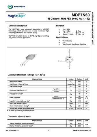
mdp7n60th.pdf
MDP7N60 N-Channel MOSFET 600V, 7A, 1.15 General Description Features The MDP7N60 uses advanced MagnaChip s MOSFET V = 600V DS Technology, which provides low on-state resistance, high V = 660V @ T DS jmax switching performance and excellent quality. I = 7.0A @ V = 10V D GS RDS(ON) 1.15 @ VGS = 10V MDP7N60 is suitable device for SMPS, high Speed switching Applica
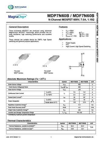
mdf7n60bth mdp7n60bth.pdf
MDP7N60B / MDF7N60B N-Channel MOSFET 600V, 7.0A, 1.15 General Description Features These N-channel MOSFET are produced using advanced V = 600V DS MagnaChip s MOSFET Technology, which provides low on- V = 660V @ T DS jmax state resistance, high switching performance and excellent I = 7.0A @ V = 10V D GS quality. RDS(ON) 1.15 @ VGS = 10V Applications These devices
ms7n60.pdf
MS7N60 N-Channel Enhancement Mode Power MOSFET Description The MS7N60 is a N-channel enhancement-mode MOSFET , providing the designer with the best combination of fast switching, ruggedized device design, low on-resistance and cost effectiveness. The TO-220 package is universally preferred for all commercial-industrial applications Features Low On Resistance Simple
msf7n60.pdf
MSF7N60 600V N-Channel MOSFET Description The MSF7N60 is a N-channel enhancement-mode MOSFET , providing the designer with the best combination of fast switching, ruggedized device design, low on-resistance and cost effectiveness. The TO-220F package is universally preferred for all commercial-industrial applications Features Low On Resistance Simple Drive Requirem
wff7n60.pdf
WFF7N60 WFF7N60 WFF7N60 WFF7N60 Silicon N-Channel MOSFET Silicon N-Channel MOSFET Silicon N-Channel MOSFET Silicon N-Channel MOSFET Features 7A,600V,R (Max 1.2 )@V =10V DS(on) GS Ultra-low Gate Charge(Typical 29nC) Fast Switching Capability 100%Avalanche Tested Isolation Voltage(V =4000V AC) ISO Maximum Junction Temperature Range(150 ) General Descri
wfp7n60.pdf
WFP7N60 WFP7N60 WFP7N60 WFP7N60 Silicon N-Channel MOSFET Silicon N-Channel MOSFET Silicon N-Channel MOSFET Silicon N-Channel MOSFET Features 7A,600V,R (Max 1.0 )@V =10V DS(on) GS Ultra-low Gate Charge(Typical 29nC) Fast Switching Capability 100%Avalanche Tested Isolation Voltage(V =4000V AC) ISO Maximum Junction Temperature Range(150 ) General Descri
sff7n60.pdf
SFF7N60 SFF7N60 SFF7N60 SFF7N60 Silicon N-Channel MOSFET Silicon N-Channel MOSFET Silicon N-Channel MOSFET Silicon N-Channel MOSFET Features 7A,600V,R (Max 1.0 )@V =10V DS(on) GS Ultra-low Gate Charge(Typical 29nC) Fast Switching Capability 100%Avalanche Tested Isolation Voltage(V =4000V AC) ISO Maximum Junction Temperature Range(150 ) General Descri
bl7n60a-p bl7n60a-a bl7n60a-u bl7n60a-d.pdf
BL7N60A Power MOSFET Power MOSFET Power MOSFET Power MOSFET 1 Description BL7N60A, the silicon N-channel Enhanced MOSFETs, is obtained by advanced MOSFET technology which reduce the conduction loss, improve switching performance and enhance the avalanche energy. The transistor is suitable device for SMPS, high speed switching and general purpose application
blv7n60.pdf
BLV7N60 N-channel Enhancement Mode Power MOSFET 600V DSS Avalanche Energy Specified BV Fast Switching RDS(ON) 1.0 Simple Drive Requirements ID 7A Description This advanced high voltage MOSFET is produced using Belling s proprietary DMOS technology. Designed for high efficiency switch mode power supply. Absolute Maximum Ratings ( TC=25oC unless
cs7n60fa9hdy.pdf
CS7N60FA9HDY 600V Silicon N-Channel Power MOSFET Features Outline Fast switching. TO-220F ESD improved capability. 0.189(4.80) 0.173(4.40) Low gate charge. 0.409(10.40) 0.378(9.60) 0.114(2.90) Low reverse transfer capacitances. 0.098(2.50) 100% single pulse avalanche energy test. 0.638(16.20) 0.606(15.40) Marking code Mechanical data G D S E
cs7n60fa9hd.pdf
CS7N60FA9HD 600V Silicon N-Channel Power MOSFET Features Outline Fast switching. TO-220F ESD improved capability. 0.189(4.80) 0.173(4.40) Low gate charge. 0.409(10.40) 0.378(9.60) 0.114(2.90) Low reverse transfer capacitances. 0.098(2.50) 100% single pulse avalanche energy test. 0.638(16.20) 0.606(15.40) Marking code Mechanical data G D S Ep
ctm07n60.pdf
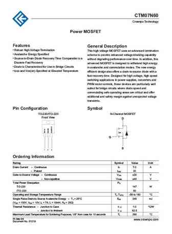
CTM07N60 Crownpo Technology Power MOSFET Features General Description Robust High Voltage Termination This high voltage MOSFET uses an advanced termination Avalanche Energy Specified scheme to provide enhanced voltage-blocking capability Source-to-Drain Diode Recovery Time Comparable to a without degrading performance over time. In addition, this Discrete Fast Recovery
fhp7n60a fhf7n60a.pdf
N N-CHANNEL MOSFET FHP7N60A /FHF7N60A MAIN CHARACTERISTICS FEATURES ID 7A Low gate charge VDSS 600V Crss ( 5.5pF) Low Crss (typical 5.5pF ) Rdson-typ @Vgs=10V 0.9 Fast switching Qg-typ 24nC 100% 100% avalanche tested dv/dt Impr
cs7n60f.pdf
BRF7N60(CS7N60F) N-Channel MOSFET/N MOS DC/DC Purpose These devices are well suited for high efficiency switching DC/DC converters and switch mode power supplies. , , Features Low gate charge, low crss, fast switching. /Absolute maximum ratings(Ta=25 )
jfpc7n60c jffm7n60c.pdf
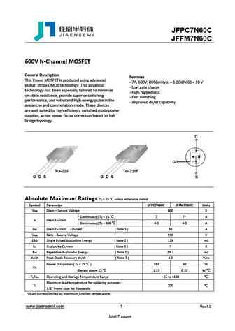
JFPC7N60C JFFM7N60C 600V N-Channel MOSFET General Description Features This Power MOSFET is produced using advanced - 7A, 600V, RDS(on)typ. = 1.2 @VGS = 10 V planar stripe DMOS technology. This advanced - Low gate charge technology has been especially tailored to minimize - High ruggedness on-state resistance, provide superior switching - Fast switching performance, a
kia7n60u.pdf
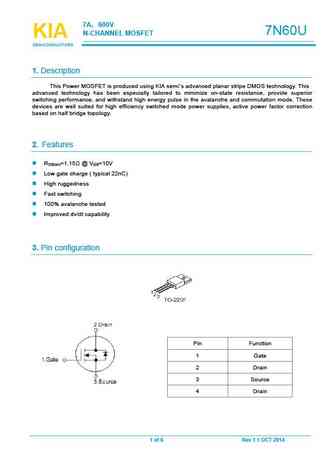
7A 600V 7N60U N-CHANNELMOSFET KIA KIA KIA SEMICONDUCTORS SEMICONDUCTORS SEMICONDUCTORS 1.Description This Power MOSFETis produced using KIAsemi s advancedplanar stripeDMOStechnology. This advanced technology has been especially tailored to minimize on-state resistance, provide superior switching performance, and withstand high energy pulse in the avalanche and commutation mode. Th
kia7n60h.pdf
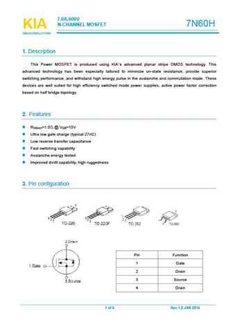
7.0A,600V N-CHANNELMOSFET 7N60H KIA KIA KIA SEMICONDUCTORS SEMICONDUCTORS SEMICONDUCTORS 1.Description This Power MOSFET is produced using KIA s advanced planar stripe DMOS technology. This advanced technology has been especially tailored to minimize on-state resistance, provide superior switching performance, and withstand high energy pulse in the avalanche and commutation mode. Th
slp7n60c slf7n60c.pdf
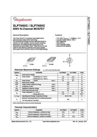
SLP7N60C / SLF7N60C 600V N-Channel MOSFET General Description Features This Power MOSFET is produced using Maple semi s - 7.0A, 600V, RDS(on)Typ. = 1.0 @VGS = 10 V advanced planar stripe DMOS technology. - Low gate charge ( typical 25nC) This advanced technology has been especially tailored to - High ruggedness minimize on-state resistance, provide superior switching - Fast switching
swf7n60k swi7n60k.pdf
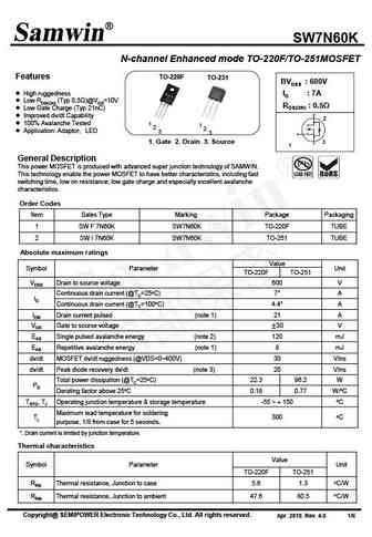
SW7N60K N-channel Enhanced mode TO-220F/TO-251MOSFET Features TO-220F TO-251 BVDSS 600V High ruggedness ID 7A Low RDS(ON) (Typ 0.5 )@VGS=10V RDS(ON) 0.5 Low Gate Charge (Typ 21nC) Improved dv/dt Capability 2 100% Avalanche Tested 1 1 2 2 Application Adaptor LED 3 3 3 1. Gate 2. Drain 3. Source 1 General Descr
sw7n60d swf7n60d swp7n60d swi7n60d swd7n60d.pdf
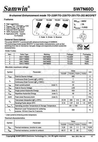
SW7N60D N-channel Enhancement mode TO-220F/TO-220/TO-251/TO-252 MOSFET Features TO-220F TO-220 TO-251 TO-252 BVDSS 600V High ruggedness ID 7A RDS(ON) (Typ 1.05 )@VGS=10V RDS(ON) 1.05 Gate Charge (Typ 30nC) Improved dv/dt Capability 2 100% Avalanche Tested 1 1 1 1 2 2 2 2 Application UPS Inverter 3 3 3 3 TV
swf7n60d swp7n60d swi7n60d swd7n60d.pdf
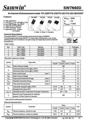
SW7N60D N-channel Enhancement mode TO-220F/TO-220/TO-251/TO-252 MOSFET Features TO-220F TO-220 TO-251 TO-252 BVDSS 600V High ruggedness ID 7A Low RDS(ON) (Typ 1.05 )@VGS=10V RDS(ON) 1.05 Low Gate Charge (Typ 30nC) Improved dv/dt Capability 2 100% Avalanche Tested 1 1 1 1 2 2 2 2 Application UPS Inverter 3 3 3
swt47n60k.pdf
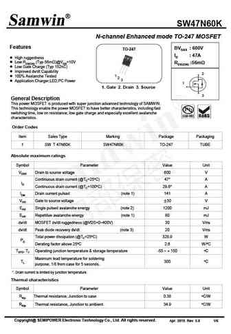
SW47N60K N-channel Enhanced mode TO-247 MOSFET Features BVDSS 600V TO-247 ID 47A High ruggedness Low RDS(ON) (Typ 56m )@VGS=10V RDS(ON) 56m Low Gate Charge (Typ 152nC) Improved dv/dt Capability 2 1 100% Avalanche Tested 2 3 Application Charger,LED,PC Power 1 1. Gate 2. Drain 3. Source 3 General Description This power MO
swd7n60k2f.pdf
SW7N60K2F N-channel Enhanced mode TO-252 MOSFET TO-252 BVDSS 600V Features ID 7A High ruggedness RDS(ON) 0.43 Low RDS(ON) (Typ 0.43 )@VGS=10V Low Gate Charge (Typ 13nC) 2 Improved dv/dt Capability 1 100% Avalanche Tested 2 1 3 Application LED , Adaptor, Charger 1. Gate 2. Drain 3. Source 3 General Description This pow
srm7n60.pdf
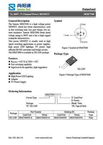
Datasheet 7A, 600V, N-Channel Power MOSFET SRM7N60 General Description Symbol The Sanrise SRM7N60 is a high voltage power MOSFET, which has better characteristics, such as fast switching time, low gate charge, low on- state resistance. Sanrise SRM7N60 break down voltage rating is 600V and it has a high rugged avalanche characteristics. This power MOSFET is usually used at high
msu7n60f msu7n60t.pdf
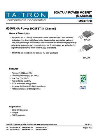
600V/7.4A POWER MOSFET (N-Channel) MSU7N60 600V/7.4A Power MOSFET (N-Channel) General Description MSU7N60 is a N-Channel enhancement mode power MOSFET with advanced TO-220 technology. It is designed to have better characteristics, such as fast switching time, low gate charge, minimized on-state resistance and withstanding high energy pulse in the avalanche and commutati
tmd7n60z tmu7n60z.pdf
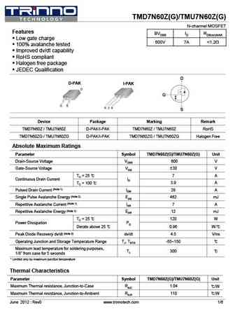
TMD7N60Z(G)/TMU7N60Z(G) N-channel MOSFET Features BVDSS ID RDS(on)MAX Low gate charge 600V 7A
tmp7n60z tmpf7n60z.pdf
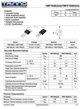
TMP7N60Z(G)/TMPF7N60Z(G) N-channel MOSFET Features BVDSS ID RDS(on) Low gate charge 600V 7A
tsp7n60m tsf7n60m.pdf
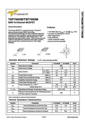
TSP7N60M/TSF7N60M 600V N-Channel MOSFET General Description Features This Power MOSFET is produced using Truesemi s 7.0A,600V,Max.RDS(on)=1.3 @ VGS =10V advanced planar stripe DMOS technology. This advanced technology has been especially tailored to Low gate charge(typical 29nC) minimize on-state resistance, provide superior switching High ruggedness performance, and
qm07n60f.pdf
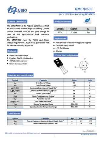
QM07N60F 1 2011-04-29 - 1 - N-Ch 600V Fast Switching MOSFETs General Description Product Summery The QM07N60F is the highest performance N-ch MOSFETs with extreme high cell density , which BVDSS RDSON ID provide excellent RDSON and gate charge for 600V 1.35 7A most of the synchronous buck converter applications . Applications The QM07N60F meet the RoHS and
wmm07n60c4 wml07n60c4 wmo07n60c4 wmn07n60c4 wmp07n60c4 wmk07n60c4.pdf
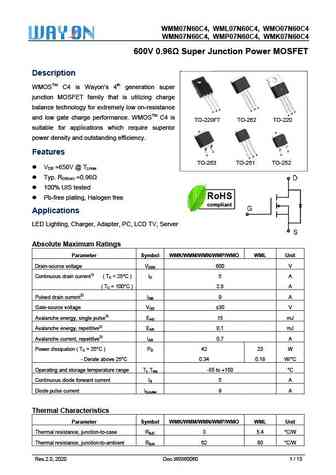
WMM0 60C4, MO07N60C 07N60C4, WML07N6 WM C4 WMN0 60C4, MK07N60C 07N60C4, WMP07N6 WM C4 600V 0.96 S T V Super Junction Power MOSFET Descrip ption WMOSTM C4 is Wa 4th generation super ayon s n junction MOSFET fa that is utilizing charge M amily S balance te or extremely esistance echnology fo y low on-re D S D G G G S D G and low ga charge performanc WM
cs7n60fa9hd.pdf
Huajing Discrete Devices R Silicon N-Channel Power MOSFET CS7N60F A9HD General Description VDSS 600 V CS7N60F A9HD, the silicon N-channel Enhanced ID 7 A PD(TC=25 ) 40 W VDMOSFETs, is obtained by the self-aligned planar Technology RDS(ON)Typ 0.88 which reduce the conduction loss, improve switching performance and enhance the avalanche energy. The transistor
cs7n60a7hd.pdf

Silicon N-Channel Power MOSFET R CS7N60 A7HD General Description VDSS 600 V CS7N60 A7HD, the silicon N-channel Enhanced ID 7 A PD(TC=25 ) 40 W VDMOSFETs, is obtained by the self-aligned planar Technology RDS(ON)Typ 0.88 which reduce the conduction loss, improve switching performance and enhance the avalanche energy. The transistor can be used in various pow
cs7n60a8hd.pdf

Silicon N-Channel Power MOSFET R CS7N60 A8HD General Description VDSS 600 V CS7N60 A8HD, the silicon N-channel Enhanced ID 7 A PD(TC=25 ) 100 W VDMOSFETs, is obtained by the self-aligned planar Technology RDS(ON)Typ 0.88 which reduce the conduction loss, improve switching performance and enhance the avalanche energy. The transistor can be used in various pow
cs7n60cf cs7n60cp cs7n60cu cs7n60cd.pdf
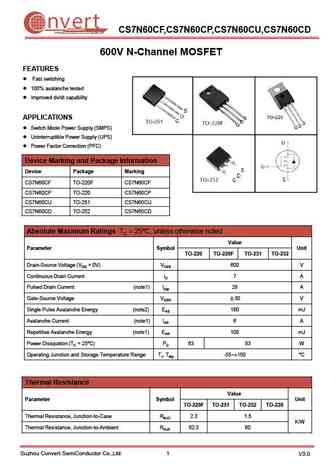
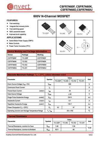
nvert CS7N60CF,CS7N60CP,CS7N60CU,CS7N60CD Suzhou Convert Semiconductor Co ., Ltd. 600V N-Channel MOSFET FEATURES Fast switching 100% avalanche tested Improved dv/dt capability APPLICATIONS Switch Mode Power Supply (SMPS) Uninterruptible Power Supply (UPS) Power Factor Correction (PFC) Device Marking and Package Information Device Package Marking CS7N60CF TO
cs7n60f cs7n60p.pdf
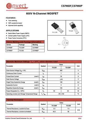
CS7N60F,CS7N60P nvert Suzhou Convert Semiconductor Co ., Ltd. 600V N-Channel MOSFET FEATURES Fast switching 100% avalanche tested Improved dv/dt capability APPLICATIONS Switch Mode Power Supply (SMPS) Uninterruptible Power Supply (UPS) Power Factor Correction (PFC) Device Marking and Package Information Device Package Marking CS7N60F TO-220F CS7N60F CS7N60
csfr7n60f csfr7n60k csfr7n60d csfr7n60u.pdf
CSFR7N60F, CSFR7N60K, nvert Suzhou Convert Semiconductor Co ., Ltd. CSFR7N60D,CSFR7N60U 600V N-Channel MOSFET FEATURES Fast switching Integrate fast recovery diode Fast switching speed 100% avalanche tested Improved dv/dt capability APPLICATIONS Switch Mode Power Supply (SMPS) Motor Controls Power Factor Correction (PFC) Device Marking and Package
fir7n60fg.pdf
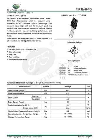
FIR7N60FG Advanced N-Ch Power MOSFET-I General Description PIN Connection TO-220F FIR7N60FG is an N-channel enhancement mode power MOS field effect transistor which is produced using proprietary F-CellTM structure VDMOS technology. The improved planar stripe cell and the improved guard ring terminal have been especially tailored to minimize on-state resistance, provide superior swit
smf7n60.pdf
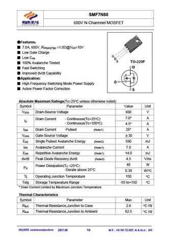
SMF7N60 600V N-Channnel MOSFET Features 7.0A, 600V, R =1.0 @V =10V DS(on)(Typ) GS Low Gate Charge Low C rss 100% Avalanche Tested Fast Switching Improved dv/dt Capability Application High Frequency Switching Mode Power Supply Active Power Factor Correction Absolute Maximum Ratings(Tc=25 C unless otherwise noted) Symbol Parameter Value
lnc7n60d lnd7n60d lng7n60d lnh7n60d.pdf
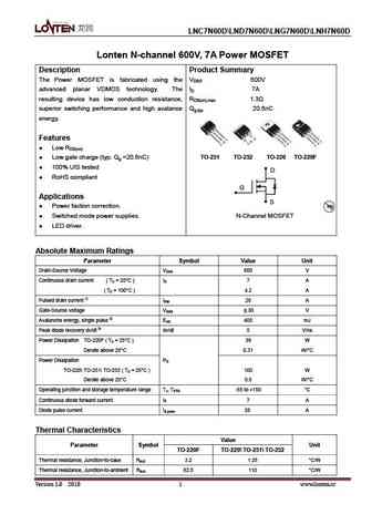
LNC7N60D LND7N60D LNG7N60D LNH7N60D Lonten N-channel 600V, 7A Power MOSFET Description Product Summary The Power MOSFET is fabricated using the VDSS 600V advanced planar VDMOS technology. The ID 7A resulting device has low conduction resistance, RDS(on),max 1.3 superior switching performance and high avalance Qg,typ 20.6nC energy. Features Low RDS(on) Low gate cha
lnc7n60 lnd7n60.pdf
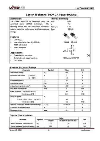
LNC7N60 LND7N60 Lonten N-channel 600V, 7A Power MOSFET Description Product Summary The Power MOSFET is fabricated using the VDSS 600V advanced planar VDMOS technology. The ID 7A resulting device has low conduction resistance, RDS(on),max 1.3 superior switching performance and high avalance Qg,typ 20.6nC energy. Features Low RDS(on) Low gate charge (typ. Qg =20.6nC
ssw47n60s ssa47n60s.pdf
SUPER-SEMI SUPER-MOSFET Super Junction Metal Oxide Semiconductor Field Effect Transistor 600V Super Junction Power MOSFET SS*47N60S Rev. 1.3 Jun. 2019 www.supersemi.com.cn March, 2016 SJ-FET SSW47N60S/SSA47N60S 600V N-Channel MOSFET Description Features SJ-FET is new generation of high voltage MOSFET family that is utilizing an advanced charge balance mechanism fo
ssw47n60sfd ssa47n60sfd.pdf
SUPER-SEMI SUPER-MOSFET Super Junction Metal Oxide Semiconductor Field Effect Transistor 600V Super Junction Power MOSFET With Fast-Recovery SS*47N60SFD Rev. 1.5 Jun. 2019 www.supersemi.com.cn March, 2016 SJ-FET SSW47N60SFD/SSA47N60SFD 600V N-Channel MOSFET With Fast-Recovery Description Features SJ-FET is new generation of high voltage MOSFET family that Mult
tma7n60h tmc7n60h tmd7n60h tmu7n60h.pdf
TMA7N60H, TMC7N60H, TMD7N60H, TMU7N60H Wuxi Unigroup Microelectronics Company 600V N-Channel MOSFET FEATURES Fast switching 100% avalanche tested Improved dv/dt capability APPLICATIONS Switch Mode Power Supply (SMPS) Uninterruptible Power Supply (UPS) Power Factor Correction (PFC) Device Marking and Package Information Device Package Marking TM
hm7n60k hm7n60i.pdf
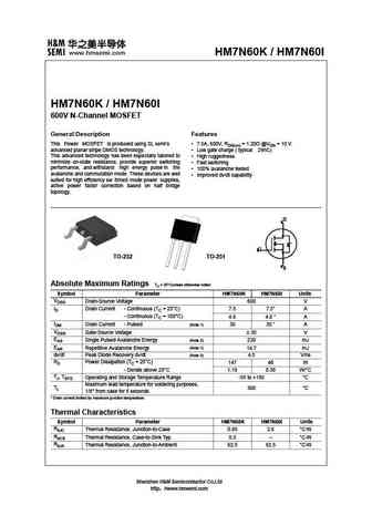
HM7N60K / HM7N60I HM7N60K / HM7N60I 600V N-Channel MOSFET General Description Features This Power MOSFET is produced using SL semi s 7.5A, 600V, RDS(on) = 1.20 @VGS = 10 V advanced planar stripe DMOS technology. Low gate charge ( typical 29nC) This advanced technology has been especially tailored to High ruggedness minimize on-state resistance, provide superior switchin
hms47n60a.pdf
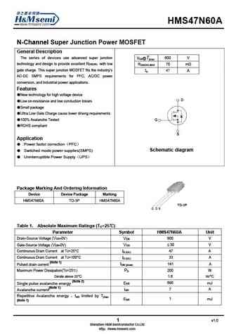
HMS47N60A N-Channel Super Junction Power MOSFET General Description The series of devices use advanced super junction 600 V VDS@Tjmax technology and design to provide excellent RDS(ON) with low RDS(ON) MAX 70 m gate charge. This super junction MOSFET fits the industry s ID A AC-DC SMPS requirements for PFC, AC/DC power conversion, and industrial power applications. Fea
hm7n60 hm7n60f.pdf
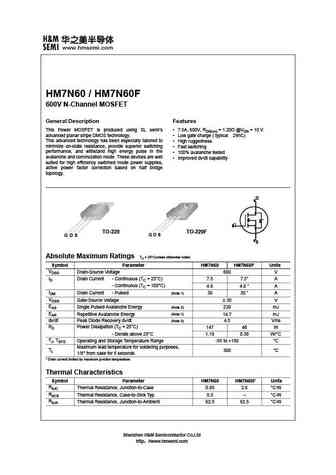
HM7N60 / HM7N60F 600V N-Channel MOSFET General Description Features This Power MOSFET is produced using SL semi s 7.5A, 600V, RDS(on) = 1.20 @VGS = 10 V advanced planar stripe DMOS technology. Low gate charge ( typical 29nC) This advanced technology has been especially tailored to High ruggedness minimize on-state resistance, provide superior switching Fast switchin
h7n60p h7n60f.pdf
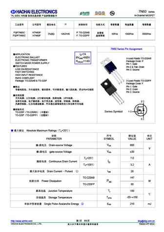
7N60 Series N-Channel MOSFET 7A, 600V, N H FQP7N60C H7N60P P TO-220AB HAOHAI 50Pcs 1000Pcs 5000Pcs 7N60 FQPF7N60C H7N60F F TO-220FP 7N60 Series Pin Assignment APPLICATION ID=7A ELECTRONIC BALLAST
spb07n60c3.pdf
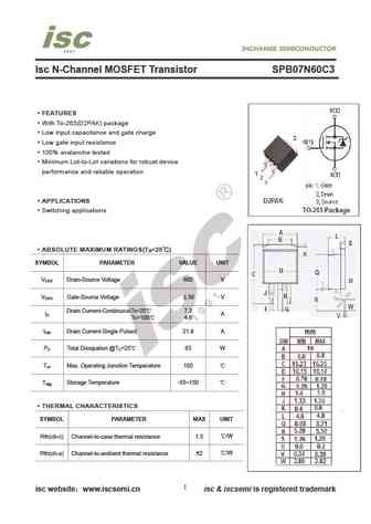
Isc N-Channel MOSFET Transistor SPB07N60C3 FEATURES With To-263(D2PAK) package Low input capacitance and gate charge Low gate input resistance 100% avalanche tested Minimum Lot-to-Lot variations for robust device performance and reliable operation APPLICATIONS Switching applications ABSOLUTE MAXIMUM RATINGS(T =25 ) a SYMBOL PARAMETER VALUE UNIT V Drain-Source Vo
spw47n60cfd.pdf
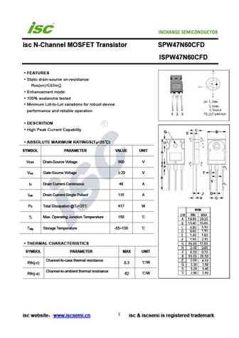
INCHANGE Semiconductor isc N-Channel MOSFET Transistor SPW47N60CFD ISPW47N60CFD FEATURES Static drain-source on-resistance RDS(on) 83m Enhancement mode 100% avalanche tested Minimum Lot-to-Lot variations for robust device performance and reliable operation DESCRITION High Peak Current Capability ABSOLUTE MAXIMUM RATINGS(T =25 ) a SYMBOL PARAMETER VALUE UNI
spw47n60c3.pdf
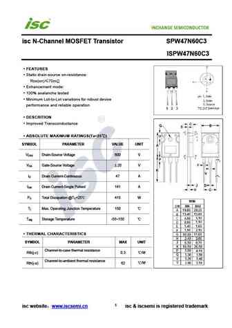
isc N-Channel MOSFET Transistor SPW47N60C3 ISPW47N60C3 FEATURES Static drain-source on-resistance RDS(on) 70m Enhancement mode 100% avalanche tested Minimum Lot-to-Lot variations for robust device performance and reliable operation DESCRITION Improved Transconductance ABSOLUTE MAXIMUM RATINGS(T =25 ) a SYMBOL PARAMETER VALUE UNIT V Drain-Source Voltage 600
spu07n60c3.pdf
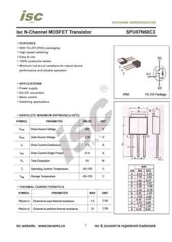
isc N-Channel MOSFET Transistor SPU07N60C3 FEATURES With TO-251(IPAK) packaging High speed switching Easy to use 100% avalanche tested Minimum Lot-to-Lot variations for robust device performance and reliable operation APPLICATIONS Power supply DC-DC converters Motor control Switching applications ABSOLUTE MAXIMUM RATINGS(T =25 ) a SYMBOL PARAMETER VALUE
spd07n60s5.pdf
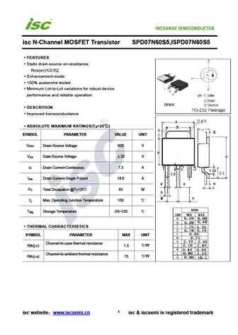
isc N-Channel MOSFET Transistor SPD07N60S5,ISPD07N60S5 FEATURES Static drain-source on-resistance RDS(on) 0.6 Enhancement mode 100% avalanche tested Minimum Lot-to-Lot variations for robust device performance and reliable operation DESCRITION Improved transconductance ABSOLUTE MAXIMUM RATINGS(T =25 ) a SYMBOL PARAMETER VALUE UNIT V Drain-Source Voltage 600
aotf7n60.pdf
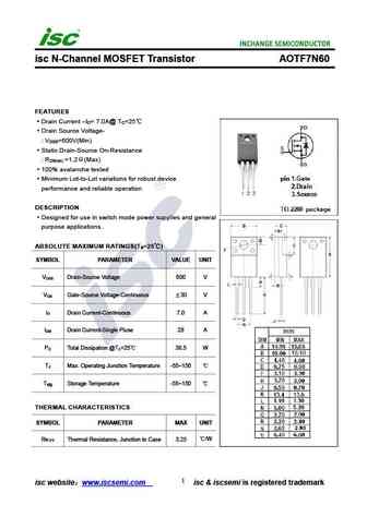
isc N-Channel MOSFET Transistor AOTF7N60 FEATURES Drain Current I = 7.0A@ T =25 D C Drain Source Voltage- V =600V(Min) DSS Static Drain-Source On-Resistance R =1.2 (Max) DS(on) 100% avalanche tested Minimum Lot-to-Lot variations for robust device performance and reliable operation DESCRIPTION Designed for use in switch mode power supplies and general purpos
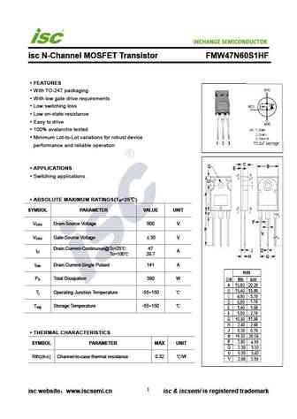
apt47n60bc3.pdf
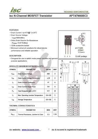
isc N-Channel MOSFET Transistor APT47N60BC3 FEATURES Drain Current I =47A@ T =25 D C Drain Source Voltage- V =600V(Min) DSS Static Drain-Source On-Resistance R =0.07 (Max) DS(on) 100% avalanche tested Minimum Lot-to-Lot variations for robust device performance and reliable operation DESCRIPTION Designed for use in switch mode power supplies and general purp
spp07n60cfd.pdf
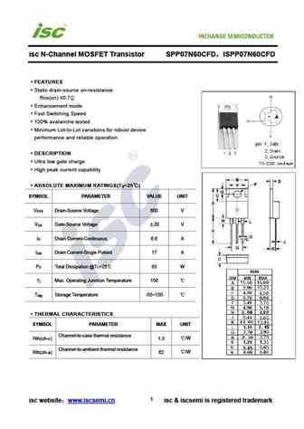
isc N-Channel MOSFET Transistor SPP07N60CFD ISPP07N60CFD FEATURES Static drain-source on-resistance RDS(on) 0.7 Enhancement mode Fast Switching Speed 100% avalanche tested Minimum Lot-to-Lot variations for robust device performance and reliable operation DESCRIPTION Ultra low gate charge High peak current capability ABSOLUTE MAXIMUM RATINGS(T =25 ) a
aotf7n60fd.pdf
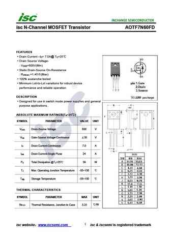
isc N-Channel MOSFET Transistor AOTF7N60FD FEATURES Drain Current I = 7.0A@ T =25 D C Drain Source Voltage- V =600V(Min) DSS Static Drain-Source On-Resistance R =1.45 (Max) DS(on) 100% avalanche tested Minimum Lot-to-Lot variations for robust device performance and reliable operation DESCRIPTION Designed for use in switch mode power supplies and general pur
spb07n60s5.pdf

Isc N-Channel MOSFET Transistor SPB07N60S5 FEATURES With To-263(D2PAK) package Low input capacitance and gate charge Low gate input resistance 100% avalanche tested Minimum Lot-to-Lot variations for robust device performance and reliable operation APPLICATIONS Switching applications ABSOLUTE MAXIMUM RATINGS(T =25 ) a SYMBOL PARAMETER VALUE UNIT V Drain-Source Vo
spa07n60cfd.pdf
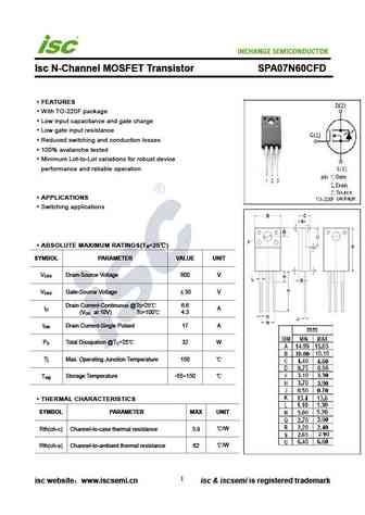
INCHANGE Semiconductor Isc N-Channel MOSFET Transistor SPA07N60CFD FEATURES With TO-220F package Low input capacitance and gate charge Low gate input resistance Reduced switching and conduction losses 100% avalanche tested Minimum Lot-to-Lot variations for robust device performance and reliable operation APPLICATIONS Switching applications ABSOLUTE MAXIMUM RATING
mdp7n60th.pdf
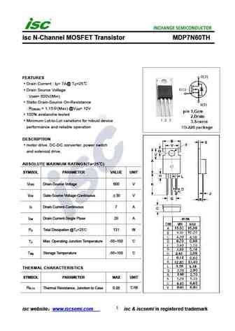
isc N-Channel MOSFET Transistor MDP7N60TH FEATURES Drain Current I = 7A@ T =25 D C Drain Source Voltage V = 600V(Min) DSS Static Drain-Source On-Resistance R = 1.15 (Max) @V = 10V DS(on) GS 100% avalanche tested Minimum Lot-to-Lot variations for robust device performance and reliable operation DESCRIPTION motor drive, DC-DC converter, power switch and soleno
spu07n60s5.pdf

isc N-Channel MOSFET Transistor SPU07N60S5 FEATURES With TO-251(IPAK) packaging High speed switching Easy to use 100% avalanche tested Minimum Lot-to-Lot variations for robust device performance and reliable operation APPLICATIONS Power supply DC-DC converters Motor control Switching applications ABSOLUTE MAXIMUM RATINGS(T =25 ) a SYMBOL PARAMETER VALUE
aot7n60.pdf
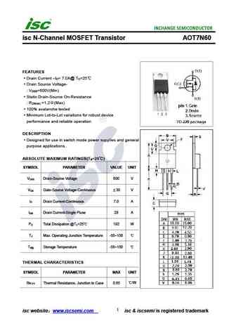
isc N-Channel MOSFET Transistor AOT7N60 FEATURES Drain Current I = 7.0A@ T =25 D C Drain Source Voltage- V =600V(Min) DSS Static Drain-Source On-Resistance R =1.2 (Max) DS(on) 100% avalanche tested Minimum Lot-to-Lot variations for robust device performance and reliable operation DESCRIPTION Designed for use in switch mode power supplies and general purpose
spp07n60c3.pdf

isc N-Channel MOSFET Transistor SPP07N60C3 ISPP07N60C3 FEATURES Static drain-source on-resistance RDS(on) 0.6 Enhancement mode Fast Switching Speed 100% avalanche tested Minimum Lot-to-Lot variations for robust device performance and reliable operation DESCRIPTION Ultra low gate charge High peak current capability Improved transconductance ABSOLUTE MA
apt77n60bc6.pdf
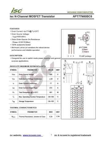
isc N-Channel MOSFET Transistor APT77N60BC6 FEATURES Drain Current I =77A@ T =25 D C Drain Source Voltage- V =600V(Min) DSS Static Drain-Source On-Resistance R =0.041 (Max) DS(on) 100% avalanche tested Minimum Lot-to-Lot variations for robust device performance and reliable operation DESCRIPTION Designed for use in switch mode power supplies and general pur
aoi7n60.pdf
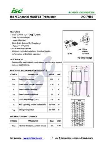
isc N-Channel MOSFET Transistor AOI7N60 FEATURES Drain Current I = 7.0A@ T =25 D C Drain Source Voltage- V =600V(Min) DSS Static Drain-Source On-Resistance R =1.3 (Max) DS(on) 100% avalanche tested Minimum Lot-to-Lot variations for robust device performance and reliable operation DESCRIPTION Designed for use in switch mode power supplies and general purpose
sihg47n60aef.pdf
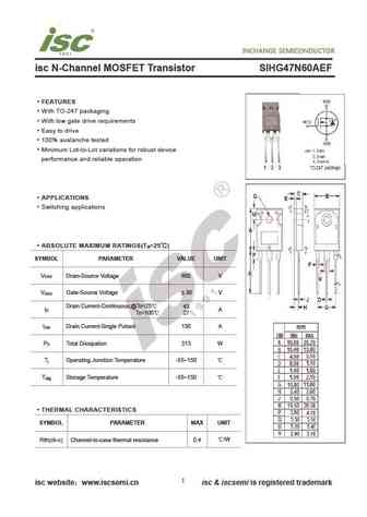
isc N-Channel MOSFET Transistor SIHG47N60AEF FEATURES With TO-247 packaging With low gate drive requirements Easy to drive 100% avalanche tested Minimum Lot-to-Lot variations for robust device performance and reliable operation APPLICATIONS Switching applications ABSOLUTE MAXIMUM RATINGS(T =25 ) a SYMBOL PARAMETER VALUE UNIT V Drain-Source Voltage 600 V DSS V
17n60.pdf
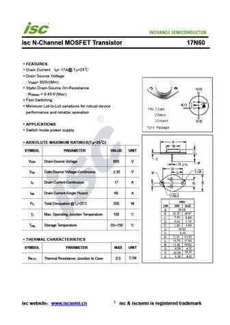
isc N-Channel MOSFET Transistor 17N60 FEATURES Drain Current I = 17A@ T =25 D C Drain Source Voltage V = 600V(Min) DSS Static Drain-Source On-Resistance R = 0.45 (Max) DS(on) Fast Switching Minimum Lot-to-Lot variations for robust device performance and reliable operation APPLICATIONS Switch mode power supply. ABSOLUTE MAXIMUM RATINGS(T =25 ) a SYMBO
irfp27n60k.pdf
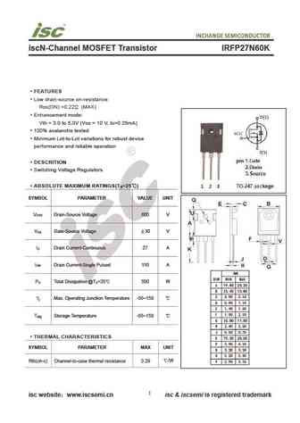
iscN-Channel MOSFET Transistor IRFP27N60K FEATURES Low drain-source on-resistance RDS(ON) =0.22 (MAX) Enhancement mode Vth = 3.0 to 5.0V (VDS = 10 V, ID=0.25mA) 100% avalanche tested Minimum Lot-to-Lot variations for robust device performance and reliable operation DESCRITION Switching Voltage Regulators ABSOLUTE MAXIMUM RATINGS(T =25 ) a SYMBOL PARAMETER VAL
fmh47n60s1fd.pdf
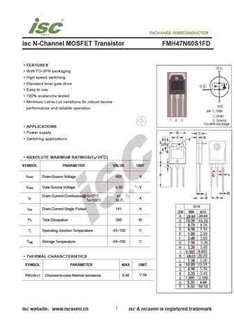
isc N-Channel MOSFET Transistor FMH47N60S1FD FEATURES With TO-3PN packaging High speed switching Standard level gate drive Easy to use 100% avalanche tested Minimum Lot-to-Lot variations for robust device performance and reliable operation APPLICATIONS Power supply Switching applications ABSOLUTE MAXIMUM RATINGS(T =25 ) a SYMBOL PARAMETER VALUE UNIT V Drai
aod7n60.pdf
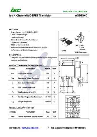
isc N-Channel MOSFET Transistor AOD7N60 FEATURES Drain Current I = 7.0A@ T =25 D C Drain Source Voltage- V =600V(Min) DSS Static Drain-Source On-Resistance R =1.3 (Max) DS(on) 100% avalanche tested Minimum Lot-to-Lot variations for robust device performance and reliable operation DESCRIPTION Designed for use in switch mode power supplies and general purpose
fdpf7n60nz.pdf
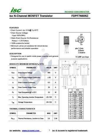
isc N-Channel MOSFET Transistor FDPF7N60NZ FEATURES Drain Current I = 6.5A@ T =25 D C Drain Source Voltage- V = 600V(Min) DSS Static Drain-Source On-Resistance R = 1.25 (Max) DS(on) 100% avalanche tested Minimum Lot-to-Lot variations for robust device performance and reliable operation DESCRIPTION Designed for use in switch mode power supplies and general p
sss7n60b.pdf
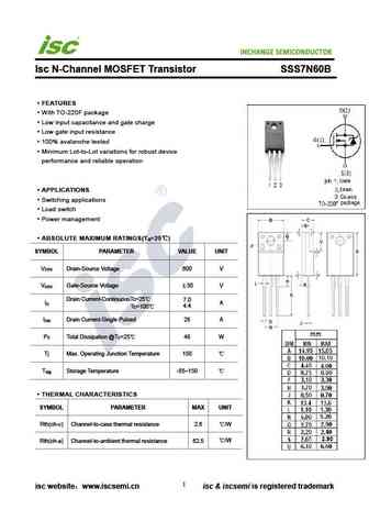
INCHANGE Semiconductor Isc N-Channel MOSFET Transistor SSS7N60B FEATURES With TO-220F package Low input capacitance and gate charge Low gate input resistance 100% avalanche tested Minimum Lot-to-Lot variations for robust device performance and reliable operation APPLICATIONS Switching applications Load switch Power management ABSOLUTE MAXIMUM RATINGS(T =25 )
spp07n60s5.pdf
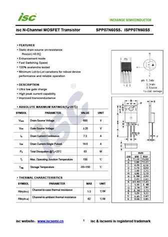
isc N-Channel MOSFET Transistor SPP07N60S5 ISPP07N60S5 FEATURES Static drain-source on-resistance RDS(on) 0.6 Enhancement mode Fast Switching Speed 100% avalanche tested Minimum Lot-to-Lot variations for robust device performance and reliable operation DESCRIPTION Ultra low gate charge High peak current capability Improved transconductance ABSOLUTE MA
spd07n60c3.pdf
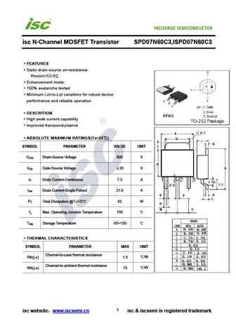
isc N-Channel MOSFET Transistor SPD07N60C3,ISPD07N60C3 FEATURES Static drain-source on-resistance RDS(on) 0.6 Enhancement mode 100% avalanche tested Minimum Lot-to-Lot variations for robust device performance and reliable operation DESCRITION High peak current capability Improved transconductance ABSOLUTE MAXIMUM RATINGS(T =25 ) a SYMBOL PARAMETER VALUE U
fdd7n60nz.pdf
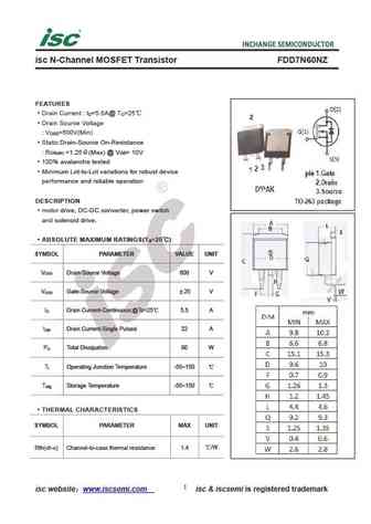
isc N-Channel MOSFET Transistor FDD7N60NZ FEATURES Drain Current I =5.5A@ T =25 D C Drain Source Voltage V =600V(Min) DSS Static Drain-Source On-Resistance R =1.25 (Max) @ V = 10V DS(on) GS 100% avalanche tested Minimum Lot-to-Lot variations for robust device performance and reliable operation DESCRIPTION motor drive, DC-DC converter, power switch and soleno
7n60gs 7n60ds.pdf
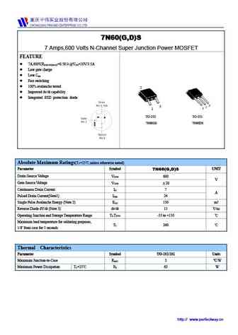
7N60(G,D)S 7 Amps,600 Volts N-Channel Super Junction Power MOSFET FEATURE 7A,600V,R =0.58 @V =10V/3.5A DS(ON)MAX GS Low gate charge Low C iss Fast switching 100% avalanche tested Improved dv/dt capability Integrated ESD protection diode TO-252 TO-251 7N60GS 7N60DS Absolute Maximum Ratings(T =25 ,unless otherwise noted) C Parameter Symbol UNIT 7N60
47n60ys.pdf
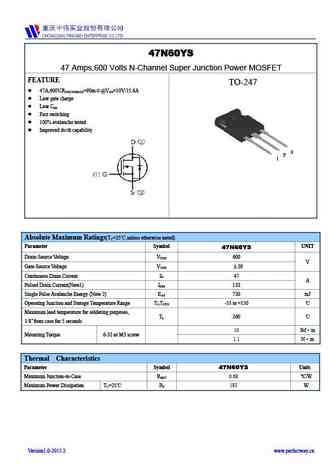
47N60YS 47 Amps,600 Volts N-Channel Super Junction Power MOSFET FEATURE TO-247 47A,600V,R =90m @V =10V/15.6A DS(ON)MAX GS Low gate charge Low C iss Fast switching 100% avalanche tested Improved dv/dt capability Absolute Maximum Ratings(T =25 ,unless otherwise noted) C Parameter Symbol UNIT 47N60YS Drain-Source Voltage V 600 DSS V Gate-Source Voltage
7n60tf.pdf
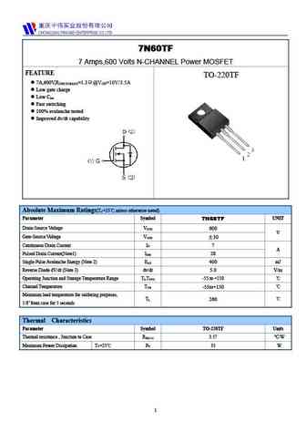
7N60TF 7 Amps,600 Volts N-CHANNEL Power MOSFET FEATURE TO-220TF 7A,600V,R =1.3 @V =10V/3.5A DS(ON)MAX GS Low gate charge Low C iss Fast switching 100% avalanche tested Improved dv/dt capability Absolute Maximum Ratings(T =25 ,unless otherwise noted) C Parameter Symbol UNIT 7N60TF Drain-Source Voltage V 600 DSS V Gate-Source Voltage V 30 GSS Cont
Другие MOSFET... 4N65K , 5N65 , 5N65K , 6N65 , 5N60 , 6N60 , 6N60Z , 7N60A , IRFB7545 , 7N60Z , 7N60K , 8N60 , 10N60 , 10N60K , 12N60 , 15N60 , 18N60 .
🌐 : EN ES РУ

Список транзисторов
Обновления
MOSFET: ASD80R750E | ASD70R950E | ASD70R600E | ASD70R380E | ASD65R850E | ASD65R550E | ASD65R350E | ASD65R300E | ASD65R280E | ASD65R270E | ASD60R330E | ASD60R280E | ASB80R750E | ASB70R380E | ASB65R300E | ASB65R220E
Popular searches
2sc1111 | bc239 transistor equivalent | 3sk41 | 2sc2240 transistor | c3198 | 2sc793 | 2sd313 replacement | 2n4249