8N60 datasheet, аналоги, основные параметры
Наименование производителя: 8N60 📄📄
Тип транзистора: MOSFET
Полярность: N
Предельные значения
Pd ⓘ - Максимальная рассеиваемая мощность: 147 W
|Vds|ⓘ - Максимально допустимое напряжение сток-исток: 600 V
|Vgs|ⓘ - Максимально допустимое напряжение затвор-исток: 30 V
|Id| ⓘ - Максимально допустимый постоянный ток стока: 8 A
Tj ⓘ - Максимальная температура канала: 150 °C
Электрические характеристики
tr ⓘ - Время нарастания: 60.5 ns
Cossⓘ - Выходная емкость: 105 pf
RDSonⓘ - Сопротивление сток-исток открытого транзистора: 1 Ohm
📄📄 Копировать
Аналог (замена) для 8N60
- подборⓘ MOSFET транзистора по параметрам
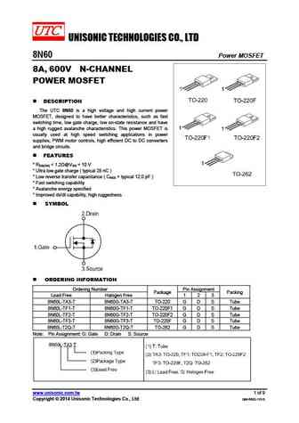
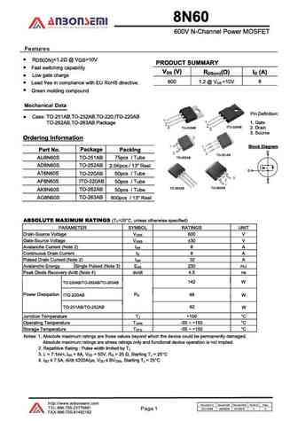
8N60 даташит
8n60.pdf
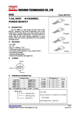
UNISONIC TECHNOLOGIES CO., LTD 8N60 Power MOSFET 7.5A, 600V N-CHANNEL POWER MOSFET DESCRIPTION The UTC 8N60 is a high voltage and high current power MOSFET, designed to have better characteristics, such as fast switching time, low gate charge, low on-state resistance and have a high rugged avalanche characteristics. This power MOSFET is usually used at high speed switching a
8n60 8n60f.pdf
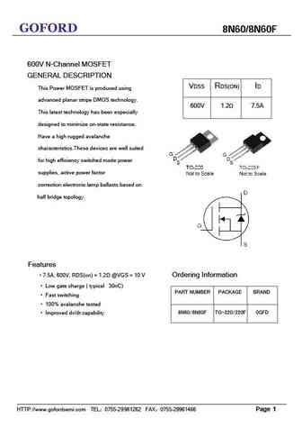
GOFORD 8N60/8N60F 600V N-Channel MOSFET GENERAL DESCRIPTION VDSS RDS(ON) ID This Power MOSFET is produced using advanced planar stripe DMOS technology. 600V 1.2 7.5A This latest technology has been especially designed to minimize on-state resistance, Have a high rugged avalanche characteristics.These devices are well suited for high efficiency switched mode power supplies, active
8n60.pdf
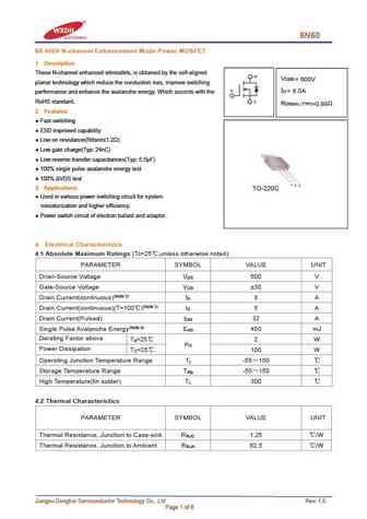
8N60 8A 600V N-channel Enhancement Mode Power MOSFET 1 Description These N-channel enhanced vdmosfets, is obtained by the self-aligned V DSS = 600V planar technology which reduce the conduction loss, improve switching I = 8.0A D performance and enhance the avalanche energy. Which accords with the RoHS standard. R DS(on) TYP) =0.98 2 Features Fast switching ESD improv
8n60.pdf
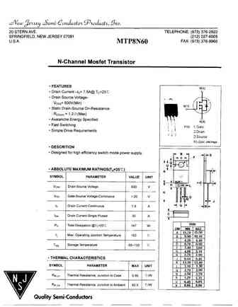
INCHANGE Semiconductor isc Product Specification isc N-Channel Mosfet Transistor 8N60 FEATURES Drain Current ID= 7.5A@ TC=25 Drain Source Voltage- VDSS= 600V(Min) Static Drain-Source On-Resistance RDS(on) = 1.2 (Max) Avalanche Energy Specified Fast Switching Simple Drive Requirements DESCRITION Designed for high efficiency switch mode power
ndf08n60zg ndp08n60zg.pdf
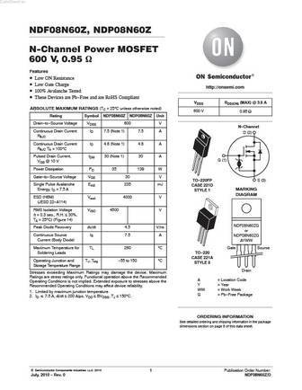
DataSheet.in NDF08N60Z, NDP08N60Z N-Channel Power MOSFET 600 V, 0.95 W Features Low ON Resistance Low Gate Charge http //onsemi.com 100% Avalanche Tested These Devices are Pb-Free and are RoHS Compliant VDSS RDS(ON) (MAX) @ 3.5 A ABSOLUTE MAXIMUM RATINGS (TC = 25 C unless otherwise noted) 600 V 0.95 W Rating Symbol NDF08N60Z NDP08N60Z Unit Drain-to-Source Voltage
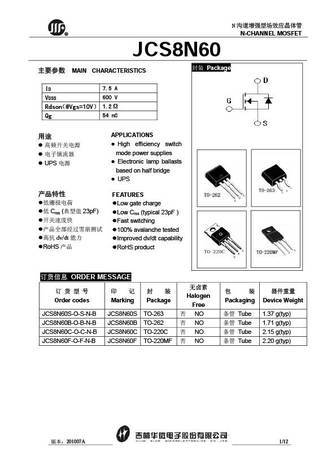
jcs8n60s jcs8n60b jcs8n60c jcs8n60f.pdf
N R N-CHANNEL MOSFET JCS8N60 Package MAIN CHARACTERISTICS 7.5 A ID 600 V VDSS Rdson 1.2 @Vgs=10V 54 nC Qg APPLICATIONS High efficiency switch mode power supplies Electronic lamp ballasts UPS based on half bridge UPS FEA
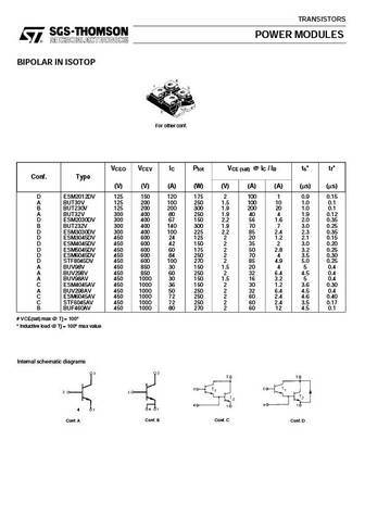
ste24n90 ste36n50-da ste36n50-dk ste38n60 ste38na50 ste45n50 ste50n40 ste90n25.pdf
TRANSISTORS POWER MODULES BIPOLAR IN ISOTOP For other conf. VCEO VCEV IC Ptot VCE (sat) @IC / IB ts* tf* Conf. Type (V) (V) (A) (W) (V) (A) (A) ( s) ( s) D ESM2012DV 125 150 120 175 2 100 1 0.9 0.15 A BUT30V 125 200 100 250 1.5 100 10 1.0 0.1 B BUT230V 125 200 200 300 1.9 200 20 1.0 0.1 A BUT32V 300 400 80 250 1.9 40 4 1.9 0.12 D ESM2030DV 300 400 67 150 2.2 56 1.6 2.0 0.35 B BUT2
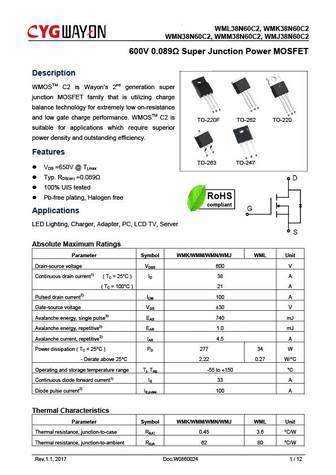
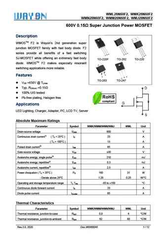
wml38n60c2 wmk38n60c2 wmn38n60c2 wmm38n60c2 wmj38n60c2.pdf
WML38N MK38N60C N60C2, WM C2 WMN38N60C2, WMM38N MJ38N60C N60C2, WM C2 600V 0.089 S 0 Super Junction Power MOSFET Descrip ption WMOSTM C2 is Wa 2nd generation super ayon s n junction MOSFET fa that is utilizing charge M amily S balance te or extremely esistance echnology fo y low on-re S D D G G G S D G and low ga charge performanc WMOSTM C2 is ate ce
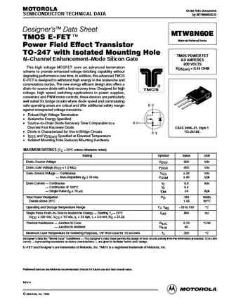
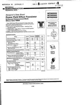
mtw8n60e.pdf
MOTOROLA Order this document SEMICONDUCTOR TECHNICAL DATA by MTW8N60E/D Designer's Data Sheet MTW8N60E TMOS E-FET. Motorola Preferred Device Power Field Effect Transistor TO-247 with Isolated Mounting Hole TMOS POWER FET N Channel Enhancement Mode Silicon Gate 8.0 AMPERES 600 VOLTS This high voltage MOSFET uses an advanced termination RDS(on) = 0.55 OHM scheme to provid
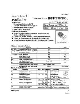
irfps38n60l.pdf
PD - 94630 SMPS MOSFET IRFPS38N60L Applications HEXFET Power MOSFET Zero Voltage Switching SMPS Trr typ. VDSS RDS(on) typ. ID Telecom and Server Power Supplies Uninterruptible Power Supplies 600V 120m 170ns 38A Motor Control applications Features and Benefits SuperFast body diode eliminates the need for external diodes in ZVS applications. Lower Gate c
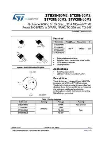
stb28n60m2 sti28n60m2 stp28n60m2 stw28n60m2.pdf
STB28N60M2, STI28N60M2, STP28N60M2, STW28N60M2 N-channel 600 V, 0.135 typ., 22 A MDmesh M2 Power MOSFETs in D PAK, I PAK, TO-220 and TO-247 Datasheet - production data Features Order code V @ T R max. I DS Jmax DS(on) D STB28N60M2 STI28N60M2 650 V 0.150 22 A STP28N60M2 STW28N60M2 Extremely low gate charge Excellent output capacitance (C ) profile
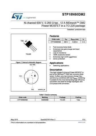
stp18n60dm2.pdf
STP18N60DM2 N-channel 600 V, 0.260 typ., 12 A MDmesh DM2 Power MOSFET in a TO-220 package Datasheet - production data Features Order code V R max. I DS DS(on) D STP18N60DM2 600 V 0.295 12 A Fast-recovery body diode Extremely low gate charge and input capacitance Low on-resistance 100% avalanche tested Extremely high dv/dt ruggedness Ze
stfh18n60m2.pdf
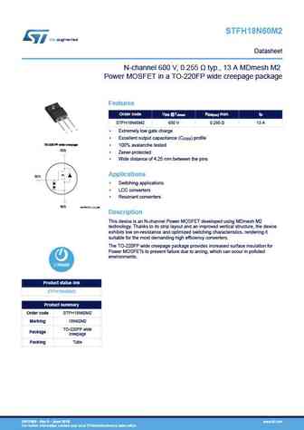
STFH18N60M2 Datasheet N-channel 600 V, 0.255 typ., 13 A MDmesh M2 Power MOSFET in a TO-220FP wide creepage package Features VDS @TJmax RDS(on) max. ID Order code STFH18N60M2 650 V 0.280 13 A Extremely low gate charge Excellent output capacitance (COSS) profile TO-220 FP wide creepage 100% avalanche tested D(2) Zener-protected Wide distance of 4.25 mm bet
stw48n60m2-4.pdf
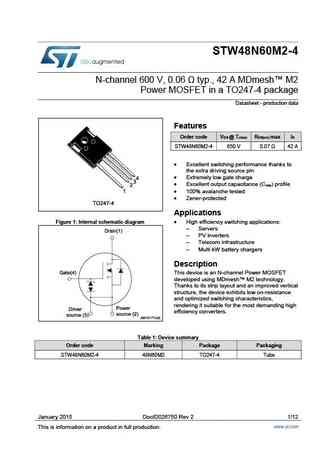
STW48N60M2-4 N-channel 600 V, 0.06 typ., 42 A MDmesh M2 Power MOSFET in a TO247-4 package Datasheet - production data Features Order code V Jmax DS(on) D DS @ T R max I STW48N60M2-4 650 V 0.07 42 A Excellent switching performance thanks to the extra driving source pin Extremely low gate charge Excellent output capacitance (C ) profile oss 100% a
stw48n60m6-4.pdf
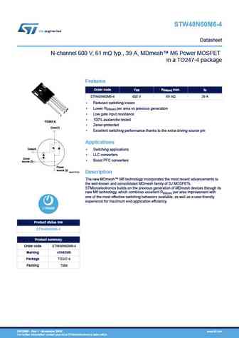
STW48N60M6-4 Datasheet N-channel 600 V, 61 m typ., 39 A, MDmesh M6 Power MOSFET in a TO247 4 package Features VDS RDS(on) max. ID Order code STW48N60M6-4 600 V 69 m 39 A Reduced switching losses Lower RDS(on) per area vs previous generation 4 3 2 Low gate input resistance 1 100% avalanche tested TO247-4 Zener-protected Drain(1) Excellent swit
stb18n60m2 stp18n60m2 stw18n60m2.pdf
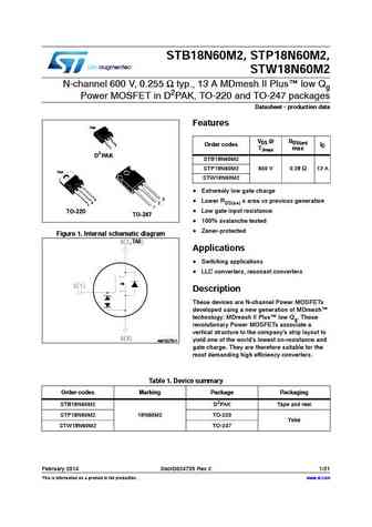
STB18N60M2, STP18N60M2, STW18N60M2 N-channel 600 V, 0.255 typ., 13 A MDmesh II Plus low Qg Power MOSFET in D2PAK, TO-220 and TO-247 packages Datasheet - production data Features TAB VDS @ RDS(on) 3 Order codes ID 1 TJmax max 2 D PAK STB18N60M2 STP18N60M2 650 V 0.28 13 A TAB STW18N60M2 Extremely low gate charge 3 3 Lower RDS(on) x area vs previous generation
stf28n60dm2.pdf
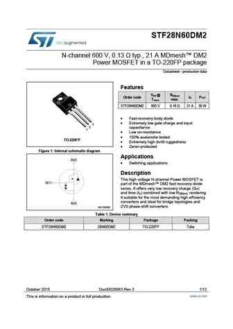
STF28N60DM2 N-channel 600 V, 0.13 typ., 21 A MDmesh DM2 Power MOSFET in a TO-220FP package Datasheet - production data Features V @ R DS DS(on) Order code I P D TOT T max. Jmax. STF28N60DM2 650 V 0.16 21 A 30 W Fast-recovery body diode Extremely low gate charge and input 3 2 capacitance 1 Low on-resistance 100% avalanche tested TO-220F
stw48n60m2.pdf
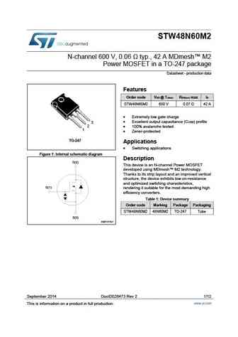
STW48N60M2 N-channel 600 V, 0.06 typ., 42 A MDmesh M2 Power MOSFET in a TO-247 package Datasheet - production data Features Order code V Jmax DS(on) D DS @ T R max I STW48N60M2 650 V 0.07 42 A Extremely low gate charge Excellent output capacitance (C ) profile OSS 3 2 100% avalanche tested 1 Zener-protected TO-247 Applications Switchin
stf8n60dm2.pdf
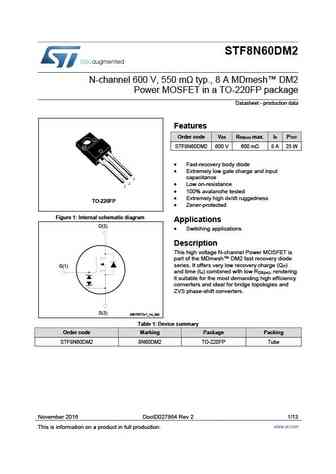
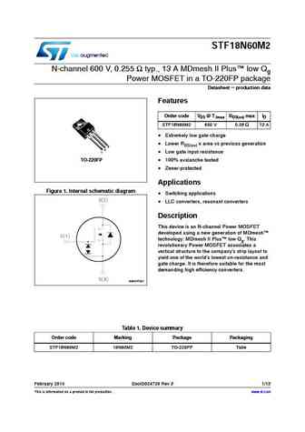
STF8N60DM2 N-channel 600 V, 550 m typ., 8 A MDmesh DM2 Power MOSFET in a TO-220FP package Datasheet - production data Features Order code V R max. I P DS DS(on) D TOT STF8N60DM2 600 V 600 m 8 A 25 W Fast-recovery body diode Extremely low gate charge and input capacitance Low on-resistance 100% avalanche tested Extremely high dv/dt ruggedness
stb28n60m2 stp28n60m2 stw28n60m2.pdf
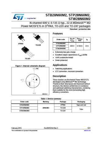
STB28N60M2, STP28N60M2, STW28N60M2 N-channel 600 V, 0.135 typ., 22 A MDmesh M2 Power MOSFETs in D2PAK, TO-220 and TO-247 packages Datasheet - production data TAB Features TAB VDS @ RDS(on) Order code ID 3 TJmax max 1 3 2 1 STB28N60M2 D2PAK TO-220 STP28N60M2 650 V 0.150 22 A STW28N60M2 Extremely low gate charge 3 Excellent output capacitance (Coss) prof
stf18n60m2.pdf
STF18N60M2 N-channel 600 V, 0.255 typ., 13 A MDmesh II Plus low Qg Power MOSFET in a TO-220FP package Datasheet - production data Features Order code VDS @ TJmax RDS(on) max ID STF18N60M2 650 V 0.28 13 A Extremely low gate charge Lower RDS(on) x area vs previous generation 3 2 1 Low gate input resistance TO-220FP 100% avalanche tested Zener-protected
stwa48n60dm2.pdf
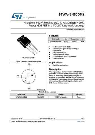
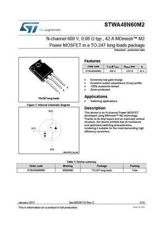
STWA48N60DM2 N-channel 600 V, 0.065 typ., 40 A MDmesh DM2 Power MOSFET in a TO-247 long leads package Datasheet - production data Features Order code V R max. I DS DS(on) D STWA48N60DM2 600 V 0.079 40 A Fast-recovery body diode Extremely low gate charge and input capacitance Low on-resistance 100% avalanche tested Extremely high dv/dt rugged
stb28n60dm2 stp28n60dm2 stw28n60dm2.pdf
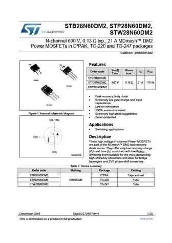
STB28N60DM2, STP28N60DM2, STW28N60DM2 N-channel 600 V, 0.13 typ., 21 A MDmesh DM2 Power MOSFETs in D PAK, TO-220 and TO-247 packages Datasheet - production data Features V @ R DS DS(on) Order code I P D TOT T max. Jmax. STB28N60DM2 STP28N60DM2 600 V 0.16 21 A 170 W STW28N60DM2 Fast-recovery body diode Extremely low gate charge and input capacita
std8n60dm2.pdf
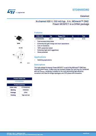
STD8N60DM2 Datasheet N-channel 600 V, 550 m typ., 8 A, MDmesh DM2 Power MOSFET in a DPAK package Features VDS RDS(on) max. ID PTOT Order code TAB STD8N60DM2 600 V 600 m 8 A 85 W 3 2 1 Fast-recovery body diode DPAK Extremely low gate charge and input capacitance Low on-resistance D(2, TAB) 100% avalanche tested Extremely high dv/dt ruggedness Ze
stwa48n60m2.pdf
STWA48N60M2 N-channel 600 V, 0.06 typ., 42 A MDmesh M2 Power MOSFET in a TO-247 long leads package Datasheet - production data Features Order code V DS @ TJmax. RDS(on) max. ID STWA48N60M2 650 V 0.07 42 A Extremely low gate charge Excellent output capacitance (C ) profile OSS 100% avalanche tested Zener-protected Applications Switching app
stf28n60m2 stfi28n60m2.pdf
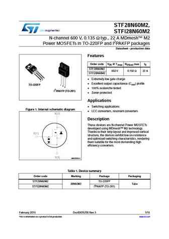
STF28N60M2, STFI28N60M2 N-channel 600 V, 0.135 typ., 22 A MDmesh M2 Power MOSFETs in TO-220FP and I2PAKFP packages Datasheet - production data Features Order code VDS @ TJmax RDS(on) max ID STF28N60M2 650 V 0.150 22 A STFI28N60M2 3 Extremely low gate charge 2 1 Excellent output capacitance (Coss) profile TO-220FP 1 2 3 100% avalanche tested 2 I PAKFP
stw48n60dm2.pdf
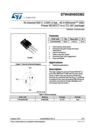
STW48N60DM2 N-channel 600 V, 0.065 typ., 40 A MDmesh DM2 Power MOSFET in a TO-247 package Datasheet - production data Features Order code V R max. I DS DS(on) D STW48N60DM2 600 V 0.079 40 A Fast-recovery body diode Extremely low gate charge and input 3 capacitance 2 Low on-resistance 1 100% avalanche tested Extremely high dv/dt ruggedness
stw48n60m6.pdf
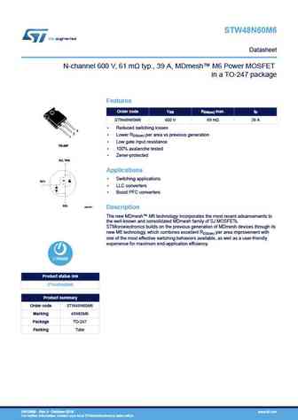
STW48N60M6 Datasheet N-channel 600 V, 61 m typ., 39 A, MDmesh M6 Power MOSFET in a TO 247 package Features VDS RDS(on) max. ID Order code STW48N60M6 600 V 69 m 39 A Reduced switching losses 3 2 Lower RDS(on) per area vs previous generation 1 Low gate input resistance TO-247 100% avalanche tested Zener-protected D(2, TAB) Applications Switchin
stl18n60m2.pdf
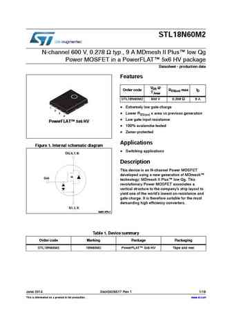
STL18N60M2 N-channel 600 V, 0.278 typ., 9 A MDmesh II Plus low Qg Power MOSFET in a PowerFLAT 5x6 HV package Datasheet - production data Features VDS @ Order code TJmax RDS(on) max ID STL18N60M2 650 V 0.308 9 A Extremely low gate charge 1 2 3 Lower RDS(on) x area vs previous generation 4 Low gate input resistance PowerFLAT 5x6 HV 100% avalanche
fqb8n60cf fqb8n60cftm.pdf
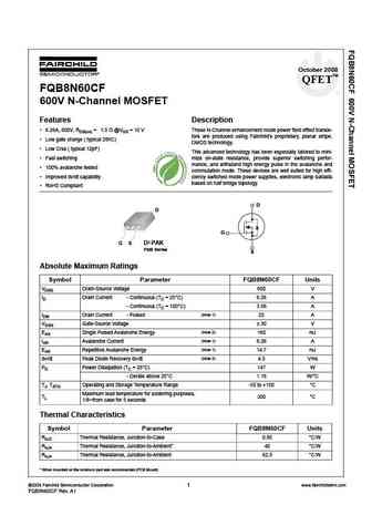
October 2008 TM QFET FQB8N60CF 600V N-Channel MOSFET Features Description 6.26A, 600V, RDS(on) = 1.5 @VGS = 10 V These N-Channel enhancement mode power field effect transis- tors are produced using Fairchild s proprietary, planar stripe, Low gate charge ( typical 28nC) DMOS technology. Low Crss ( typical 12pF) This advanced technology has been especially tailored to
fqb8n60c fqi8n60c fqi8n60ctu.pdf
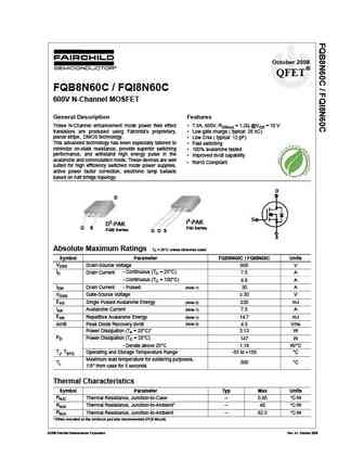
October 2008 QFET FQB8N60C / FQI8N60C 600V N-Channel MOSFET General Description Features These N-Channel enhancement mode power field effect 7.5A, 600V, RDS(on) = 1.2 @VGS = 10 V transistors are produced using Fairchild s proprietary, Low gate charge ( typical 28 nC) planar stripe, DMOS technology. Low Crss ( typical 12 pF) This advanced technology has been especiall
fqp8n60c fqpf8n60c.pdf
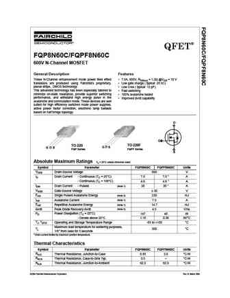
QFET FQP8N60C/FQPF8N60C 600V N-Channel MOSFET General Description Features These N-Channel enhancement mode power field effect 7.5A, 600V, RDS(on) = 1.2 @VGS = 10 V transistors are produced using Fairchild s proprietary, Low gate charge ( typical 28 nC) planar stripe, DMOS technology. Low Crss ( typical 12 pF) This advanced technology has been especially tailored to
fqpf8n60cf.pdf
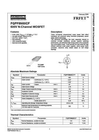
February 2006 TM FRFET FQPF8N60CF 600V N-Channel MOSFET Features Description 6.26A, 600V, RDS(on) = 1.5 @VGS = 10 V These N-Channel enhancement mode power field effect Low gate charge ( typical 28 nC) transistors are produced using Fairchild s proprietary, planar stripe, DMOS technology. Low Crss ( typical 12 pF) This advanced technology has been especially tailored t
fqp8n60c.pdf
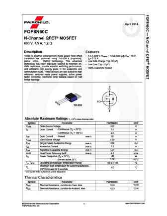
April 2014 FQP8N60C N-Channel QFET MOSFET 600 V, 7.5 A, 1.2 Description Features These N-Channel enhancement mode power field effect 7.5 A, 600 V, RDS(on) = 1.2 (Max.) @ VGS = 10 V, transistors are produced using Fairchild s proprietary, ID = 3.75 A planar stripe, DMOS technology. This advanced Low Gate Charge (Typ. 28 nC) technology has been especially tailored to mi
fqpf8n60ct fqpf8n60cydtu.pdf
QFET FQP8N60C/FQPF8N60C 600V N-Channel MOSFET General Description Features These N-Channel enhancement mode power field effect 7.5A, 600V, RDS(on) = 1.2 @VGS = 10 V transistors are produced using Fairchild s proprietary, Low gate charge ( typical 28 nC) planar stripe, DMOS technology. Low Crss ( typical 12 pF) This advanced technology has been especially tailored to
fdp8n60zu fdpf8n60zut.pdf
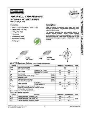
April 2009 UniFETTM FDP8N60ZU / FDPF8N60ZUT N-Channel MOSFET, FRFET 600V, 6.5A, 1.35 Features Description RDS(on) = 1.15m ( Typ.) @ VGS = 10V, ID = 3.25A These N-Channel enhancement mode power field effect transistors are produced using Fairchild s proprietary, planar Low gate charge ( Typ. 20nC) stripe, DMOS technology. Low Crss ( Typ. 10pF) This advanced techno
irfps38n60l sihfps38n60l.pdf
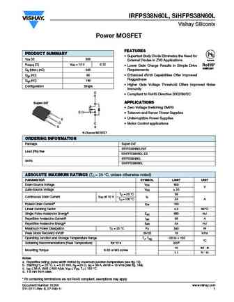
IRFPS38N60L, SiHFPS38N60L Vishay Siliconix Power MOSFET FEATURES PRODUCT SUMMARY Superfast Body Diode Eliminates the Need for VDS (V) 600 Available External Diodes in ZVS Applications RDS(on) ( )VGS = 10 V 0.12 RoHS* Lower Gate Charge Results in Simple Drive COMPLIANT Qg (Max.) (nC) 320 Requirements Qgs (nC) 85 Enhanced dV/dt Capabilities Offer Improved Ruggedness
sihp28n60ef.pdf
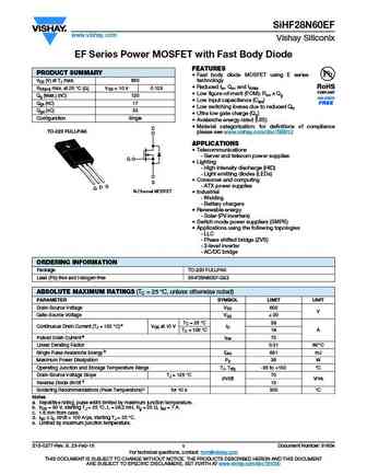
SiHP28N60EF www.vishay.com Vishay Siliconix EF Series Power MOSFET with Fast Body Diode FEATURES PRODUCT SUMMARY Fast body diode MOSFET using E series VDS (V) at TJ max. 650 technology Reduced trr, Qrr, and IRRM RDS(on) max. at 25 C ( ) VGS = 10 V 0.123 Low figure-of-merit (FOM) Ron x Qg Qg (Max.) (nC) 120 Low input capacitance (Ciss) Qgs (nC) 17 Low switc
irfps38n60l irfps38n60lpbf sihfps38n60l.pdf
IRFPS38N60L, SiHFPS38N60L Vishay Siliconix Power MOSFET FEATURES PRODUCT SUMMARY Superfast Body Diode Eliminates the Need for VDS (V) 600 Available External Diodes in ZVS Applications RDS(on) ( )VGS = 10 V 0.12 RoHS* Lower Gate Charge Results in Simple Drive COMPLIANT Qg (Max.) (nC) 320 Requirements Qgs (nC) 85 Enhanced dV/dt Capabilities Offer Improved Ruggedness
sihf28n60ef.pdf
SiHF28N60EF www.vishay.com Vishay Siliconix EF Series Power MOSFET with Fast Body Diode FEATURES PRODUCT SUMMARY Fast body diode MOSFET using E series VDS (V) at TJ max. 650 technology Reduced trr, Qrr, and IRRM RDS(on) max. at 25 C ( ) VGS = 10 V 0.123 Low figure-of-merit (FOM) Ron x Qg Qg (Max.) (nC) 120 Low input capacitance (Ciss) Qgs (nC) 17 Low switc
sihb28n60ef.pdf
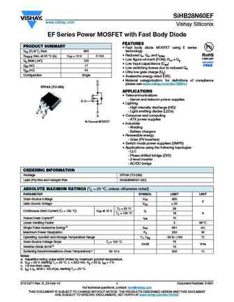
SiHB28N60EF www.vishay.com Vishay Siliconix EF Series Power MOSFET with Fast Body Diode FEATURES PRODUCT SUMMARY Fast body diode MOSFET using E series VDS (V) at TJ max. 650 technology Reduced trr, Qrr, and IRRM RDS(on) max. at 25 C ( ) VGS = 10 V 0.123 Low figure-of-merit (FOM) Ron x Qg Qg (Max.) (nC) 120 Low input capacitance (Ciss) Qgs (nC) 17 Low switc
sihg28n60ef.pdf
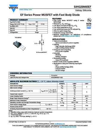
SiHG28N60EF www.vishay.com Vishay Siliconix EF Series Power MOSFET with Fast Body Diode FEATURES PRODUCT SUMMARY Fast body diode MOSFET using E series VDS (V) at TJ max. 650 technology Reduced trr, Qrr, and IRRM RDS(on) max. at 25 C ( ) VGS = 10 V 0.123 Low figure-of-merit (FOM) Ron x Qg Qg (Max.) (nC) 120 Low input capacitance (Ciss) Qgs (nC) 17 Low switc
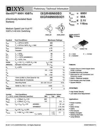
ixgr48n60b3d1.pdf
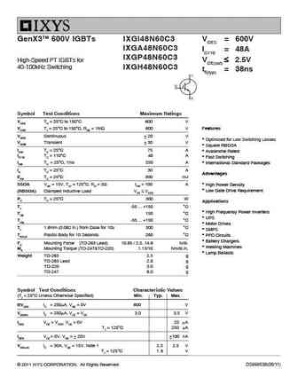
Preliminary Technical Information VCES = 600V GenX3TM 600V IGBTs IXGR48N60B3 IC25 = 60A IXGR48N60B3D1 (Electrically Isolated Back VCE(sat) 2.1V Surface) tfi(typ) = 116ns Medium-Speed Low-Vsat PT IGBTs 5-40 kHz Switching ISOPLUS247TM IXGR_B3 IXGR_B3D1 E153432 Symbol Test Conditions Maximum Ratings VCES TC = 25 C to 150 C 600 V VCGR TJ = 25 C to 150
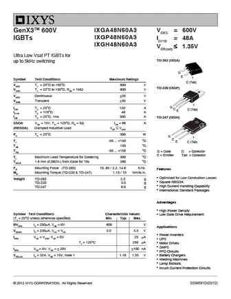
ixga48n60c3-ixgh48n60c3-ixgp48n60c3.pdf
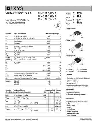
IXGA48N60C3 VCES = 600V GenX3TM 600V IGBT IXGH48N60C3 IC110 = 48A IXGP48N60C3 VCE(sat) 2.5V High Speed PT IGBTs for tfi(typ) = 38ns 40-100kHz switching TO-263 (IXGA) Symbol Test Conditions Maximum Ratings G VCES TC = 25 C to 150 C 600 V E (TAB) VCGR TJ = 25 C to 150 C, RGE = 1M 600 V TO-247 (IXGH) VGES Continuous 20 V VGEM Transient 30 V I
ixgp48n60b3.pdf
IXGA48N60B3 VCES = 600V GenX3TM 600V IGBT IXGP48N60B3 IC110 = 48A IXGH48N60B3 VCE(sat) 1.8V Medium speed low Vsat PT IGBTs 5-40 kHz switching TO-263 (IXGA) Symbol Test Conditions Maximum Ratings G E VCES TC = 25 C to 150 C 600 V (TAB) VCGR TJ = 25 C to 150 C, RGE = 1M 600 V TO-220 (IXGP) VGES Continuous 20 V VGEM Transient 30 V IC110 TC = 1
ixga48n60c3.pdf
GenX3TM 600V IGBTs IXGI48N60C3 VCES = 600V IXGA48N60C3 IC110 = 48A IXGP48N60C3 2.5V High-Speed PT IGBTs for VCE(sat) 40-100kHz Switching IXGH48N60C3 tfi(typ) = 38ns Symbol Test Conditions Maximum Ratings VCES TC = 25 C to 150 C 600 V VCGR TJ = 25 C to 150 C, RGE = 1M 600 V Features VGES Continuous 20 V Optimized for Low Switching Losses VGEM Tra
ixgh48n60a3d1.pdf
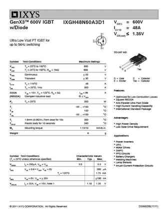
VCES = 600V GenX3TM 600V IGBT IXGH48N60A3D1 w/Diode IC110 = 48A VCE(sat) 1.35V Ultra Low Vsat PT IGBT for up to 5kHz switching TO-247 AD Symbol Test Conditions Maximum Ratings VCES TC = 25 C to 150 C 600 V G C Tab VCGR TJ = 25 C to 150 C, RGE = 1M 600 V E VGES Continuous 20 V VGEM Transient 30 V G = Gate C = Collector E = Emitter Tab = Colle
ixgt28n60b.pdf
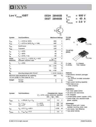
Low VCE(sat) IGBT IXGH 28N60B VCES = 600 V IXGT 28N60B IC25 = 40 A VCE(sat) = 2.0 V Symbol Test Conditions Maximum Ratings TO-268 (IXGT) VCES TJ = 25 C to 150 C 600 V G VCGR TJ = 25 C to 150 C; RGE = 1 M 600 V C (TAB) E VGES Continuous 20 V VGEM Transient 30 V TO-247 AD IC25 TC = 25 C40 A (IXGH) IC90 TC = 90 C28 A ICM TC = 25 C, 1 ms 80 A C (TAB) SSOA VGE = 15 V,
ixgh38n60.pdf
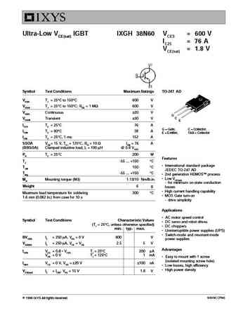
Ultra-Low VCE(sat) IGBT IXGH 38N60 VCES = 600 V IC25 = 76 A VCE(sat) = 1.8 V Symbol Test Conditions Maximum Ratings TO-247 AD VCES TJ = 25 C to 150 C 600 V VCGR TJ = 25 C to 150 C; RGE = 1 M 600 V VGES Continuous 20 V G C VGEM Transient 30 V E IC25 TC = 25 C76 A G = Gate, C = Collector, IC90 TC = 90 C38 A E = Emitter, TAB = Collector ICM TC = 25 C, 1 ms 152 A SSOA
ixgh48n60b3.pdf
IXGA48N60B3 VCES = 600V GenX3TM 600V IGBT IXGP48N60B3 IC110 = 48A IXGH48N60B3 VCE(sat) 1.8V Medium speed low Vsat PT IGBTs 5-40 kHz switching TO-263 (IXGA) Symbol Test Conditions Maximum Ratings G E VCES TC = 25 C to 150 C 600 V (TAB) VCGR TJ = 25 C to 150 C, RGE = 1M 600 V TO-220 (IXGP) VGES Continuous 20 V VGEM Transient 30 V IC110 TC = 1
ixgh28n60b3d1.pdf
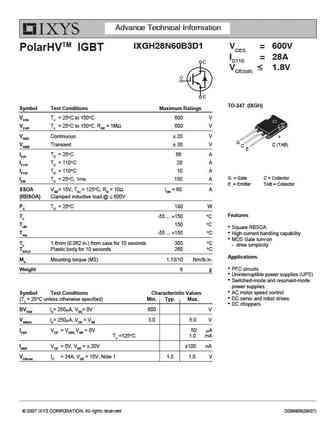
Advance Technical Information IXGH28N60B3D1 VCES = 600V PolarHVTM IGBT IC110 = 28A VCE(sat) 1.8V TO-247 (IXGH) Symbol Test Conditions Maximum Ratings VCES TJ = 25 C to 150 C 600 V VCGR TJ = 25 C to 150 C, RGE = 1M 600 V VGES Continuous 20 V G VGEM Transient 30 V C (TAB) C E IC25 TC = 25 C 66 A IC110 TC = 110 C 28 A IF110 TC = 110 C 10 A
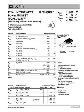
ixfr48n60p.pdf
IXFR 48N60P VDSS = 600 V PolarHVTM HiPerFET ID25 = 32 A Power MOSFET RDS(on) 150 m ISOPLUS247TM trr 200 ns (Electrically Isolated Back Surface) N-Channel Enhancement Mode Avalanche Rated Fast Intrinsic Diode Symbol Test Conditions Maximum Ratings ISOPLUS247 (IXFR) VDSS TJ = 25 C to 150 C 600 V E153432 VDGR TJ
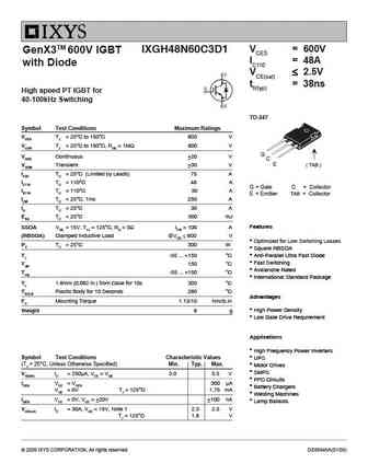
ixgh48n60c3d1.pdf
VCES = 600V IXGH48N60C3D1 GenX3TM 600V IGBT IC110 = 48A with Diode VCE(sat) 2.5V tfi(typ) = 38ns High speed PT IGBT for 40-100kHz Switching TO-247 Symbol Test Conditions Maximum Ratings VCES TJ = 25 C to 150 C 600 V VCGR TJ = 25 C to 150 C, RGE = 1M 600 V G VGES Continuous 20 V C E VGEM Transient 30 V ( TAB ) IC25 TC = 25 C (Limited by Leads)
ixga48n60a3.pdf
IXGA48N60A3 VCES = 600V GenX3TM 600V IXGP48N60A3 IGBTs IC110 = 48A IXGH48N60A3 VCE(sat) 1.35V Ultra Low Vsat PT IGBTs for TO-263 (IXGA) up to 5kHz switching G E Symbol Test Conditions Maximum Ratings C (Tab) VCES TJ = 25 C to 150 C 600 V TO-220 (IXGP) VCGR TJ = 25 C to 150 C, RGE = 1M 600 V VGES Continuous 20 V VGEM Transient 30 V G IC25 TC =
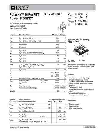
ixfn48n60p.pdf
IXFN 48N60P VDSS = 600 V PolarHVTM HiPerFET ID25 = 40 A Power MOSFET RDS(on) 140 m N-Channel Enhancement Mode trr 200 ns Avalanche Rated Fast Intrinsic Diode Symbol Test Conditions Maximum Ratings VDSS TJ = 25 C to 150 C 600 V miniBLOC, SOT-227 B (IXFN) VDGR TJ = 25 C to 150 C; RGS = 1 M 600 V E153432 S VGSS Cont
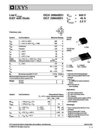
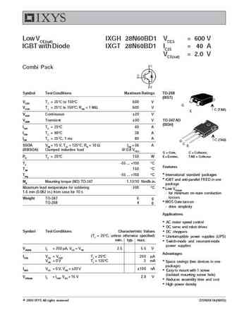
ixgh28n60bd1 ixgt28n60bd1.pdf
Low VCE(sat) IXGH 28N60BD1 VCES = 600 V IGBT with Diode IXGT 28N60BD1 IC25 = 40 A VCE(sat) = 2.0 V Preliminary data Symbol Test Conditions Maximum Ratings TO-268 (IXGT) VCES TJ = 25 C to 150 C 600 V G VCGR TJ = 25 C to 150 C; RGE = 1 MW 600 V E VGES Continuous 20 V C (TAB) VGEM Transient 30 V TO-247 AD (IXGH) IC25 TC = 25 C40 A IC90 TC = 90 C28 A ICM TC = 25 C, 1 ms 8
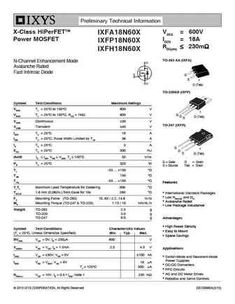
ixfa18n60x ixfh18n60x ixfp18n60x.pdf
Preliminary Technical Information X-Class HiPerFETTM VDSS = 600V IXFA18N60X Power MOSFET ID25 = 18A IXFP18N60X RDS(on) 230m IXFH18N60X TO-263 AA (IXFA) N-Channel Enhancement Mode Avalanche Rated Fast Intrinsic Diode G S D (Tab) TO-220AB (IXFP) Symbol Test Conditions Maximum Ratings VDSS TJ = 25 C to 150 C 600 V VDGR TJ = 25 C to
ixgt28n60bd1.pdf
Low VCE(sat) IXGH 28N60BD1 VCES = 600 V IGBT with Diode IXGT 28N60BD1 IC25 = 40 A VCE(sat) = 2.0 V Combi Pack Symbol Test Conditions Maximum Ratings TO-268 (IXGT) VCES TJ = 25 C to 150 C 600 V G VCGR TJ = 25 C to 150 C; RGE = 1 M 600 V C (TAB) E VGES Continuous 20 V VGEM Transient 30 V TO-247 AD (IXGH) IC25 TC = 25 C40 A IC90 TC = 90 C28 A ICM TC = 25 C, 1 ms 80 A
ixgr48n60b3.pdf
Preliminary Technical Information VCES = 600V GenX3TM 600V IGBTs IXGR48N60B3 IC25 = 60A IXGR48N60B3D1 (Electrically Isolated Back VCE(sat) 2.1V Surface) tfi(typ) = 116ns Medium-Speed Low-Vsat PT IGBTs 5-40 kHz Switching ISOPLUS247TM IXGR_B3 IXGR_B3D1 E153432 Symbol Test Conditions Maximum Ratings VCES TC = 25 C to 150 C 600 V VCGR TJ = 25 C to 150
ixgh28n60bd1.pdf
Low VCE(sat) IXGH 28N60BD1 VCES = 600 V IGBT with Diode IXGT 28N60BD1 IC25 = 40 A VCE(sat) = 2.0 V Combi Pack Symbol Test Conditions Maximum Ratings TO-268 (IXGT) VCES TJ = 25 C to 150 C 600 V G VCGR TJ = 25 C to 150 C; RGE = 1 M 600 V C (TAB) E VGES Continuous 20 V VGEM Transient 30 V TO-247 AD (IXGH) IC25 TC = 25 C40 A IC90 TC = 90 C28 A ICM TC = 25 C, 1 ms 80 A
ixgh48n60c3.pdf
GenX3TM 600V IGBTs IXGI48N60C3 VCES = 600V IXGA48N60C3 IC110 = 48A IXGP48N60C3 2.5V High-Speed PT IGBTs for VCE(sat) 40-100kHz Switching IXGH48N60C3 tfi(typ) = 38ns Symbol Test Conditions Maximum Ratings VCES TC = 25 C to 150 C 600 V VCGR TJ = 25 C to 150 C, RGE = 1M 600 V Features VGES Continuous 20 V Optimized for Low Switching Losses VGEM Tra
ixgh48n60a3.pdf
IXGA48N60A3 VCES = 600V GenX3TM 600V IXGP48N60A3 IGBTs IC110 = 48A IXGH48N60A3 VCE(sat) 1.35V Ultra Low Vsat PT IGBTs for TO-263 (IXGA) up to 5kHz switching G E Symbol Test Conditions Maximum Ratings C (Tab) VCES TJ = 25 C to 150 C 600 V TO-220 (IXGP) VCGR TJ = 25 C to 150 C, RGE = 1M 600 V VGES Continuous 20 V VGEM Transient 30 V G IC25 TC =
ixfq28n60p3 ixfh28n60p3.pdf
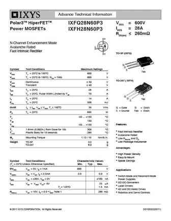
Advance Technical Information Polar3TM HiperFETTM VDSS = 600V IXFQ28N60P3 ID25 = 28A Power MOSFETs IXFH28N60P3 RDS(on) 260m N-Channel Enhancement Mode Avalanche Rated Fast Intrinsic Rectifier TO-3P (IXFQ) G D Symbol Test Conditions Maximum Ratings S Tab VDSS TJ = 25 C to 150 C 600 V VDGR TJ = 25 C to 150 C, RGS = 1M 600 V TO-247 ( IX
ixfk48n60p ixfx48n60p.pdf
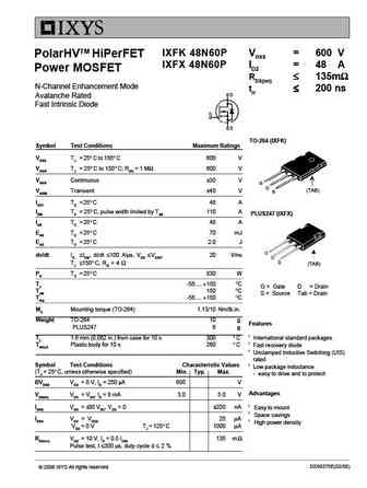
IXFK 48N60P VDSS = 600 V PolarHVTM HiPerFET IXFX 48N60P ID2 = 48 A Power MOSFET RDS(on) 135m N-Channel Enhancement Mode trr 200 ns Avalanche Rated Fast Intrinsic Diode TO-264 (IXFK) Symbol Test Conditions Maximum Ratings VDSS TJ = 25 C to 150 C 600 V VDGR TJ = 25 C to 150 C; RGS = 1 M 600 V VGSS Continuou
ixgh28n60b.pdf
Low VCE(sat) IGBT IXGH 28N60B VCES = 600 V IXGT 28N60B IC25 = 40 A VCE(sat) = 2.0 V Symbol Test Conditions Maximum Ratings TO-268 (IXGT) VCES TJ = 25 C to 150 C 600 V G VCGR TJ = 25 C to 150 C; RGE = 1 M 600 V C (TAB) E VGES Continuous 20 V VGEM Transient 30 V TO-247 AD IC25 TC = 25 C40 A (IXGH) IC90 TC = 90 C28 A ICM TC = 25 C, 1 ms 80 A C (TAB) SSOA VGE = 15 V,
ixgp48n60c3.pdf
GenX3TM 600V IGBTs IXGI48N60C3 VCES = 600V IXGA48N60C3 IC110 = 48A IXGP48N60C3 2.5V High-Speed PT IGBTs for VCE(sat) 40-100kHz Switching IXGH48N60C3 tfi(typ) = 38ns Symbol Test Conditions Maximum Ratings VCES TC = 25 C to 150 C 600 V VCGR TJ = 25 C to 150 C, RGE = 1M 600 V Features VGES Continuous 20 V Optimized for Low Switching Losses VGEM Tra
ixgh48n60b3c1.pdf
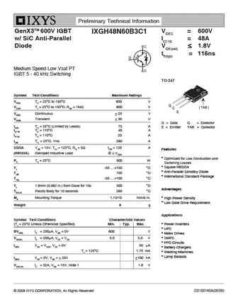
Preliminary Technical Information GenX3TM 600V IGBT VCES = 600V IXGH48N60B3C1 w/ SiC Anti-Parallel IC110 = 48A Diode VCE(sat) 1.8V tfi(typ) = 116ns Medium Speed Low Vsat PT IGBT 5 - 40 kHz Switching TO-247 Symbol Test Conditions Maximum Ratings VCES TC = 25 C to 150 C 600 V G VCGR TJ = 25 C to 150 C, RGE = 1M 600 V ( TAB ) C E VGES Continuous 20
ixgi48n60c3.pdf
GenX3TM 600V IGBTs IXGI48N60C3 VCES = 600V IXGA48N60C3 IC110 = 48A IXGP48N60C3 2.5V High-Speed PT IGBTs for VCE(sat) 40-100kHz Switching IXGH48N60C3 tfi(typ) = 38ns Symbol Test Conditions Maximum Ratings VCES TC = 25 C to 150 C 600 V VCGR TJ = 25 C to 150 C, RGE = 1M 600 V Features VGES Continuous 20 V Optimized for Low Switching Losses VGEM Tra
ixgh48n60b3d1.pdf
Preliminary Technical Information VCES = 600V GenX3TM 600V IGBT IXGH48N60B3D1 with Diode IC110 = 48A VCE(sat) 1.8V Medium speed low Vsat PT IGBTs 5-40 kHz switching TO-247(IXGH) Symbol Test Conditions Maximum Ratings VCES TC = 25 C to 150 C 600 V VCGR TJ = 25 C to 150 C, RGE = 1M 600 V VGES Continuous 20 V VGEM Transient 30 V G ( TAB ) C E I
ixgh48n60c3c1.pdf
Preliminary Technical Information GenX3TM 600V IGBT VCES = 600V IXGH48N60C3C1 w/ SiC Anti-Parallel IC110 = 48A Diode VCE(sat) 2.5V tfi(typ) = 38ns High Speed PT IGBT for 40 - 100kHz Switching TO-247 Symbol Test Conditions Maximum Ratings VCES TJ = 25 C to 150 C 600 V VCGR TJ = 25 C to 150 C, RGE = 1M 600 V G C VGES Continuous 20 V E ( TAB ) VGEM
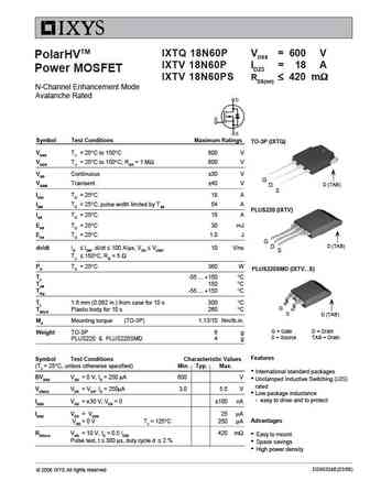
ixfh18n60p ixfv18n60p.pdf
IXFH 18N60P VDSS = 600 V PolarHVTM HiPerFET IXFV 18N60P ID25 = 18 A Power MOSFET IXFV 18N60PS RDS(on) 400 m N-Channel Enhancement Mode trr 200 ns Fast Intrinsic Diode Avalanche Rated Symbol Test Conditions Maximum Ratings TO-247 AD (IXFH) VDSS TJ = 25 C to 150 C 600 V VDGR TJ = 25 C to 150 C; RGS = 1 M 600 V VGS Co
ixga48n60b3.pdf
IXGA48N60B3 VCES = 600V GenX3TM 600V IGBT IXGP48N60B3 IC110 = 48A IXGH48N60B3 VCE(sat) 1.8V Medium speed low Vsat PT IGBTs 5-40 kHz switching TO-263 (IXGA) Symbol Test Conditions Maximum Ratings G E VCES TC = 25 C to 150 C 600 V (TAB) VCGR TJ = 25 C to 150 C, RGE = 1M 600 V TO-220 (IXGP) VGES Continuous 20 V VGEM Transient 30 V IC110 TC = 1
ixgp48n60a3.pdf
IXGA48N60A3 VCES = 600V GenX3TM 600V IXGP48N60A3 IGBTs IC110 = 48A IXGH48N60A3 VCE(sat) 1.35V Ultra Low Vsat PT IGBTs for TO-263 (IXGA) up to 5kHz switching G E Symbol Test Conditions Maximum Ratings C (Tab) VCES TJ = 25 C to 150 C 600 V TO-220 (IXGP) VCGR TJ = 25 C to 150 C, RGE = 1M 600 V VGES Continuous 20 V VGEM Transient 30 V G IC25 TC =
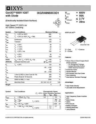
ixgr48n60c3d1.pdf
GenX3TM 600V IGBT VCES = 600V IXGR48N60C3D1 with Diode IC25 = 56A VCE(sat) 2.7V (Electrically Isolated Back Surface) tfi(typ) = 38ns High Speed PT IGBTs for 40-100kHz Switching Symbol Test Conditions Maximum Ratings ISOPLUS 247TM VCES TJ = 25 C to 150 C 600 V VCGR TJ = 25 C to 150 C, RGE = 1M 600 V VGES Continuous 20 V VGEM Transient 30 V G C IC
fdpf8n60zut.pdf
Is Now Part of To learn more about ON Semiconductor, please visit our website at www.onsemi.com Please note As part of the Fairchild Semiconductor integration, some of the Fairchild orderable part numbers will need to change in order to meet ON Semiconductor s system requirements. Since the ON Semiconductor product management systems do not have the ability to manage part nomenclatur
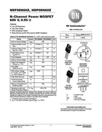
ndf08n60z-d.pdf
NDF08N60Z, NDP08N60Z N-Channel Power MOSFET 600 V, 0.95 W Features Low ON Resistance Low Gate Charge http //onsemi.com 100% Avalanche Tested These Devices are Pb-Free and are RoHS Compliant VDSS RDS(ON) (MAX) @ 3.5 A ABSOLUTE MAXIMUM RATINGS (TC = 25 C unless otherwise noted) 600 V 0.95 W Rating Symbol NDF08N60Z NDP08N60Z Unit Drain-to-Source Voltage VDSS 600 V N
fqp8n60c fqpf8n60c.pdf
QFET FQP8N60C/FQPF8N60C 600V N-Channel MOSFET General Description Features These N-Channel enhancement mode power field effect 7.5A, 600V, RDS(on) = 1.2 @VGS = 10 V transistors are produced using Fairchild s proprietary, Low gate charge ( typical 28 nC) planar stripe, DMOS technology. Low Crss ( typical 12 pF) This advanced technology has been especially tailored to
fqb8n60c fqi8n60c.pdf
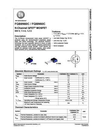
FQB8N60C / FQI8N60C N-Channel QFET MOSFET 600 V, 7.5 A, 1.2 Features 7.5 A, 600 V, RDS(on) = 1.2 (Max.) @ VGS = 10 V, ID = 3.75 A Description Low Gate Charge (Typ. 28 nC) This N-Channel enhancement mode power MOSFET is produced using ON Semiconductor s proprietary planar Low Crss (Typ. 12 pF) stripe and DMOS technology. This advanced MOSFET technology has
fqpf8n60cf.pdf
Is Now Part of To learn more about ON Semiconductor, please visit our website at www.onsemi.com Please note As part of the Fairchild Semiconductor integration, some of the Fairchild orderable part numbers will need to change in order to meet ON Semiconductor s system requirements. Since the ON Semiconductor product management systems do not have the ability to manage part nomenclatur
8n60kl-ta3-t 8n60kg-ta3-t 8n60kl-tf1-t 8n60kg-tf1-t 8n60kl-tf2-t 8n60kg-tf2-t 8n60kl-tf3-t 8n60kg-tf3-t 8n60kl-tf3t-t 8n60kg-tf3t-t.pdf
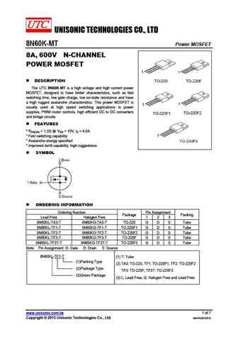
UNISONIC TECHNOLOGIES CO., LTD 8N60K-MT Power MOSFET 8A, 600V N-CHANNEL POWER MOSFET DESCRIPTION The UTC 8N60K-MT is a high voltage and high current power MOSFET, designed to have better characteristics, such as fast switching time, low gate charge, low on-state resistance and have a high rugged avalanche characteristics. This power MOSFET is usually used at high speed swi
8n60l-ta3-t 8n60g-ta3-t 8n60l-tf1-t 8n60g-tf1-t 8n60l-tf2-t 8n60g-tf2-t 8n60l-tf3-t 8n60g-tf3-t 8n60l-t2q-t 8n60g-t2q-t.pdf
UNISONIC TECHNOLOGIES CO., LTD 8N60 Power MOSFET 8A, 600V N-CHANNEL POWER MOSFET DESCRIPTION The UTC 8N60 is a high voltage and high current power MOSFET, designed to have better characteristics, such as fast switching time, low gate charge, low on-state resistance and have a high rugged avalanche characteristics. This power MOSFET is usually used at high speed switching app
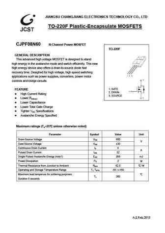
cjpf08n60.pdf
JIANGSU CHANGJIANG ELECTRONICS TECHNOLOGY CO., LTD TO-220F Plastic-Encapsulate MOSFETS CJPF08N60 N-Channel Power MOSFET TO-220F GENERAL DESCRIPTION This advanced high voltage MOSFET is designed to stand high energy in the avalanche mode and switch efficiently. This new high energy device also offers a drain-to-source diode fast recovery time. Desighed for high voltage, high s
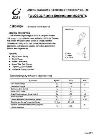
cjp08n60.pdf
JIANGSU CHANGJIANG ELECTRONICS TECHNOLOGY CO., LTD TO-220-3L Plastic-Encapsulate MOSFETS CJP08N60 N-Channel Power MOSFET TO-220-3L GENERAL DESCRIPTION This advanced high voltage MOSFET is designed to stand high energy in the avalanche mode and switch efficiently. This new high energy device also offers a drain-to-source diode fast recovery time. Desighed for high voltage, hig
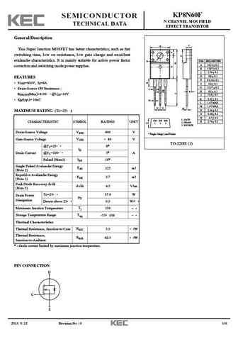
kp8n60f.pdf
KP8N60F SEMICONDUCTOR N CHANNEL MOS FIELD TECHNICAL DATA EFFECT TRANSISTOR General Description C A This Super Junction MOSFET has better characteristics, such as fast switching time, low on resistance, low gate charge and excellent avalanche characteristics. It is mainly suitable for active power factor E DIM MILLIMETERS _ A 10.16 0.2 + correction and switching mode power suppli
kp8n60d.pdf
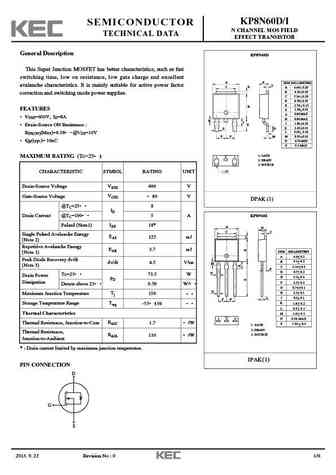
KP8N60D/I SEMICONDUCTOR N CHANNEL MOS FIELD TECHNICAL DATA EFFECT TRANSISTOR General Description KP8N60D This Super Junction MOSFET has better characteristics, such as fast switching time, low on resistance, low gate charge and excellent A K DIM MILLIMETERS L avalanche characteristics. It is mainly suitable for active power factor C D _ A 6.60 + 0.20 _ B 6.10 + 0.20 correctio
kf8n60p-f.pdf
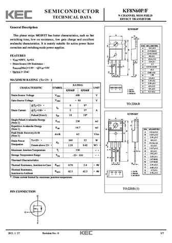
KF8N60P/F SEMICONDUCTOR N CHANNEL MOS FIELD TECHNICAL DATA EFFECT TRANSISTOR General Description KF8N60P A This planar stripe MOSFET has better characteristics, such as fast O C switching time, low on resistance, low gate charge and excellent F avalanche characteristics. It is mainly suitable for active power factor E DIM MILLIMETERS G correction and switching mode power suppli
apt38n60bc6 apt38n60sc6.pdf
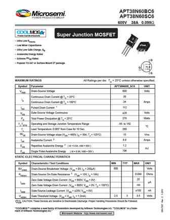
APT38N60BC6 APT38N60SC6 600V 38A 0.099 COOLMOS Power Semiconductors Super Junction MOSFET Ultra Low RDS(ON) D3PAK Low Miller Capacitance Ultra Low Gate Charge, Qg Avalanche Energy Rated Extreme dv/dt Rated D Popular TO-247 or Surface Mount D3 package. G S MAXIMUM RATINGS All Ratings per die TC = 25 C unless otherwise specified. Symbol Parame
8n60p 8n60f.pdf
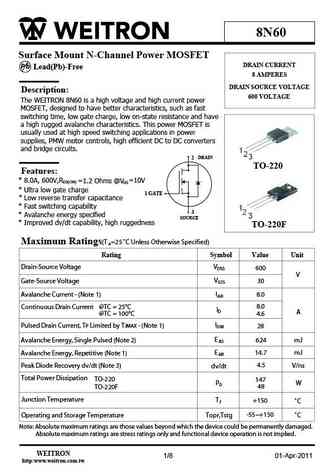
8N60 Surface Mount N-Channel Power MOSFET DRAIN CURRENT P b Lead(Pb)-Free 8 AMPERES DRAIN SOURCE VOLTAGE Description 600 VOLTAGE The WEITRON 8N60 is a high voltage and high current power MOSFET, designed to have better characteristics, such as fast switching time, low gate charge, low on-state resistance and have a high rugged avalanche characteristics. This power MOSFET is usually
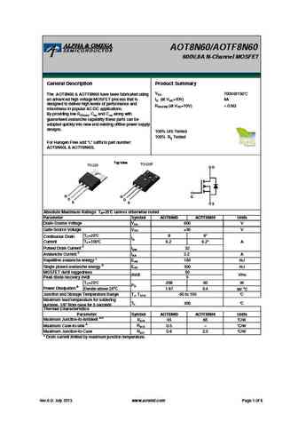
aotf8n60.pdf
AOT8N60/AOTF8N60 600V,8A N-Channel MOSFET General Description Product Summary VDS 700V@150 The AOT8N60 & AOTF8N60 have been fabricated using an advanced high voltage MOSFET process that is ID (at VGS=10V) 8A designed to deliver high levels of performance and RDS(ON) (at VGS=10V)
aot8n60.pdf
AOT8N60/AOTF8N60 600V,8A N-Channel MOSFET General Description Product Summary VDS 700V@150 The AOT8N60 & AOTF8N60 have been fabricated using an advanced high voltage MOSFET process that is ID (at VGS=10V) 8A designed to deliver high levels of performance and RDS(ON) (at VGS=10V)
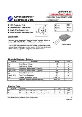
ap08n60i-hf.pdf
AP08N60I-HF Halogen-Free Product Advanced Power N-CHANNEL ENHANCEMENT MODE Electronics Corp. POWER MOSFET 100% Avalanche Test BVDSS 600V D Fast Switching Characteristic RDS(ON) 0.85 Simple Drive Requirement ID 8A G RoHS Compliant & Halogen-Free S Description AP08N60 series are specially designed as main switching devices for universal 90 265VAC off-line AC/DC conv
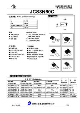
jcs8n60vc jcs8n60rc jcs8n60bc jcs8n60sc jcs8n60cc jcs8n60fc.pdf
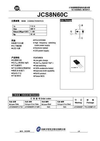
N R N-CHANNEL MOSFET JCS8N60C Package MAIN CHARACTERISTICS ID 7.0 A VDSS 600 V Rdson 1.6 @Vgs=10V Qg 32 nC APPLICATIONS High frequency switching mode power supply Electronic ballast LED LED power supply FEATU
jcs8n60bb jcs8n60sb jcs8n60cb jcs8n60fb.pdf
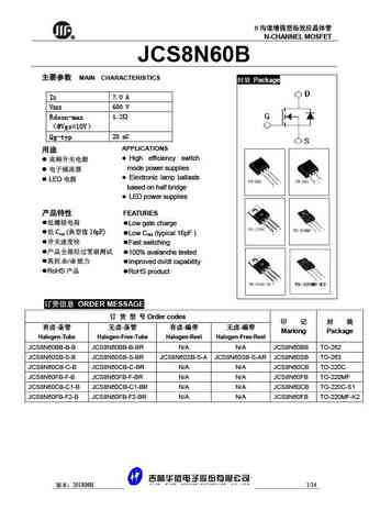
N R N-CHANNEL MOSFET JCS8N60B MAIN CHARACTERISTICS Package ID 7.0 A VDSS 600 V Rdson-max 1.2 @Vgs=10V Qg-typ 25 nC APPLICATIONS High efficiency switch mode power supplies Electronic lamp ballasts LED based on half bridge L
mtn8n60e3.pdf
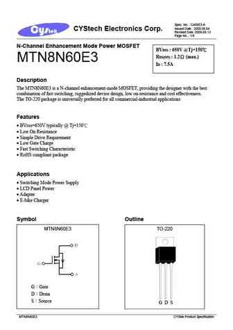
Spec. No. C409E3-A Issued Date 2009.08.04 CYStech Electronics Corp. Revised Date 2009.08.13 Page No. 1/8 N-Channel Enhancement Mode Power MOSFET BVDSS 650V @Tj=150 RDS(ON) 1.2 (max.) MTN8N60E3 ID 7.5A Description The MTN8N60E3 is a N-channel enhancement-mode MOSFET, providing the designer with the best combination of fast switching, ruggedized device des
mtn8n60fp.pdf
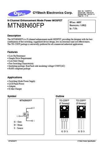
Spec. No. C409FP-A Issued Date 2009.04.29 CYStech Electronics Corp. Revised Date 2012.01.13 Page No. 1/ 10 N-Channel Enhancement Mode Power MOSFET BVDSS 600V RDSON(TYP) 1.08 MTN8N60FP ID 7.5A Description The MTN8N60FP is a N-channel enhancement-mode MOSFET, providing the designer with the best combination of fast switching, ruggedized device design, low on
8n60a.pdf
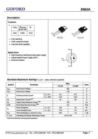
GOFORD 8N60A Description Features VDSS RDS(ON) ID @ 10V (typ) 8.5A 600V 0.94 Fast switching 100% avalanche tested Improved dv/dt capability Application High frequency switching mode power supply Uninterruptible Power Supply (UPS) Electronic ballast Absolute Maximum Ratings TC=25 unless otherwise specified Max. Symbol Parameter Un
sdf08n60 sdp08n60.pdf
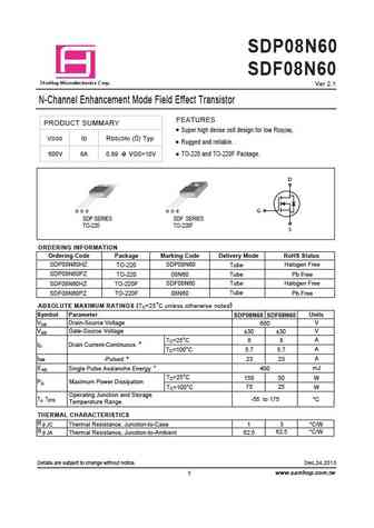
SDP08N60 SDF08N60 a S mHop Microelectronics C orp. Ver 2.1 N-Channel Enhancement Mode Field Effect Transistor FEATURES PRODUCT SUMMARY Super high dense cell design for low RDS(ON). RDS(ON) ( ) Typ VDSS ID Rugged and reliable. 600V 8A 0.89 @ VGS=10V TO-220 and TO-220F Package. D G D S G D S G SDP SERIES SDF SERIES TO-220 TO-220F S ORDERING INFORMATION Ordering Code Package Ma
ssf8n60.pdf
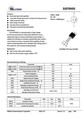
SSF8N60 Features VDSS = 600V Extremely high dv/dt capability ID = 8A Low Gate Charge Qg results in Simple Drive Requirement Rdson = 0.85 (typ.) 100% avalanche tested Gate charge minimized Very low intrinsic capacitances Very good manufacturing repeatability Description The SSF8N60 is a new generation of high voltage N Channel enhancement mod
brf8n60.pdf
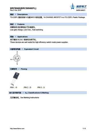
BRF8N60(BRCS8N60FL) Rev.C Feb.-2015 DATA SHEET / Descriptions TO-220FL N MOS N-CHANNEL MOSFET in a TO-220FL Plastic Package. / Features , , Low gate charge, Low Crss , Fast switching. / Applications DC/DC These devices are well suited for h
brfl8n60.pdf
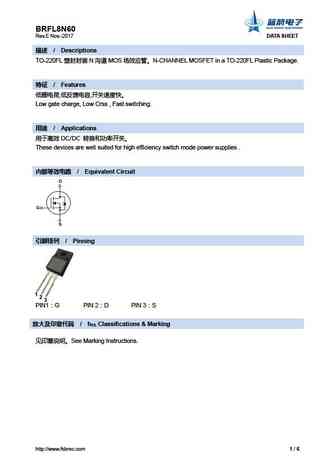
BRFL8N60 Rev.E Nov.-2017 DATA SHEET / Descriptions TO-220FL N MOS N-CHANNEL MOSFET in a TO-220FL Plastic Package. / Features , , Low gate charge, Low Crss , Fast switching. / Applications DC/DC These devices are well suited for high efficie
br8n60.pdf
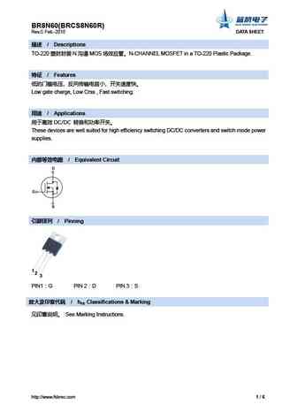
BR8N60(BRCS8N60R) Rev.C Feb.-2015 DATA SHEET / Descriptions TO-220 N MOS N-CHANNEL MOSFET in a TO-220 Plastic Package. / Features Low gate charge, Low Crss , Fast switching. / Applications DC/DC These devices are well su
8n60h.pdf
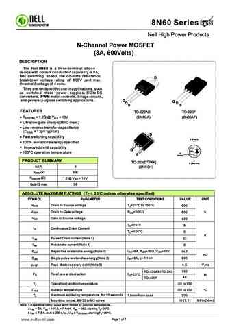
RoHS 8N60 Series RoHS SEMICONDUCTOR Nell High Power Products N-Channel Power MOSFET (8A, 600Volts) DESCRIPTION The Nell 8N60 is a three-terminal silicon device with current conduction capability of 8A, fast switching speed, low on-state resistance, D breakdown voltage rating of 600V ,and max. threshold voltage of 4 volts. They are designed for use in applications. such as sw
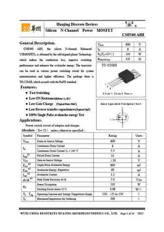
cs8n60 a8h.pdf
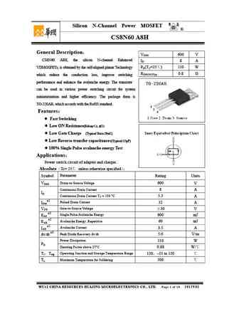
Silicon N-Channel Power MOSFET R CS8N60 A8H General Description VDSS 600 V CS8N60 A8H, the silicon N-channel Enhanced ID 8 A PD(TC=25 ) 110 W VDMOSFETs, is obtained by the self-aligned planar Technology RDS(ON)Typ 0.8 which reduce the conduction loss, improve switching performance and enhance the avalanche energy. The transistor can be used in various power
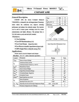
cs8n60f a9h.pdf
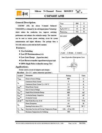
Silicon N-Channel Power MOSFET R CS8N60F A9H General Description VDSS 600 V CS8N60F A9H, the silicon N-channel Enhanced ID 8 A PD(TC=25 ) 45 W VDMOSFETs, is obtained by the self-aligned planar Technology RDS(ON)Typ 0.8 which reduce the conduction loss, improve switching performance and enhance the avalanche energy. The transistor can be used in various powe
cs8n60 ard.pdf
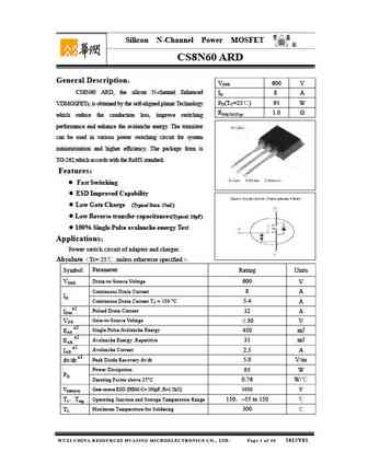
Silicon N-Channel Power MOSFET R CS8N60 ARD General Description VDSS 600 V CS8N60 ARD, the silicon N-channel Enhanced ID 8 A PD(TC=25 ) 95 W VDMOSFETs, is obtained by the self-aligned planar Technology RDS(ON)Typ 1.0 which reduce the conduction loss, improve switching performance and enhance the avalanche energy. The transistor can be used in various power
cs8n60 a8d.pdf
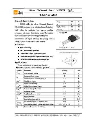
Silicon N-Channel Power MOSFET R CS8N60 A8D General Description VDSS 600 V CS8N60 A8D, the silicon N-channel Enhanced ID 8 A PD(TC=25 ) 95 W VDMOSFETs, is obtained by the self-aligned planar Technology RDS(ON)Typ 1.0 which reduce the conduction loss, improve switching performance and enhance the avalanche energy. The transistor can be used in various power s
cm8n60f.pdf
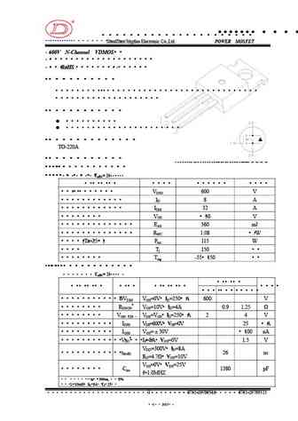
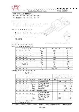
R CM8N60F www.jdsemi.cn ShenZhen Jingdao Electronic Co.,Ltd. POWER MOSFET 600V N-Channel VDMOS RoHS 1 LD E 2 1
f8n60.pdf
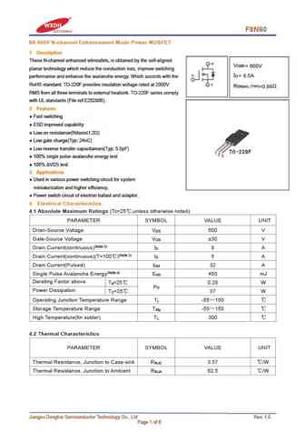
F8N60 8A 600V N-channel Enhancement Mode Power MOSFET 1 Description These N-channel enhanced vdmosfets, is obtained by the self-aligned V DSS = 600V planar technology which reduce the conduction loss, improve switching I = 8.0A D performance and enhance the avalanche energy. Which accords with the RoHS standard. TO-220F provides insulation voltage rated at 2000V R DS(on) TYP) =0.
kx8n60cf.pdf
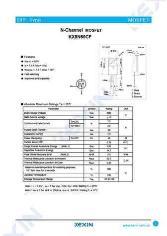
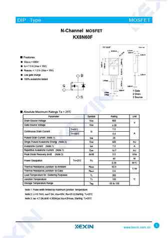
DIP Type MOSFET N-Channel MOSFET KX8N60CF Unit mm TO-220F 0.20 0.20 0.20 2.54 0.20 0.70 Features VDS (V) = 600V ID = 7.5 A (VGS = 10V) RDS(ON) 1.2 (VGS = 10V) D 0.20 Fast switching 2.76 Improved dv/dt capability 1.47max 0.20 0.50 1 2 3 G 0.20 0.80 2.54typ S 2.54typ Absolute Maximum Ratings Ta = 25 Parameter
kx8n60c.pdf
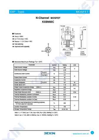
DIP Type MOSFET N-Channel MOSFET KX8N60C TO-220 9.90 0.20 4.50 0.20 (8.70) +0.10 3.60 0.10 1.30 0.05 Features VDS (V) = 600V ID = 7.5 A (VGS = 10V) RDS(ON) 1.2 (VGS = 10V) D Fast switching 1.27 0.10 1.52 0.10 2 1 3 Improved dv/dt capability 0.80 0.10 +0.10 0.50 0.05 2.40 0.20 2.54TYP 2.54TYP [2.54 0.20 ] [2.
kx8n60f.pdf
DIP Type MOSFET N-Channel MOSFET KX8N60F Unit mm TO-220F 0.20 0.20 0.20 2.54 0.20 0.70 Features VDS (V) = 600V ID = 7.5 A (VGS = 10V) RDS(ON) 1.2 (VGS = 10V) 0.20 2.76 Low gate charge 100% avalanche tested 1.47max 0.20 0.50 0.20 0.80 2.54typ 2.54typ Absolute Maximum Ratings Ta = 25 Parameter Symbol Rating Unit
svf8n60t svf8n60f.pdf
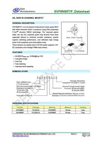
SVF8N60T/F_Datasheet 8A, 600V N-CHANNEL MOSFET GENERAL DESCRIPTION SVF8N60T/F is an N-channel enhancement mode power MOS field effect transistor which is produced using Silan proprietary F-CellTM structure DMOS technology. The improved planar stripe cell and the improved guard ring terminal have been especially tailored to minimize on-state resistance, provide superior switching
mdp8n60th.pdf
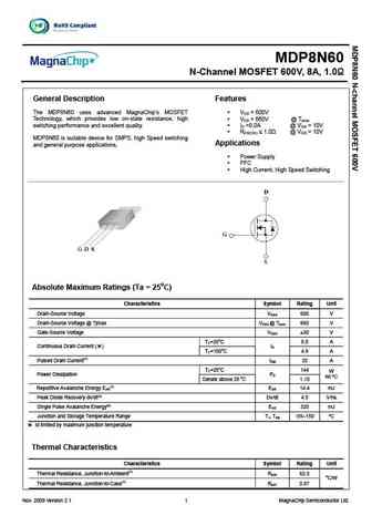
MDP8N60 N-Channel MOSFET 600V, 8A, 1.0 General Description Features The MDP8N60 uses advanced MagnaChip s MOSFET V = 600V DS Technology, which provides low on-state resistance, high V = 660V @ T DS jmax switching performance and excellent quality. I =8.0A @ V = 10V D GS RDS(ON) 1.0 @ VGS = 10V MDP8N60 is suitable device for SMPS, high Speed switching Applicatio
mdf8n60bth.pdf
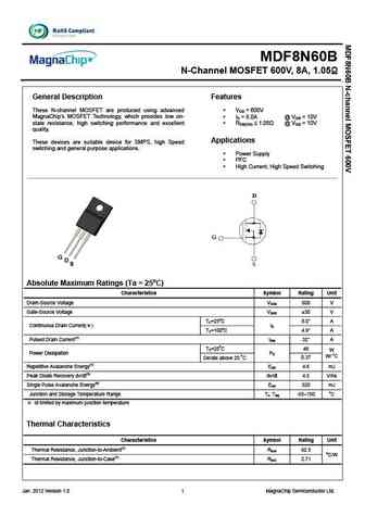
MDF8N60B N-Channel MOSFET 600V, 8A, 1.05 General Description Features These N-channel MOSFET are produced using advanced VDS = 600V MagnaChip s MOSFET Technology, which provides low on- ID = 8.0A @ VGS = 10V state resistance, high switching performance and excellent RDS(ON) 1.05 @ VGS = 10V quality. Applications These devices are suitable device for SMP
ms8n60.pdf
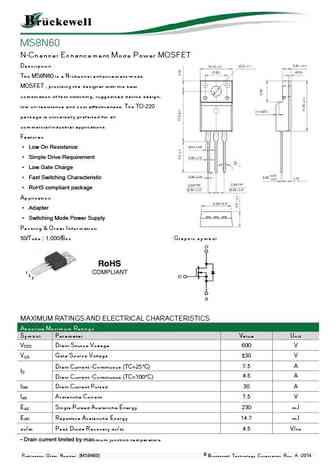
MS8N60 N-Channel Enhancement Mode Power MOSFET Description The MS8N60 is a N-channel enhancement-mode MOSFET , providing the designer with the best combination of fast switching, ruggedized device design, low on-resistance and cost effectiveness. The TO-220 package is universally preferred for all commercial-industrial applications Features Low On Resistance Simple
msf8n60.pdf
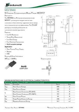
MSF8N60 N-Channel Enhancement Mode Power MOSFET Description The MSF8N60 is a N-channel enhancement-mode MOSFET , providing the designer with the best combination of fast switching, ruggedized device design, low on-resistance and cost effectiveness. The TO-220F package is universally preferred for all commercial-industrial applications Features Low On Resistance Sim
wfp8n60b.pdf
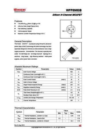
WFP8N60B WFP8N60B WFP8N60B WFP8N60B Silicon N-Channel MOSFET Silicon N-Channel MOSFET Silicon N-Channel MOSFET Silicon N-Channel MOSFET Features 7.5A,600V,R (Max1.2 )@V =10V DS(on) GS Ultra-low Gate charge(Typical 28nC) Fast Switching Capability 100%Avalanche Tested Maximum Junction Temperature Range(150 ) General Description This Power MOSFET is produced
wfp8n60.pdf
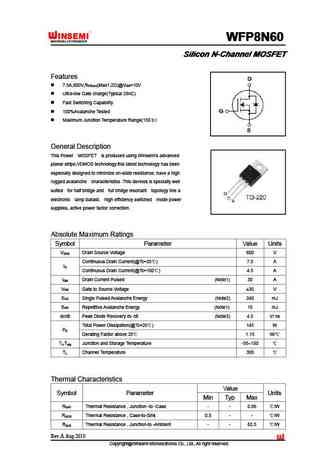
WFP8N60 WFP8N60 WFP8N60 WFP8N60 Silicon N-Channel MOSFET Silicon N-Channel MOSFET Silicon N-Channel MOSFET Silicon N-Channel MOSFET Features 7.5A,600V,R (Max1.2 )@V =10V DS(on) GS Ultra-low Gate charge(Typical 28nC) Fast Switching Capability 100%Avalanche Tested Maximum Junction Temperature Range(150 ) General Description This Power MOSFET is produced usi
wff8n60.pdf
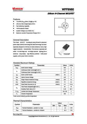
WFF8N60 WFF8N60 WFF8N60 WFF8N60 Silicon N-Channel MOSFET Silicon N-Channel MOSFET Silicon N-Channel MOSFET Silicon N-Channel MOSFET Features 7.5A,600V,R (Max1.2 )@V =10V DS(on) GS Ultra-low Gate charge(Typical 28nC) Fast Switching Capability 100%Avalanche Tested Isolation Voltage (V =4000V AC) ISO Maximum Junction Temperature Range(150 ) General Desc
wff8n60b.pdf
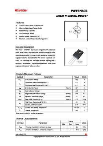
WFF8N60B WFF8N60B WFF8N60B WFF8N60B Silicon N-Channel MOSFET Silicon N-Channel MOSFET Silicon N-Channel MOSFET Silicon N-Channel MOSFET Features 7.5A,600V,R (Max1.2 )@V =10V DS(on) GS Ultra-low Gate charge(Typical 28nC) Fast Switching Capability 100%Avalanche Tested Isolation Voltage (V =4000V AC) ISO Maximum Junction Temperature Range(150 ) General
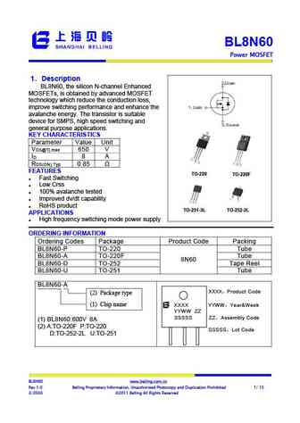
bl8n60-p bl8n60-a bl8n60-d bl8n60-u.pdf
BL8N60 Power MOSFET 1 Description Step-Down Converter BL8N60, the silicon N-channel Enhanced , MOSFETs, is obtained by advanced MOSFET technology which reduce the conduction loss, improve switching performance and enhance the avalanche energy. The transistor is suitable device for SMPS, high speed switching and general purpose applications. KEY CHARACTERISTICS Para
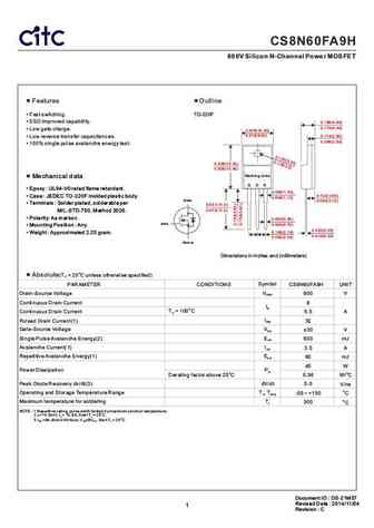
cs8n60fa9h.pdf
CS8N60FA9H 600V Silicon N-Channel Power MOSFET Features Outline Fast switching. TO-220F ESD improved capability. 0.189(4.80) 0.173(4.40) Low gate charge. 0.409(10.40) 0.378(9.60) 0.114(2.90) Low reverse transfer capacitances. 0.098(2.50) 100% single pulse avalanche energy test. 0.638(16.20) 0.606(15.40) Marking code Mechanical data G D S Epo
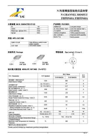
fhp8n60a fhf8n60a.pdf
N N-CHANNEL MOSFET FHP8N60A /FHF8N60A MAIN CHARACTERISTICS FEATURES ID 8A Low gate charge VDSS 600V Crss ( 15pF) Low Crss (typical 15pF ) Rdson-typ @Vgs=10V 0.9 Fast switching Qg-typ 29nC 100% 100% avalanche tested dv/dt Improved dv/dt
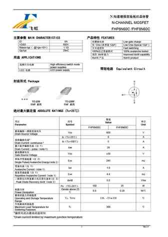
fhp8n60c fhf8n60c.pdf
N N-CHANNEL MOSFET FHP8N60C /FHF8N60C MAIN CHARACTERISTICS FEATURES ID 8A Low gate charge VDSS 600V Crss ( 12pF) Low Crss (typical 12pF ) Rdson-typ @Vgs=10V 1.1 Fast switching Qg-typ 29nC 100% 100% avalanche tested dv/dt Improv
jfpc8n60c jffm8n60c.pdf
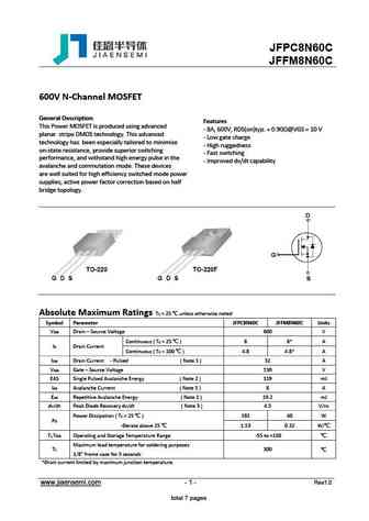
JFPC8N60C JFFM8N60C 600V N-Channel MOSFET General Description Features This Power MOSFET is produced using advanced - 8A, 600V, RDS(on)typ. = 0.90 @VGS = 10 V planar stripe DMOS technology. This advanced - Low gate charge technology has been especially tailored to minimize - High ruggedness on-state resistance, provide superior switching - Fast switching performance,
jfpc18n60ci.pdf
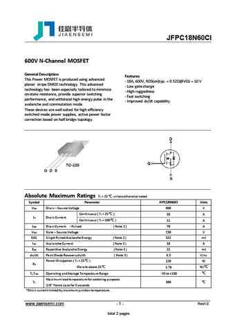
JFPC18N60CI 600V N-Channel MOSFET General Description Features This Power MOSFET is produced using advanced - 18A, 600V, RDS(on)typ. = 0.52 @VGS = 10 V planar stripe DMOS technology. This advanced - Low gate charge technology has been especially tailored to minimize - High ruggedness on-state resistance, provide superior switching - Fast switching performance, and withs
jfpc18n60c jffm18n60c.pdf
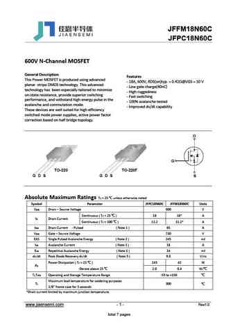
JFFM18N60C JFPC18N60C 600V N-Channel MOSFET General Description Features This Power MOSFET is produced using advanced - 18A, 600V, RDS(on)typ. = 0.42 @VGS = 10 V planar stripe DMOS technology. This advanced - Low gate charge(40nC) technology has been especially tailored to minimize - High ruggedness on-state resistance, provide superior switching - Fast switching perf
kia8n60h.pdf
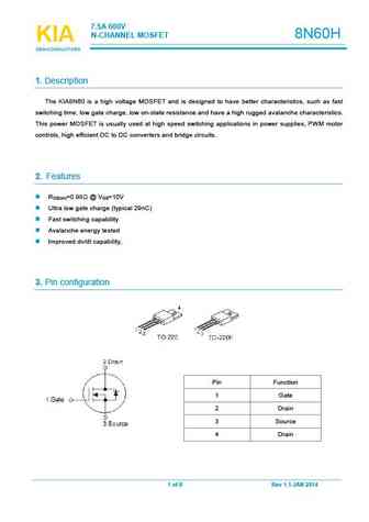
7.5A600V N-CHANNELMOSFET 8N60H KIA KIA KIA SEMICONDUCTORS SEMICONDUCTORS SEMICONDUCTORS 1.Description The KIA8N60 is a high voltage MOSFET and is designed to have better characteristics, such as fast switchingtime, lowgate charge, lowon-state resistanceand have ahigh rugged avalanchecharacteristics. This power MOSFET is usually used at high speed switching applications in power supp
cs8n60f.pdf
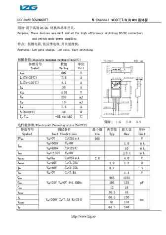
BRF8N60(CS8N60F) N-Channel MOSFET/N MOS DC/DC Purpose These devices are well suited for high efficiency switching DC/DC converters and switch mode power supplies. , , Features Low gate charge, low crss, fast switching. /Absolute maximum ratings(Ta=25 )
slp8n60c slf8n60c.pdf
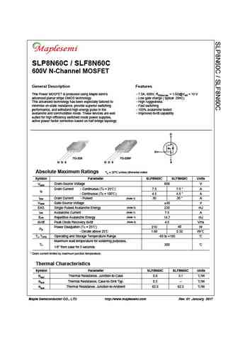
SLP8N60C / SLF8N60C 600V N-Channel MOSFET General Description Features This Power MOSFET is produced using Maple semi s - 7.5A, 600V, RDS(on) typ. = 1.0 @VGS = 10 V advanced planar stripe DMOS technology. - Low gate charge ( typical 29nC) This advanced technology has been especially tailored to - High ruggedness minimize on-state resistance, provide superior switching - Fast switching
ncep018n60agu.pdf
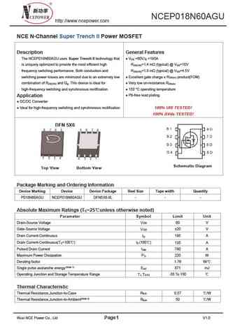
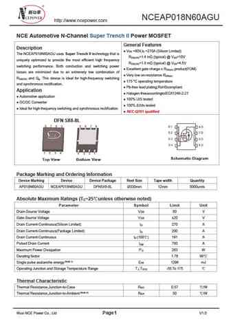
NCEP018N60AGU http //www.ncepower.com NCE N-Channel Super Trench II Power MOSFET Description General Features The NCEP018N60AGU uses Super Trench II technology that V =60V,I =195A DS D is uniquely optimized to provide the most efficient high R =1.4 m (typical) @ V =10V DS(ON) GS frequency switching performance. Both conduction and R =1.8 m (typical) @ V =4.5V DS(ON) GS switchi
nceap018n60gu.pdf
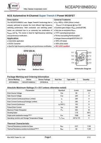
NCEAP018N60GU http //www.ncepower.com NCE Automotive N-Channel Super Trench II Power MOSFET Description General Features The NCEAP018N60GU uses Super Trench II technology that is V =60V,I =256A (Silicon Limited) DS D uniquely optimized to provide the most efficient high frequency R =1.6 m (typical) @ V =10V DS(ON) GS switching performance. Both conduction and switching power E
ncep018n60d.pdf
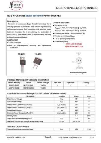
NCEP018N60,NCEP018N60D NCE N-Channel Super Trench II Power MOSFET Description General Features The series of devices uses Super Trench II technology that is V =60V,I =210A DS D uniquely optimized to provide the most efficient high frequency R =1.7m , typical (TO-220) @ V =10V DS(ON) GS switching performance. Both conduction and switching power R =1.5m , typical (TO-263) @ V =
nceap018n60agu.pdf
NCEAP018N60AGU http //www.ncepower.com NCE Automotive N-Channel Super Trench II Power MOSFET General Features Description V =60V,I =270A (Silicon Limited) DS D The NCEAP018N60AGU uses Super Trench II technology that is R =1.4 m (typical) @ V =10V DS(ON) GS uniquely optimized to provide the most efficient high frequency R =1.8 m (typical) @ V =4.5V DS(ON) GS switching perfor
ncep018n60gu.pdf
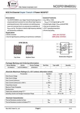
NCEP018N60GU http //www.ncepower.com NCE N-Channel Super Trench II Power MOSFET Description General Features The NCEP018N60GU uses Super Trench II technology that is V =60V,I =195A DS D uniquely optimized to provide the most efficient high frequency R =1.5 m (typical) @ V =10V DS(ON) GS switching performance. Both conduction and switching power Excellent gate charge x R produc
ncep018n60 ncep018n60d.pdf
NCEP018N60,NCEP018N60D NCE N-Channel Super Trench II Power MOSFET Description General Features The series of devices uses Super Trench II technology that is V =60V,I =210A DS D uniquely optimized to provide the most efficient high frequency R =1.7m , typical (TO-220) @ V =10V DS(ON) GS switching performance. Both conduction and switching power R =1.5m , typical (TO-263) @ V =
ncep028n60agu.pdf
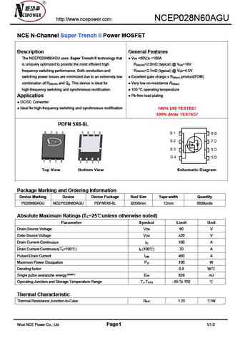
http //www.ncepower.com NCEP028N60AGU NCE N-Channel Super Trench II Power MOSFET Description General Features The NCEP028N60AGU uses Super Trench II technology that V =60V,I =100A DS D is uniquely optimized to provide the most efficient high R =2.0m (typical) @ V =10V DS(ON) GS frequency switching performance. Both conduction and R =2.7m (typical) @ V =4.5V DS(ON) GS switching
ncep018n60.pdf
NCEP018N60,NCEP018N60D NCE N-Channel Super Trench II Power MOSFET Description General Features The series of devices uses Super Trench II technology that is V =60V,I =210A DS D uniquely optimized to provide the most efficient high frequency R =1.7m , typical (TO-220) @ V =10V DS(ON) GS switching performance. Both conduction and switching power R =1.5m , typical (TO-263) @ V =
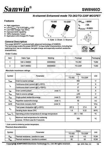
swu8n60d swf8n60d.pdf
SW8N60D N-channel Enhanced mode TO-262/TO-220F MOSFET Features TO-262 BVDSS 600V TO-220F ID 8A High ruggedness Low RDS(ON) (Typ 0.92 )@VGS=10V RDS(ON) 0.92 Low Gate Charge (Typ 29nC) Improved dv/dt Capability 2 100% Avalanche Tested 1 1 2 Application LED,Charger,PC Power 2 3 3 1. Gate 2. Drain 3. Source 1 General Descr
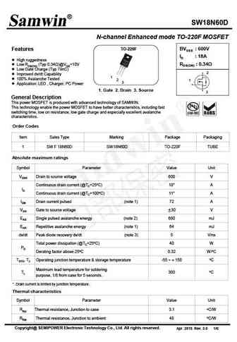
swf18n60d.pdf
SW18N60D N-channel Enhanced mode TO-220F MOSFET TO-220F BVDSS 600V Features ID 18A High ruggedness RDS(ON) 0.34 Low RDS(ON) (Typ 0.34 )@VGS=10V Low Gate Charge (Typ 79nC) 2 Improved dv/dt Capability 1 100% Avalanche Tested 2 1 3 Application LED , Charger, PC Power 1. Gate 2. Drain 3. Source 3 General Description This
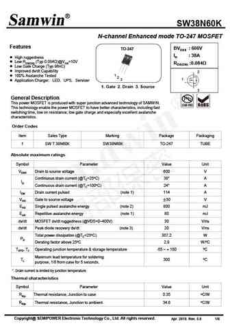
swt38n60k.pdf
SW38N60K N-channel Enhanced mode TO-247 MOSFET Features BVDSS 600V TO-247 ID 38A High ruggedness Low RDS(ON) (Typ 0.084 )@VGS=10V RDS(ON) 0.084 Low Gate Charge (Typ 96nC) Improved dv/dt Capability 2 1 100% Avalanche Tested 2 1 3 Application Charger LED UPS Servicer 1. Gate 2. Drain 3. Source 3 General Description
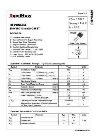
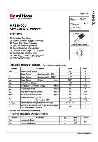
hfp8n60u.pdf
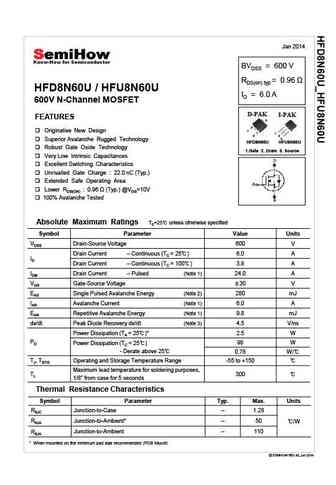
August 2012 BVDSS = 600 V RDS(on) typ HFP8N60U ID = 7.5 A 600V N-Channel MOSFET TO-220 FEATURES Originative New Design Superior Avalanche Rugged Technology 1 2 3 Robust Gate Oxide Technology 1.Gate 2. Drain 3. Source Very Low Intrinsic Capacitances Excellent Switching Characteristics Unrivalled Gate Charge 22.0 nC (Typ.) Extended Safe Operating Area
hfd8n60u.pdf
Jan 2014 BVDSS = 600 V RDS(on) typ HFD8N60U / HFU8N60U ID = 6.0 A 600V N-Channel MOSFET D-PAK I-PAK FEATURES 2 1 Originative New Design 1 3 2 3 Superior Avalanche Rugged Technology HFD8N60U HFU8N60U Robust Gate Oxide Technology 1.Gate 2. Drain 3. Source Very Low Intrinsic Capacitances Excellent Switching Characteristics Unrivalled Gate Charge 22.0 n
hfs8n60s.pdf
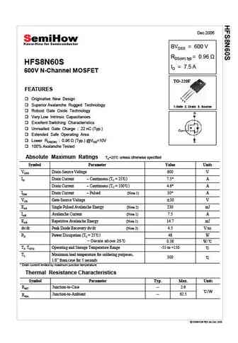
Dec 2006 BVDSS = 600 V RDS(on) typ HFS8N60S ID = 7.5 A 600V N-Channel MOSFET TO-220F FEATURES 1 Originative New Design 2 3 Superior Avalanche Rugged Technology 1.Gate 2. Drain 3. Source Robust Gate Oxide Technology Very Low Intrinsic Capacitances Excellent Switching Characteristics Unrivalled Gate Charge 22 nC (Typ.) Extended Safe Operating Area Lower RDS
hfp8n60s.pdf
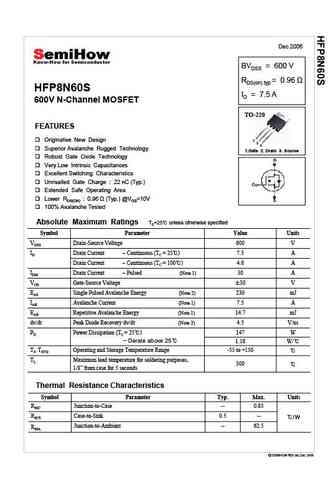
Dec 2006 BVDSS = 600 V RDS(on) typ HFP8N60S ID = 7.5 A 600V N-Channel MOSFET TO-220 FEATURES Originative New Design 1 2 3 Superior Avalanche Rugged Technology 1.Gate 2. Drain 3. Source Robust Gate Oxide Technology Very Low Intrinsic Capacitances Excellent Switching Characteristics Unrivalled Gate Charge 22 nC (Typ.) Extended Safe Operating Area Lower RDS(O
hfs8n60ua.pdf
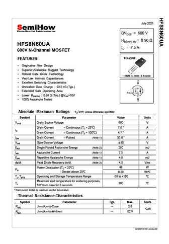
July 2021 BVDSS = 600 V RDS(on) typ = 0.96 HFS8N60UA ID = 7.5 A 600V N-Channel MOSFET TO-220F FEATURES Originative New Design Superior Avalanche Rugged Technology 1 2 3 Robust Gate Oxide Technology 1.Gate 2. Drain 3. Source Very Low Intrinsic Capacitances Excellent Switching Characteristics Unrivalled Gate Charge 22.0 nC (Typ.) Extended Safe
hfs8n60u.pdf
August 2012 BVDSS = 600 V RDS(on) typ HFS8N60U ID = 7.5 A 600V N-Channel MOSFET TO-220F FEATURES Originative New Design Superior Avalanche Rugged Technology 1 2 3 Robust Gate Oxide Technology 1.Gate 2. Drain 3. Source Very Low Intrinsic Capacitances Excellent Switching Characteristics Unrivalled Gate Charge 22.0 nC (Typ.) Extended Safe Operating Are
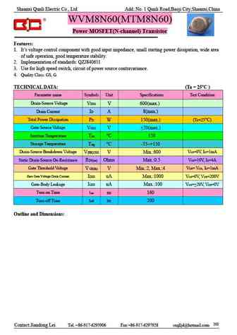
wvm8n60.pdf
Shaanxi Qunli Electric Co., Ltd Add. No. 1 Qunli Road,Baoji City,Shaanxi,China WVM8N60(MTM8N60) Power MOSFET(N-channel) Transistor Features 1. It s voltage control component with good input impedance, small starting power dissipation, wide area of safe operation, good temperature stability. 2. Implementation of standards QZJ840611 3. Use for high speed switch, circuit of power
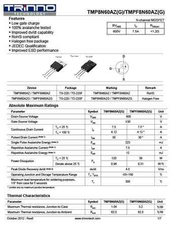
tmp8n60az tmpf8n60az.pdf
TMP8N60AZ(G)/TMPF8N60AZ(G) Features N-channel MOSFET Low gate charge BVDSS ID RDS(on) 100% avalanche tested 600V 7.5A
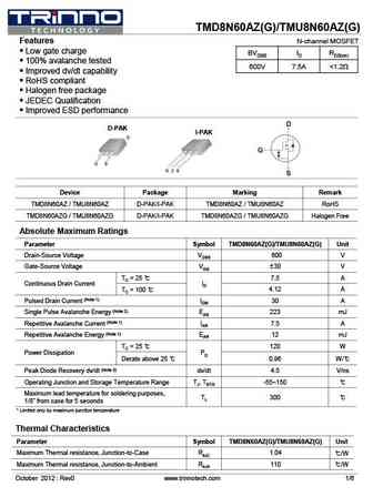
tmd8n60az tmu8n60az.pdf
TMD8N60AZ(G)/TMU8N60AZ(G) Features N-channel MOSFET Low gate charge BVDSS ID RDS(on) 100% avalanche tested 600V 7.5A
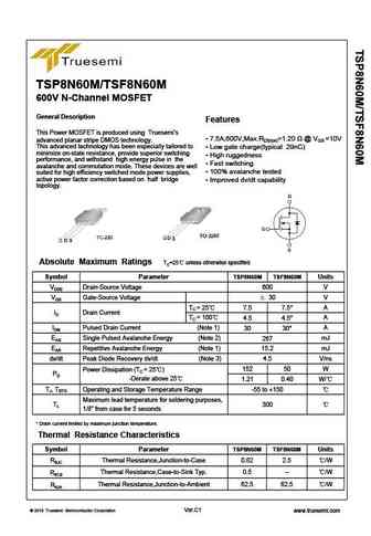
tsp8n60m tsf8n60m.pdf
TSP8N60M/TSF8N60M 600V N-Channel MOSFET General Description Features This Power MOSFET is produced using Truesemi s 7.5A,600V,Max.RDS(on)=1.20 @ VGS =10V advanced planar stripe DMOS technology. This advanced technology has been especially tailored to Low gate charge(typical 29nC) minimize on-state resistance, provide superior switching High ruggedness performance, an
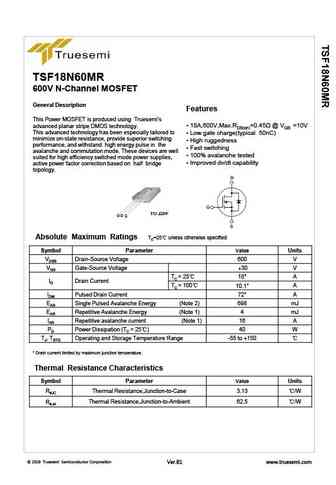
tsf18n60mr.pdf
TSF18N60MR 600V N-Channel MOSFET General Description Features This Power MOSFET is produced using Truesemi s 18A,600V,Max.RDS(on)=0.45 @ VGS =10V advanced planar stripe DMOS technology. This advanced technology has been especially tailored to Low gate charge(typical 50nC) minimize on-state resistance, provide superior switching High ruggedness performance, and
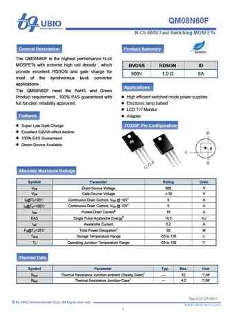
qm08n60f.pdf
QM08N60F 1 2011-11-15 - 1 - N-Ch 600V Fast Switching MOSFETs General Description Product Summery The QM08N60F is the highest performance N-ch MOSFETs with extreme high cell density , which BVDSS RDSON ID provide excellent RDSON and gate charge for 600V 1.0 8A most of the synchronous buck converter applications . Applications The QM08N60F meet the RoHS and
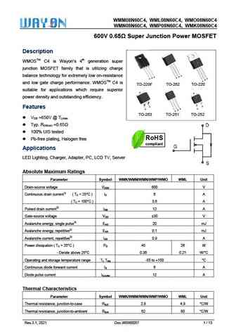
wmm08n60c4 wml08n60c4 wmo08n60c4 wmn08n60c4 wmp08n60c4 wmk08n60c4.pdf
WMM0 60C4, MO08N60C 08N60C4, WML08N6 WM C4 WMN0 60C4, MK08N60C 08N60C4, WMP08N6 WM C4 600V 0.65 S T V Super Junction Power MOSFET Descrip ption WMOSTM C4 is Wa 4th generation super ayon s n junction MOSFET fa that is utilizing charge M amily S balance te or extremely esistance echnology fo y low on-re D S D G G G S D G and low ga charge performanc WM
wml28n60c4 wmk28n60c4 wmn28n60c4 wmm28n60c4 wmj28n60c4.pdf
WML28N6 WM C4 60C4, MK28N60C WMN2 MJ28N60C 28N60C4, WMM28N60C4, WM C4 600V 0.13 S T V Super Junction Power MOSFET Descrip ption WMOSTM C4 is Wa 4th generation super ayon s n junction MOSFET fa that is utilizing charge M amily S balance te or extremely esistance echnology fo y low on-re S D D G G G S D G and low ga charge performanc WMOSTM C4 is ate c
wml28n60f2 wmk28n60f2 wmn28n60f2 wmm28n60f2 wmj28n60f2.pdf
WML28N60F2, WM F2 MK28N60F WMN2 N60F2, WM F2 28N60F2, WMM28N MJ28N60F 600V 0.15 S T V Super Junction Power MOSFET Descrip ption WMOSTM F2 is Wa 2nd generation super ayon s junction MOSFET fam with fa body di F2 M mily ast iode. S series pro all benefits of a fast switching ovide b f s S D D G G G S D G SJ-MOSFE while of an extremely fa body ET fferin
cs8n60fa9h.pdf
Silicon N-Channel Power MOSFET R CS8N60F A9H General Description VDSS 600 V CS8N60F A9H, the silicon N-channel Enhanced ID 8 A PD(TC=25 ) 45 W VDMOSFETs, is obtained by the self-aligned planar Technology RDS(ON)Typ 0.8 which reduce the conduction loss, improve switching performance and enhance the avalanche energy. The transistor can be used in various powe
cs8n60a8h.pdf
Huajing Discrete Devices R Silicon N-Channel Power MOSFET CS8N60 A8H General Description VDSS 600 V CS8N60 A8H, the silicon N-channel Enhanced ID 8 A PD(TC=25 ) 110 W VDMOSFETs, is obtained by the self-aligned planar Technology RDS(ON)Typ 0.8 which reduce the conduction loss, improve switching performance and enhance the avalanche energy. The transistor c
cs8n60f cs8n60p cs8n60u cs8n60d cs8n65f-b.pdf
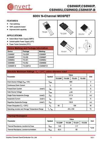
CS8N60F,CS8N60P, nvert Suzhou Convert Semiconductor Co ., Ltd. CS8N60U,CS8N60D,CS8N65F-B 600V N-Channel MOSFET FEATURES Fast switching 100% avalanche tested Improved dv/dt capability APPLICATIONS Switch Mode Power Supply (SMPS) Uninterruptible Power Supply (UPS) Power Factor Correction (PFC) Device Marking and Package Information Device Package Marking CS
cs8n60f cs8n60p cs8n60u cs8n60d.pdf
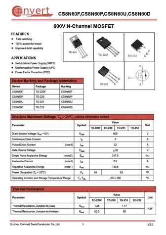
nvert CS8N60F,CS8N60P,CS8N60U,CS8N60D Suzhou Convert Semiconductor Co ., Ltd. 600V N-Channel MOSFET FEATURES Fast switching 100% avalanche tested Improved dv/dt capability APPLICATIONS Switch Mode Power Supply (SMPS) Uninterruptible Power Supply (UPS) Power Factor Correction (PFC) Device Marking and Package Information Device Package Marking CS8N60F TO-220F
fir8n60fg.pdf
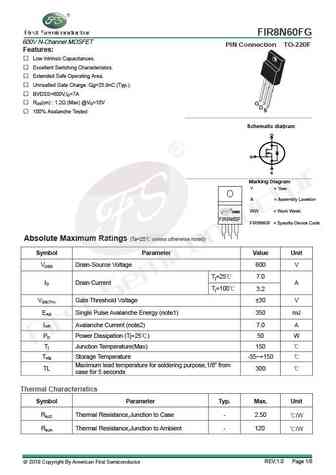
FIR8N60FG 600V N-Channel MOSFET PIN Connection TO-220F Features Low Intrinsic Capacitances. Excellent Switching Characteristics. Extended Safe Operating Area. Unrivalled Gate Charge Qg=25.9nC (Typ.). BVDSS=600V,ID=7A RDS(on) 1.2 (Max) @VG=10V G D S 100% Avalanche Tested g Schematic dia ram D G S Marking Diagram Y = Year A = Assembly
smt8n60.pdf
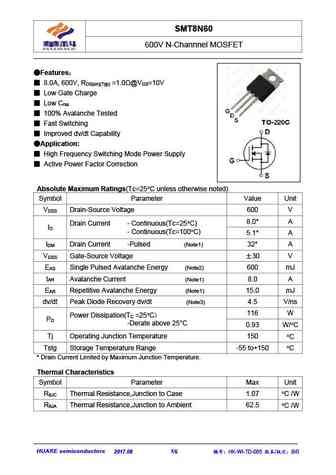
SMT8N60 600V N-Channnel MOSFET Features 8.0A, 600V, R =1.0 @V =10V DS(on)(Typ) GS Low Gate Charge Low C rss 100% Avalanche Tested Fast Switching Improved dv/dt Capability Application High Frequency Switching Mode Power Supply Active Power Factor Correction Absolute Maximum Ratings(Tc=25 C unless otherwise noted) Symbol Parameter Value
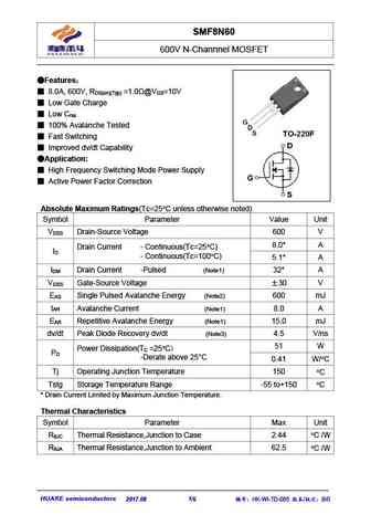
smf8n60.pdf
SMF8N60 600V N-Channnel MOSFET Features 8.0A, 600V, R =1.0 @V =10V DS(on)(Typ) GS Low Gate Charge Low C rss 100% Avalanche Tested Fast Switching Improved dv/dt Capability Application High Frequency Switching Mode Power Supply Active Power Factor Correction Absolute Maximum Ratings(Tc=25 C unless otherwise noted) Symbol Parameter Value
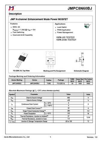
jmpc8n60bj.pdf
JMPC8N60BJ Description JMP N-channel Enhancement Mode Power MOSFET Features Applications 600V, 8A Load Switch RDS(ON)
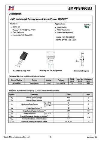
jmpf8n60bj.pdf
JMPF8N60BJ Description JMP N-channel Enhancement Mode Power MOSFET Features Applications 600V, 8A Load Switch RDS(ON)
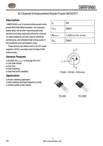
smirf8n60.pdf
SMIRF8N60 30V /36A Single N Power MOSFET N-Channel Enhancement Mode Power MOSFET Description ID 8A SMIRF8N60 is an N-channel enhancement mode power MOS field effect transistor. The improved VDSS 600V planar stripe cell and the improved guard ring terminal have been especially tailored to minimize Rdson(max) 1.2 (VGS=10V, ID=4A) on-state resistance, provide superior switchi
vbzm8n60.pdf
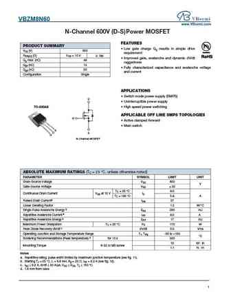
VBZM8N60 www.VBsemi.com N hannel 600 D S P ower MOSFET FEATURES PRODUCT SUMMARY Low gate charge Qg results in simple drive VDS (V) 600 Available requirement RDS(on) ( )VGS = 10 V 0.780 Improved gate, avalanche and dynamic dV/dt Qg max. (nC) 49 ruggedness Qgs (nC) 13 Fully characterized capacitance and avalanche voltage Qgd (nC) 20 and current Configuration Si
vbzmb8n60.pdf
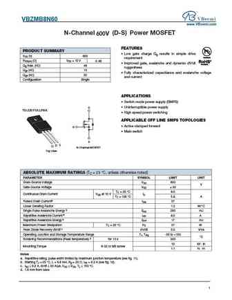
VBZMB8N60 www.VBsemi.com N-Channel (D-S) Power MOSFET 600V FEATURES PRODUCT SUMMARY Low gate charge Qg results in simple drive VDS (V) 600 Available requirement RDS(on) ( )VGS = 10 V 0.88 Improved gate, avalanche and dynamic dV/dt Available Qg max. (nC) 49 ruggedness Qgs (nC) 13 Fully characterized capacitance and avalanche voltage Qgd (nC) 20 and current Conf
tma8n60h tmd8n60h tmu8n60h.pdf
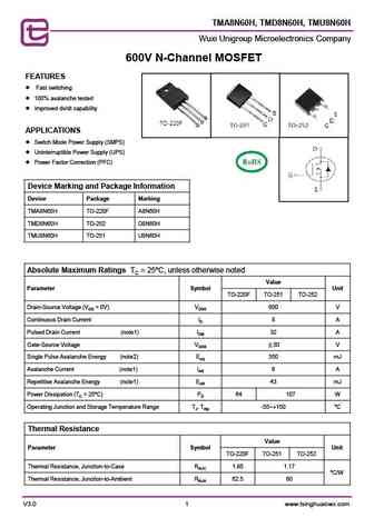
TMA8N60H, TMD8N60H, TMU8N60H Wuxi Unigroup Microelectronics Company 600V N-Channel MOSFET FEATURES Fast switching 100% avalanche tested Improved dv/dt capability APPLICATIONS Switch Mode Power Supply (SMPS) Uninterruptible Power Supply (UPS) Power Factor Correction (PFC) Device Marking and Package Information Device Package Marking TMA8N60H TO-
hms8n60k hms8n60i.pdf
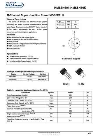
HMS8N60I, HMS8N60K N-Channel Super Junction Power MOSFET General Description The series of devices use advanced super junction VDS@Tjmax 650 V technology and design to provide excellent RDS(ON) with low RDS(ON) MAX 540 m gate charge. This super junction MOSFET fits the industry s ID 8 A AC-DC SMPS requirements for PFC, AC/DC power conversion, and industrial power applicati
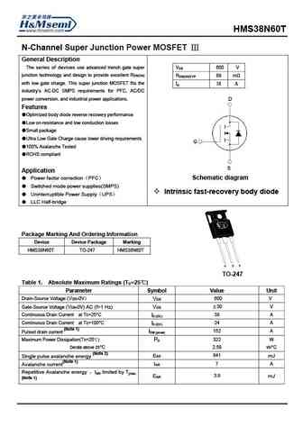
hms38n60t.pdf
HMS38N60T N-Channel Super Junction Power MOSFET General Description The series of devices use advanced trench gate super V 600 V DS junction technology and design to provide excellent RDS(ON) R 89 m DS(ON)TYP with low gate charge. This super junction MOSFET fits the ID 38 A industry s AC-DC SMPS requirements for PFC, AC/DC power conversion, and industrial power applic
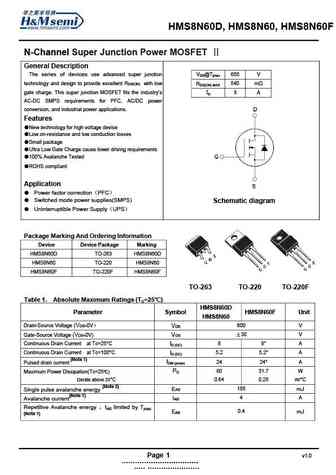
hms8n60 hms8n60f hms8n60d.pdf
HMS8N60D, HMS8N60, HMS8N60F N-Channel Super Junction Power MOSFET General Description The series of devices use advanced super junction VDS@Tjmax 650 V technology and design to provide excellent RDS(ON) with low RDS(ON) MAX 540 m gate charge. This super junction MOSFET fits the industry s ID 8 A AC-DC SMPS requirements for PFC, AC/DC power conversion, and industrial power
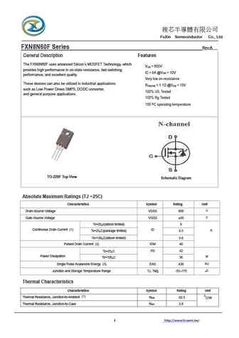
fxn8n60f.pdf
FuXin Semiconductor Co., Ltd. FXN8N60F Series Rev.A General Description Features The FXN8N60F uses advanced Silicon s MOSFET Technology, which V = 600V DS provides high performance in on-state resistance, fast switching ID = 8A @V = 10V GS performance, and excellent quality. Very low on-resistance These devices can also be utilized in industrial appl
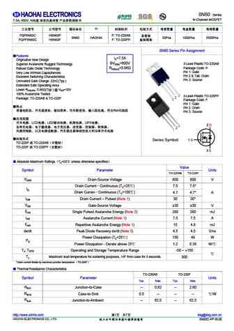
h8n60p h8n60f.pdf
8N60 Series N-Channel MOSFET 7.5A, 600V, N H FQP8N60C H8N60P P TO-220AB 8N60 HAOHAI 50Pcs 1000Pcs 5000Pcs FQPF8N60C H8N60F F TO-220FP 8N60 Series Pin Assignment Features ID=7.5A Originative New Design
18n60.pdf
INCHANGE Semiconductor isc N-Channel MOSFET Transistor 18N60 FEATURES With TO-247 packaging High speed switching Standard level gate drive Easy to use 100% avalanche tested Minimum Lot-to-Lot variations for robust device performance and reliable operation APPLICATIONS Power supply Switching applications ABSOLUTE MAXIMUM RATINGS(T =25 ) a SYMBOL PARAMETER V
mdp8n60th.pdf
isc N-Channel MOSFET Transistor MDP8N60TH FEATURES Drain Current I = 8A@ T =25 D C Drain Source Voltage V = 600V(Min) DSS Static Drain-Source On-Resistance R = 1.0 (Max) @V = 10V DS(on) GS 100% avalanche tested Minimum Lot-to-Lot variations for robust device performance and reliable operation DESCRIPTION motor drive, DC-DC converter, power switch and solenoi
aotf8n60.pdf
isc N-Channel MOSFET Transistor AOTF8N60 FEATURES Drain Current I = 8A@ T =25 D C Drain Source Voltage- V = 600V(Min) DSS Static Drain-Source On-Resistance R = 0.9 (Max) DS(on) 100% avalanche tested Minimum Lot-to-Lot variations for robust device performance and reliable operation DESCRIPTION Designed for use in switch mode power supplies and general purpos
aot8n60.pdf
isc N-Channel MOSFET Transistor AOT8N60 FEATURES Drain Current I = 8A@ T =25 D C Drain Source Voltage- V = 600V(Min) DSS Static Drain-Source On-Resistance R = 0.9 (Max) DS(on) 100% avalanche tested Minimum Lot-to-Lot variations for robust device performance and reliable operation DESCRIPTION Designed for use in switch mode power supplies and general purpose
stf18n60m2.pdf
isc N-Channel MOSFET Transistor STF18N60M2 FEATURES With TO-220F packaging High speed switching Low gate input resistance Standard level gate drive Easy to use 100% avalanche tested Minimum Lot-to-Lot variations for robust device performance and reliable operation APPLICATIONS Power supply Switching applications ABSOLUTE MAXIMUM RATINGS(T =25 ) a SYMBOL
apt38n60bc6.pdf
isc N-Channel MOSFET Transistor APT38N60BC6 FEATURES Drain Current I =38A@ T =25 D C Drain Source Voltage- V =600V(Min) DSS Static Drain-Source On-Resistance R =0.099 (Max) DS(on) 100% avalanche tested Minimum Lot-to-Lot variations for robust device performance and reliable operation DESCRIPTION Designed for use in switch mode power supplies and general pur
Другие IGBT... 6N65, 5N60, 6N60, 6N60Z, 7N60A, 7N60, 7N60Z, 7N60K, AO4407, 10N60, 10N60K, 12N60, 15N60, 18N60, 20N60, 22N60, UF601
Параметры MOSFET. Взаимосвязь и компромиссы
🌐 : EN ES РУ
Список транзисторов
Обновления
MOSFET: BC3134KT | BC3134K | BC2302W | BC2302T-2.8A | BC2302-2.8A | BC2301W | BC2301T-2.8A | CB3139KTB | CB2301DW | BC8205 | BC3415 | BC3407 | BC3401 | BC3400 | BC2301 | BC1012W
Popular searches
2sc2240 transistor | c3198 | 2sc793 | 2sd313 replacement | 2n4249 | a1013 transistor | 2sc2705 | bc239
