18N60 datasheet, аналоги, основные параметры
Наименование производителя: 18N60 📄📄
Тип транзистора: MOSFET
Полярность: N
Предельные значения
Pd ⓘ - Максимальная рассеиваемая мощность: 360 W
|Vds|ⓘ - Максимально допустимое напряжение сток-исток: 600 V
|Vgs|ⓘ - Максимально допустимое напряжение затвор-исток: 30 V
|Id| ⓘ - Максимально допустимый постоянный ток стока: 18 A
Tj ⓘ - Максимальная температура канала: 150 °C
Электрические характеристики
tr ⓘ - Время нарастания: 22 ns
Cossⓘ - Выходная емкость: 280 pf
RDSonⓘ - Сопротивление сток-исток открытого транзистора: 0.36 Ohm
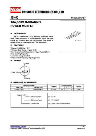
Тип корпуса: TO-247
TO-3P
📄📄 Копировать
Аналог (замена) для 18N60
- подборⓘ MOSFET транзистора по параметрам
18N60 даташит
..2. Size:212K inchange semiconductor
18n60.pdf 
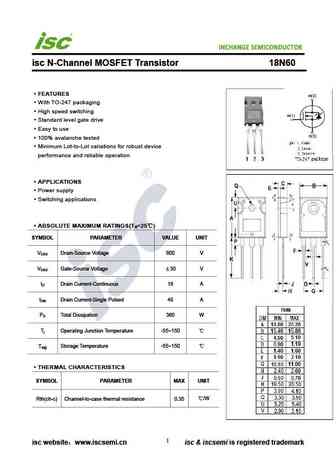
INCHANGE Semiconductor isc N-Channel MOSFET Transistor 18N60 FEATURES With TO-247 packaging High speed switching Standard level gate drive Easy to use 100% avalanche tested Minimum Lot-to-Lot variations for robust device performance and reliable operation APPLICATIONS Power supply Switching applications ABSOLUTE MAXIMUM RATINGS(T =25 ) a SYMBOL PARAMETER V
0.1. Size:287K st
stp18n60dm2.pdf 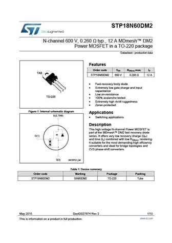
STP18N60DM2 N-channel 600 V, 0.260 typ., 12 A MDmesh DM2 Power MOSFET in a TO-220 package Datasheet - production data Features Order code V R max. I DS DS(on) D STP18N60DM2 600 V 0.295 12 A Fast-recovery body diode Extremely low gate charge and input capacitance Low on-resistance 100% avalanche tested Extremely high dv/dt ruggedness Ze
0.2. Size:627K st
stfh18n60m2.pdf 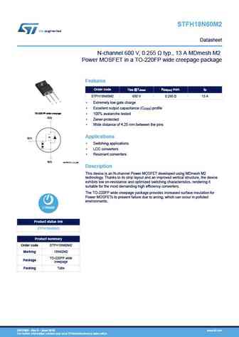
STFH18N60M2 Datasheet N-channel 600 V, 0.255 typ., 13 A MDmesh M2 Power MOSFET in a TO-220FP wide creepage package Features VDS @TJmax RDS(on) max. ID Order code STFH18N60M2 650 V 0.280 13 A Extremely low gate charge Excellent output capacitance (COSS) profile TO-220 FP wide creepage 100% avalanche tested D(2) Zener-protected Wide distance of 4.25 mm bet
0.3. Size:1200K st
stb18n60m2 stp18n60m2 stw18n60m2.pdf 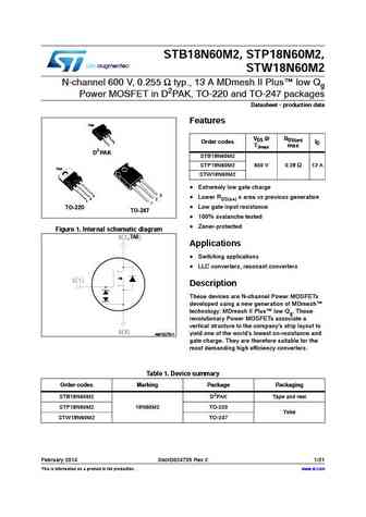
STB18N60M2, STP18N60M2, STW18N60M2 N-channel 600 V, 0.255 typ., 13 A MDmesh II Plus low Qg Power MOSFET in D2PAK, TO-220 and TO-247 packages Datasheet - production data Features TAB VDS @ RDS(on) 3 Order codes ID 1 TJmax max 2 D PAK STB18N60M2 STP18N60M2 650 V 0.28 13 A TAB STW18N60M2 Extremely low gate charge 3 3 Lower RDS(on) x area vs previous generation
0.4. Size:1066K st
stf18n60m2.pdf 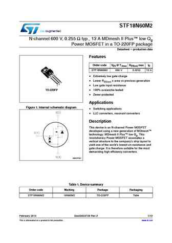
STF18N60M2 N-channel 600 V, 0.255 typ., 13 A MDmesh II Plus low Qg Power MOSFET in a TO-220FP package Datasheet - production data Features Order code VDS @ TJmax RDS(on) max ID STF18N60M2 650 V 0.28 13 A Extremely low gate charge Lower RDS(on) x area vs previous generation 3 2 1 Low gate input resistance TO-220FP 100% avalanche tested Zener-protected
0.5. Size:940K st
stl18n60m2.pdf 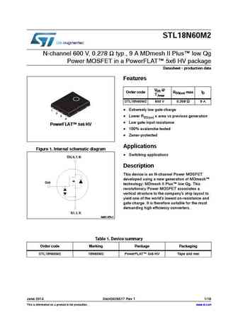
STL18N60M2 N-channel 600 V, 0.278 typ., 9 A MDmesh II Plus low Qg Power MOSFET in a PowerFLAT 5x6 HV package Datasheet - production data Features VDS @ Order code TJmax RDS(on) max ID STL18N60M2 650 V 0.308 9 A Extremely low gate charge 1 2 3 Lower RDS(on) x area vs previous generation 4 Low gate input resistance PowerFLAT 5x6 HV 100% avalanche
0.7. Size:183K ixys
ixfa18n60x ixfh18n60x ixfp18n60x.pdf 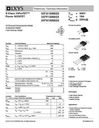
Preliminary Technical Information X-Class HiPerFETTM VDSS = 600V IXFA18N60X Power MOSFET ID25 = 18A IXFP18N60X RDS(on) 230m IXFH18N60X TO-263 AA (IXFA) N-Channel Enhancement Mode Avalanche Rated Fast Intrinsic Diode G S D (Tab) TO-220AB (IXFP) Symbol Test Conditions Maximum Ratings VDSS TJ = 25 C to 150 C 600 V VDGR TJ = 25 C to
0.8. Size:172K ixys
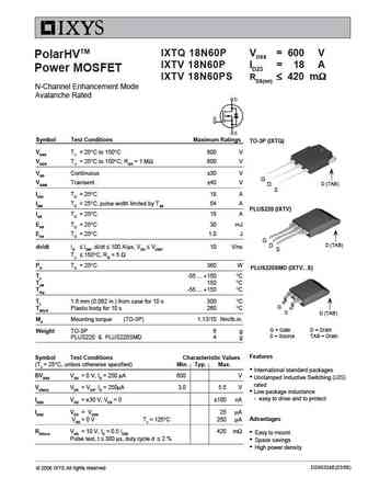
ixfh18n60p ixfv18n60p.pdf 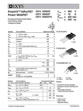
IXFH 18N60P VDSS = 600 V PolarHVTM HiPerFET IXFV 18N60P ID25 = 18 A Power MOSFET IXFV 18N60PS RDS(on) 400 m N-Channel Enhancement Mode trr 200 ns Fast Intrinsic Diode Avalanche Rated Symbol Test Conditions Maximum Ratings TO-247 AD (IXFH) VDSS TJ = 25 C to 150 C 600 V VDGR TJ = 25 C to 150 C; RGS = 1 M 600 V VGS Co
0.10. Size:503K jiaensemi
jfpc18n60ci.pdf 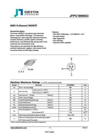
JFPC18N60CI 600V N-Channel MOSFET General Description Features This Power MOSFET is produced using advanced - 18A, 600V, RDS(on)typ. = 0.52 @VGS = 10 V planar stripe DMOS technology. This advanced - Low gate charge technology has been especially tailored to minimize - High ruggedness on-state resistance, provide superior switching - Fast switching performance, and withs
0.11. Size:862K jiaensemi
jfpc18n60c jffm18n60c.pdf 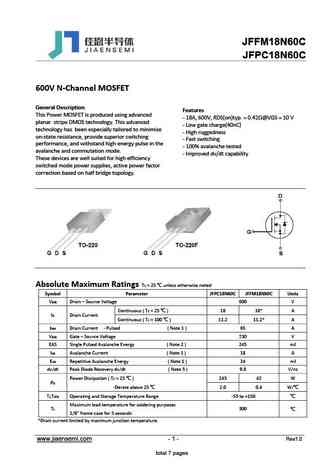
JFFM18N60C JFPC18N60C 600V N-Channel MOSFET General Description Features This Power MOSFET is produced using advanced - 18A, 600V, RDS(on)typ. = 0.42 @VGS = 10 V planar stripe DMOS technology. This advanced - Low gate charge(40nC) technology has been especially tailored to minimize - High ruggedness on-state resistance, provide superior switching - Fast switching perf
0.12. Size:1129K ncepower
ncep018n60agu.pdf 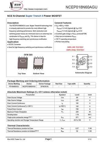
NCEP018N60AGU http //www.ncepower.com NCE N-Channel Super Trench II Power MOSFET Description General Features The NCEP018N60AGU uses Super Trench II technology that V =60V,I =195A DS D is uniquely optimized to provide the most efficient high R =1.4 m (typical) @ V =10V DS(ON) GS frequency switching performance. Both conduction and R =1.8 m (typical) @ V =4.5V DS(ON) GS switchi
0.13. Size:815K ncepower
nceap018n60gu.pdf 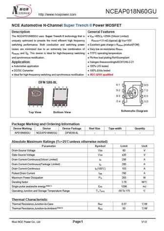
NCEAP018N60GU http //www.ncepower.com NCE Automotive N-Channel Super Trench II Power MOSFET Description General Features The NCEAP018N60GU uses Super Trench II technology that is V =60V,I =256A (Silicon Limited) DS D uniquely optimized to provide the most efficient high frequency R =1.6 m (typical) @ V =10V DS(ON) GS switching performance. Both conduction and switching power E
0.14. Size:686K ncepower
ncep018n60d.pdf 
NCEP018N60,NCEP018N60D NCE N-Channel Super Trench II Power MOSFET Description General Features The series of devices uses Super Trench II technology that is V =60V,I =210A DS D uniquely optimized to provide the most efficient high frequency R =1.7m , typical (TO-220) @ V =10V DS(ON) GS switching performance. Both conduction and switching power R =1.5m , typical (TO-263) @ V =
0.15. Size:822K ncepower
nceap018n60agu.pdf 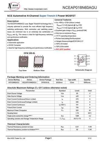
NCEAP018N60AGU http //www.ncepower.com NCE Automotive N-Channel Super Trench II Power MOSFET General Features Description V =60V,I =270A (Silicon Limited) DS D The NCEAP018N60AGU uses Super Trench II technology that is R =1.4 m (typical) @ V =10V DS(ON) GS uniquely optimized to provide the most efficient high frequency R =1.8 m (typical) @ V =4.5V DS(ON) GS switching perfor
0.16. Size:1124K ncepower
ncep018n60gu.pdf 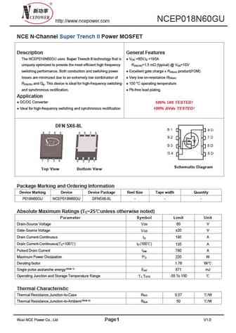
NCEP018N60GU http //www.ncepower.com NCE N-Channel Super Trench II Power MOSFET Description General Features The NCEP018N60GU uses Super Trench II technology that is V =60V,I =195A DS D uniquely optimized to provide the most efficient high frequency R =1.5 m (typical) @ V =10V DS(ON) GS switching performance. Both conduction and switching power Excellent gate charge x R produc
0.17. Size:686K ncepower
ncep018n60 ncep018n60d.pdf 
NCEP018N60,NCEP018N60D NCE N-Channel Super Trench II Power MOSFET Description General Features The series of devices uses Super Trench II technology that is V =60V,I =210A DS D uniquely optimized to provide the most efficient high frequency R =1.7m , typical (TO-220) @ V =10V DS(ON) GS switching performance. Both conduction and switching power R =1.5m , typical (TO-263) @ V =
0.18. Size:686K ncepower
ncep018n60.pdf 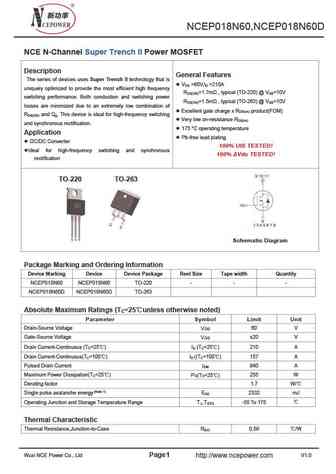
NCEP018N60,NCEP018N60D NCE N-Channel Super Trench II Power MOSFET Description General Features The series of devices uses Super Trench II technology that is V =60V,I =210A DS D uniquely optimized to provide the most efficient high frequency R =1.7m , typical (TO-220) @ V =10V DS(ON) GS switching performance. Both conduction and switching power R =1.5m , typical (TO-263) @ V =
0.19. Size:814K samwin
swf18n60d.pdf 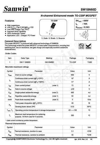
SW18N60D N-channel Enhanced mode TO-220F MOSFET TO-220F BVDSS 600V Features ID 18A High ruggedness RDS(ON) 0.34 Low RDS(ON) (Typ 0.34 )@VGS=10V Low Gate Charge (Typ 79nC) 2 Improved dv/dt Capability 1 100% Avalanche Tested 2 1 3 Application LED , Charger, PC Power 1. Gate 2. Drain 3. Source 3 General Description This
0.20. Size:896K truesemi
tsf18n60mr.pdf 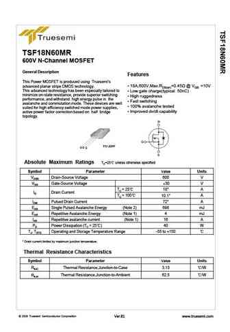
TSF18N60MR 600V N-Channel MOSFET General Description Features This Power MOSFET is produced using Truesemi s 18A,600V,Max.RDS(on)=0.45 @ VGS =10V advanced planar stripe DMOS technology. This advanced technology has been especially tailored to Low gate charge(typical 50nC) minimize on-state resistance, provide superior switching High ruggedness performance, and
0.21. Size:255K inchange semiconductor
stf18n60m2.pdf 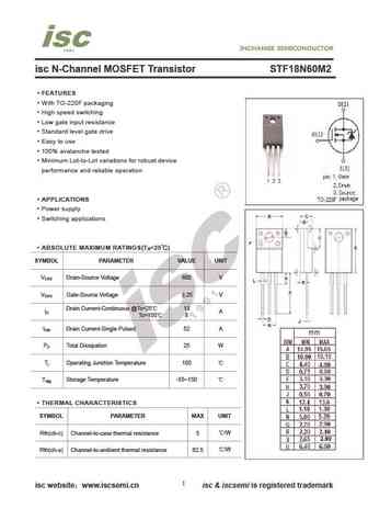
isc N-Channel MOSFET Transistor STF18N60M2 FEATURES With TO-220F packaging High speed switching Low gate input resistance Standard level gate drive Easy to use 100% avalanche tested Minimum Lot-to-Lot variations for robust device performance and reliable operation APPLICATIONS Power supply Switching applications ABSOLUTE MAXIMUM RATINGS(T =25 ) a SYMBOL
Другие IGBT... 7N60, 7N60Z, 7N60K, 8N60, 10N60, 10N60K, 12N60, 15N60, 60N06, 20N60, 22N60, UF601, UK2996, 1N60A, 1N60, 1N60P, 1N60Z