2N60 datasheet, аналоги, основные параметры
Наименование производителя: 2N60 📄📄
Тип транзистора: MOSFET
Полярность: N
Предельные значения
Pd ⓘ - Максимальная рассеиваемая мощность: 54 W
|Vds|ⓘ - Максимально допустимое напряжение сток-исток: 600 V
|Vgs|ⓘ - Максимально допустимое напряжение затвор-исток: 30 V
|Id| ⓘ - Максимально допустимый постоянный ток стока: 2 A
Tj ⓘ - Максимальная температура канала: 150 °C
Электрические характеристики
tr ⓘ - Время нарастания: 35 ns
Cossⓘ - Выходная емкость: 45 pf
RDSonⓘ - Сопротивление сток-исток открытого транзистора: 3.6 Ohm
Тип корпуса: TO-262 TO-251 TO-252 TO-220 TO-220F TO-126 DFN-8
📄📄 Копировать
Аналог (замена) для 2N60
- подборⓘ MOSFET транзистора по параметрам
2N60 даташит
2n60.pdf
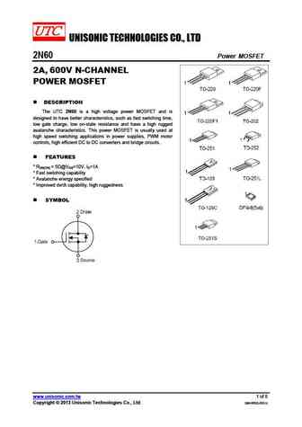
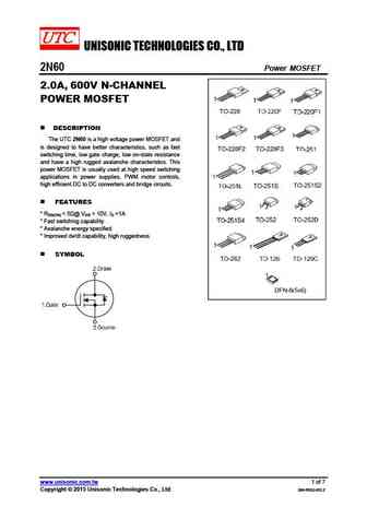
UNISONIC TECHNOLOGIES CO., LTD 2N60 Power MOSFET 2A, 600V N-CHANNEL POWER MOSFET DESCRIPTION The UTC 2N60 is a high voltage power MOSFET and is designed to have better characteristics, such as fast switching time, low gate charge, low on-state resistance and have a high rugged avalanche characteristics. This power MOSFET is usually used at high speed switching applications
2n60.pdf
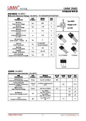
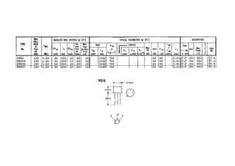
R UMW UMW 2N60 UMW 2N60 N- MOS N- MOS N- MOS N- MOS Tc=25 C Tc=25 C Tc=25 C Tc=25 C Absolute Maximum Ratings Tc=25 C Absolute Maximum Ratings Tc=25 C Absolute Maximum Ratings Tc=25 C TO-220/220F/251T/252/223 Absolute Maximum Ratings Tc=25 C PARAMETER SYMBOL VALUE UNIT PARAMETER SYMBOL VALUE
2n60 .pdf
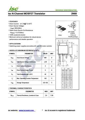
isc N-Channel MOSFET Transistor 2N60 FEATURES Drain Current I = 2A@ T =25 D C Drain Source Voltage- V = 600V(Min) DSS Static Drain-Source On-Resistance R = 5.0 (Max) DS(on) 100% avalanche tested Minimum Lot-to-Lot variations for robust device performance and reliable operation APPLICATIONS Switching power supplies,converters,AC and DC motor controls ABSO
2n60.pdf
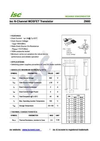
isc N-Channel MOSFET Transistor 2N60 FEATURES Drain Current I = 2A@ T =25 D C Drain Source Voltage- V = 600V(Min) DSS Static Drain-Source On-Resistance R = 5.0 (Max) DS(on) 100% avalanche tested Minimum Lot-to-Lot variations for robust device performance and reliable operation APPLICATIONS Switching power supplies,converters,AC and DC motor controls ABSO
hgtp12n60d1.pdf
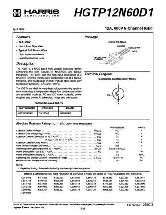
S E M I C O N D U C T O R HGTP12N60D1 12A, 600V N-Channel IGBT April 1995 Features Package JEDEC TO-220AB 12A, 600V EMITTER Latch Free Operation COLLECTOR Typical Fall Time
fhp12n60.pdf
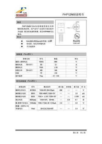
FHP12N60 FHP12N60 N MOS AC-DC DC-DC H PMW 12A,600V,RDS(on)( 0.6 TC=25 VDS
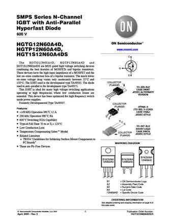
hgtp12n60a4 hgtg12n60a4 hgt1s12n60a4s.pdf
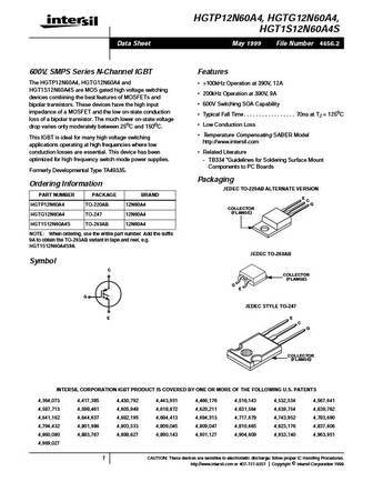
HGTP12N60A4, HGTG12N60A4, HGT1S12N60A4S Data Sheet May 1999 File Number 4656.2 600V, SMPS Series N-Channel IGBT Features The HGTP12N60A4, HGTG12N60A4 and >100kHz Operation at 390V, 12A HGT1S12N60A4S are MOS gated high voltage switching 200kHz Operation at 390V, 9A devices combining the best features of MOSFETs and 600V Switching SOA Capability bipolar transistors. These de
pfb2n60 pff2n60.pdf
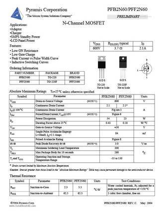
Pyramis Corporation PFB2N60/PFF2N60 The Silicon System Solutions Company www.DataSheet4U.com PRELIMINARY N-Channel MOSFET Applications Adaptor Charger SMPS Standby Power LCD Panel Power VDSS RDS(ON) typical ID Features 600V 3.7 2.1A Low ON Resistance Low Gate Charge Peak Current vs Pulse Width Curve Inductive Switching Curves Ordering In
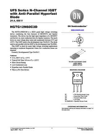
hgt1s12n60c3s9a.pdf
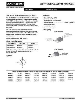
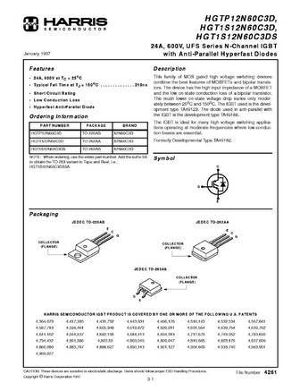
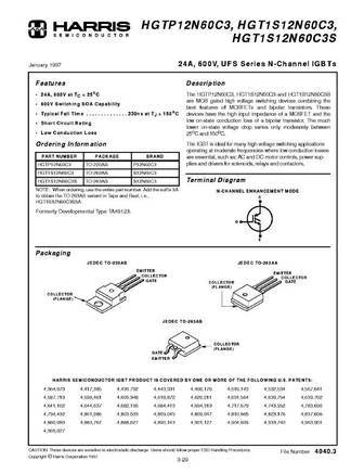
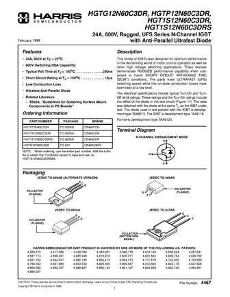
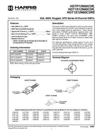
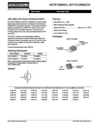
HGTP12N60C3, HGT1S12N60C3S Data Sheet December 2001 24A, 600V, UFS Series N-Channel IGBTs Features The HGTP12N60C3 and HGT1S12N60C3S are MOS gated 24A, 600V at TC = 25oC high voltage switching devices combining the best features 600V Switching SOA Capability of MOSFETs and bipolar transistors. These devices have the Typical Fall Time. . . . . . . . . . . . . . . . 230ns a
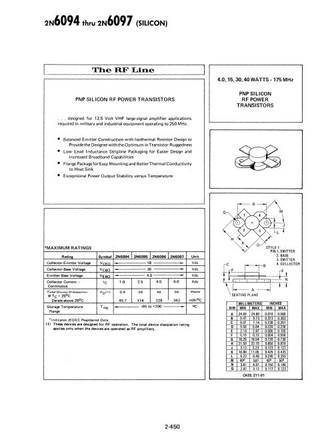
2n6027 2n6028.pdf
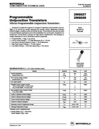
MOTOROLA Order this document SEMICONDUCTOR TECHNICAL DATA by 2N6027/D 2N6027 Programmable 2N6028 Unijunction Transistors Silicon Programmable Unijunction Transistors . . . designed to enable the engineer to program unijunction characteristics such as PUTs RBB, , IV, and IP by merely selecting two resistor values. Application includes 40 VOLTS thyristor-trigger, oscillator,
2n6071 2n6073 2n6075.pdf
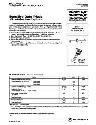
MOTOROLA Order this document SEMICONDUCTOR TECHNICAL DATA by 2N6071/D * 2N6071A,B * 2N6073A,B Sensitive Gate Triacs 2N6075A,B* Silicon Bidirectional Thyristors *Motorola preferred devices . . . designed primarily for full-wave ac control applications, such as light dimmers, motor controls, heating controls and power supplies; or wherever full-wave silicon gate controlled solid-sta
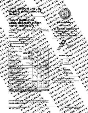
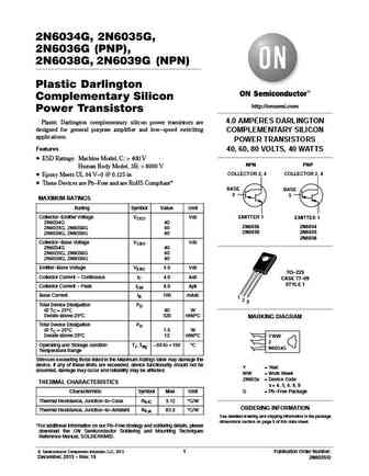
2n6035 2n6036 2n6038 2n6039.pdf

Order this document MOTOROLA by 2N6035/D SEMICONDUCTOR TECHNICAL DATA 2N6030 thru 2N6031 (See 2N5630) Plastic Darlington Complementary Silicon Power PNP Transistors 2N6035 . . . designed for general purpose amplifier and low speed switching applications. High DC Current Gain 2N6036* hFE = 2000 (Typ) @ IC = 2.0 Adc NPN Collector Emitter Sustaining Voltage @
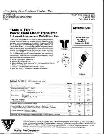
mtp2n60e.pdf

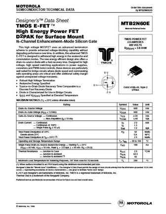
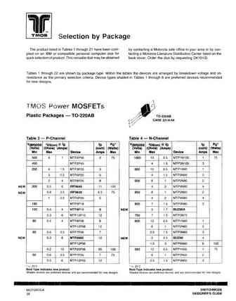
MOTOROLA Order this document SEMICONDUCTOR TECHNICAL DATA by MTP2N60E/D Designer's Data Sheet MTP2N60E TMOS E-FET. Motorola Preferred Device Power Field Effect Transistor N Channel Enhancement Mode Silicon Gate TMOS POWER FET This high voltage MOSFET uses an advanced termination 2.0 AMPERES scheme to provide enhanced voltage blocking capability without 600 VOLTS degra
mtp2n60erev2a.pdf
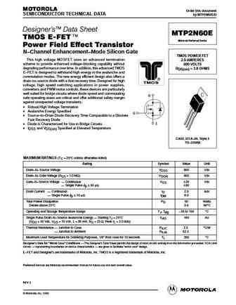
MOTOROLA Order this document SEMICONDUCTOR TECHNICAL DATA by MTP2N60E/D Designer's Data Sheet MTP2N60E TMOS E-FET. Motorola Preferred Device Power Field Effect Transistor N Channel Enhancement Mode Silicon Gate TMOS POWER FET This high voltage MOSFET uses an advanced termination 2.0 AMPERES scheme to provide enhanced voltage blocking capability without 600 VOLTS degra
2n6055 2n6056.pdf
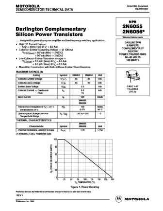
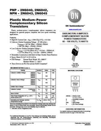
Order this document MOTOROLA by 2N6055/D SEMICONDUCTOR TECHNICAL DATA NPN 2N6055 Darlington Complementary 2N6056* Silicon Power Transistors *Motorola Preferred Device . . . designed for general purpose amplifier and low frequency switching applications. DARLINGTON High DC Current Gain 8 AMPERE hFE = 3000 (Typ) @ IC = 4.0 Adc COMPLEMENTARY Collector Emitter Sustai
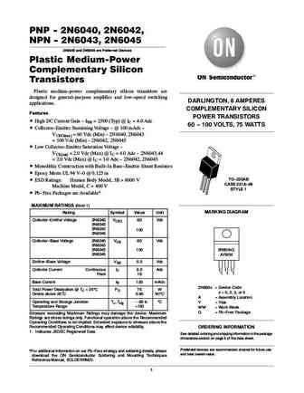
2n6040 2n6041 2n6042 2n6043 2n6044 2n6045.pdf
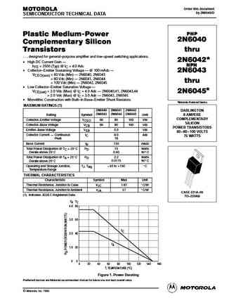
Order this document MOTOROLA by 2N6040/D SEMICONDUCTOR TECHNICAL DATA PNP Plastic Medium-Power 2N6040 Complementary Silicon Transistors thru . . . designed for general purpose amplifier and low speed switching applications. * 2N6042 High DC Current Gain NPN hFE = 2500 (Typ) @ IC = 4.0 Adc Collector Emitter Sustaining Voltage @ 100 mAdc 2N6043 VCEO(sus
2n6050 2n6051 2n6052 2n6057 2n6058 2n6059.pdf
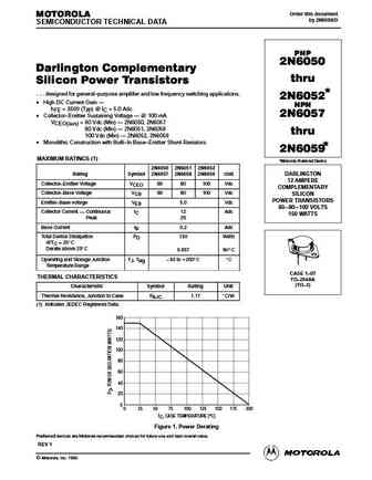
Order this document MOTOROLA by 2N6050/D SEMICONDUCTOR TECHNICAL DATA PNP 2N6050 Darlington Complementary thru Silicon Power Transistors . . . designed for general purpose amplifier and low frequency switching applications. 2N6052* High DC Current Gain NPN hFE = 3500 (Typ) @ IC = 5.0 Adc Collector Emitter Sustaining Voltage @ 100 mA 2N6057 VCEO(sus) = 60 Vdc (
mtp1n100 mtp1n55 mtp1n95 mtp20p06 mtp2955 mtp2n55 mtp2n60 mtp2n85 mtp2p45 mtp2p50 mtp3n100 mtp3n75 mtp3n80 mtp3n95 mtp3p25 mtp4n85.pdf
2n6071 2n6073 2n6075 .pdf
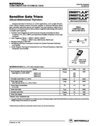
MOTOROLA Order this document SEMICONDUCTOR TECHNICAL DATA by 2N6071/D * 2N6071,A,B * 2N6073,A,B Sensitive Gate Triacs 2N6075,A,B* Silicon Bidirectional Thyristors *Motorola preferred devices . . . designed primarily for full-wave ac control applications, such as light dimmers, motor controls, heating controls and power supplies; or wherever full-wave silicon TRIACs gate controlle
2n5630 2n6030 2n5631 2n6031.pdf
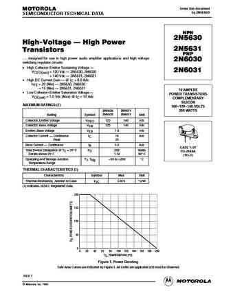
Order this document MOTOROLA by 2N5630/D SEMICONDUCTOR TECHNICAL DATA NPN 2N5630 High-Voltage High Power 2N5631 Transistors PNP . . . designed for use in high power audio amplifier applications and high voltage 2N6030 switching regulator circuits. High Collector Emitter Sustaining Voltage 2N6031 VCEO(sus) = 120 Vdc 2N5630, 2N6030 VCEO(sus) = 140 Vdc 2N5631, 2N603
irf22n60c.pdf
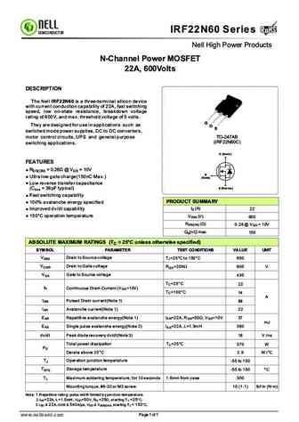
RoHS IRF22N60 Series RoHS SEMICONDUCTOR Nell High Power Products N-Channel Power MOSFET 22A, 600Volts DESCRIPTION The Nell IRF22N60 is a three-terminal silicon device with current conduction capability of 22A, fast switching speed, low on-state resistance, breakdown voltage rating of 600V, and max. threshold voltage of 5 volts. G They are designed for use in applications such as
irfp22n60c3pbf.pdf
PD - 95005 SMPS MOSFET IRFP22N60C3PbF Superjunction Power MOSFET AppIications l PFC and Primary Switch in SMPS l Uninterruptible Power Supply VDSS@TJ max RDS(on) typ. ID l High Speed Power Switching l Hard Switched and High Frequency Circuits 650V 155m 22A l Lead-Free Benefits D l Ultra Low Gate Charge Qg results in Simple Drive Requirement l Improved Gate, Avalanche and Dy
irfp22n60k.pdf
PD - 94414 IRFP22N60K SMPS MOSFET HEXFET Power MOSFET Applications VDSS RDS(on) typ. ID l Hard Switching Primary or PFS Switch 600V 240m 22A l Switch Mode Power Supply (SMPS) l Uninterruptible Power Supply l High Speed Power Switching l Motor Drive Benefits l Low Gate Charge Qg results in Simple Drive Requirement l Improved Gate, Avalanche and Dynamic dv/dt Ruggedness l Full
php2n60e phb2n60e phd2n60e.pdf
Philips Semiconductors Product specification PowerMOS transistors PHP2N60E, PHB2N60E, PHD2N60E Avalanche energy rated FEATURES SYMBOL QUICK REFERENCE DATA d Repetitive Avalanche Rated Fast switching VDSS = 600 V Stable off-state characteristics High thermal cycling performance ID = 1.9 A g Low thermal resistance RDS(ON) 6 s GENERAL DESCRIPTION N-chan
php2n60e 3.pdf

Philips Semiconductors Product specification PowerMOS transistors PHP2N60E, PHB2N60E, PHD2N60E Avalanche energy rated FEATURES SYMBOL QUICK REFERENCE DATA d Repetitive Avalanche Rated Fast switching VDSS = 600 V Stable off-state characteristics High thermal cycling performance ID = 1.9 A g Low thermal resistance RDS(ON) 6 s GENERAL DESCRIPTION N-chan
php2n60 1.pdf
Philips Semiconductors Product specification -------------------------------------------------------------------------------------------------------------- PowerMOS transistor PHP2N60 ---------------------------------------------------------------------------------------------------------------------------------------------------------- GENERAL DESCRIPTION QUICK REFERENCE DATA N-channel
phx2n60e 3.pdf
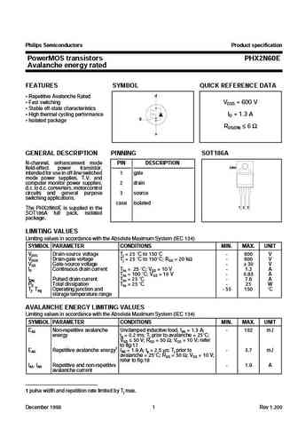
Philips Semiconductors Product specification PowerMOS transistors PHX2N60E Avalanche energy rated FEATURES SYMBOL QUICK REFERENCE DATA d Repetitive Avalanche Rated Fast switching VDSS = 600 V Stable off-state characteristics High thermal cycling performance ID = 1.3 A g Isolated package RDS(ON) 6 s GENERAL DESCRIPTION PINNING SOT186A N-channel, enhan
2n6059.pdf
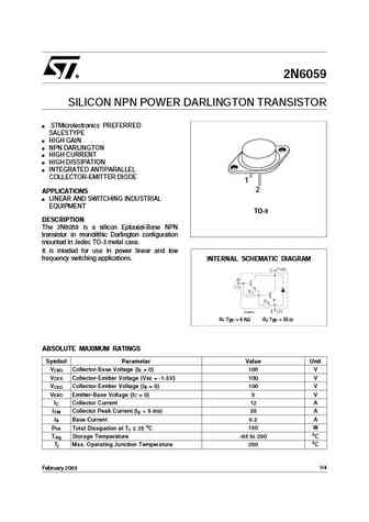
2N6059 SILICON NPN POWER DARLINGTON TRANSISTOR STMicrolectronics PREFERRED SALESTYPE HIGH GAIN NPN DARLINGTON HIGH CURRENT HIGH DISSIPATION INTEGRATED ANTIPARALLEL COLLECTOR-EMITTER DIODE 1 2 APPLICATIONS LINEAR AND SWITCHING INDUSTRIAL EQUIPMENT TO-3 DESCRIPTION The 2N6059 is a silicon Epitaxial-Base NPN transistor in monolithic Darlington configuration mount
stp12n60m2.pdf
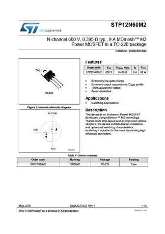
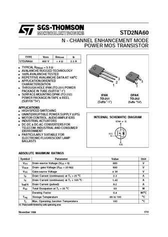
STP12N60M2 N-channel 600 V, 0.395 typ., 9 A MDmesh M2 Power MOSFET in a TO-220 package Datasheet - production data Features Order code V R max. I P DS DS(on) D TOT STP12N60M2 600 V 0.450 9 A 85 W Extremely low gate charge Excellent output capacitance (COSS) profile 100% avalanche tested Zener-protected Applications Switching applications F
stk2n60.pdf
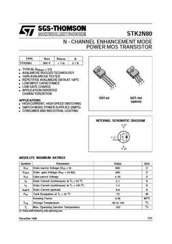
STK2N80 N - CHANNEL ENHANCEMENT MODE POWER MOS TRANSISTOR TYPE V R I DSS DS(on) D STK2N80 800 V
std12n60dm2ag.pdf
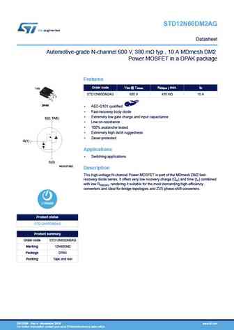
STD12N60DM2AG Datasheet Automotive-grade N-channel 600 V, 380 m typ., 10 A MDmesh DM2 Power MOSFET in a DPAK package Features VDS @ TJmax RDS(on ) max. ID Order code TAB STD12N60DM2AG 650 V 430 m 10 A 3 2 1 DPAK AEC-Q101 qualified Fast-recovery body diode Extremely low gate charge and input capacitance D(2, TAB) Low on-resistance 100% avalanche test
stfi12n60m2.pdf
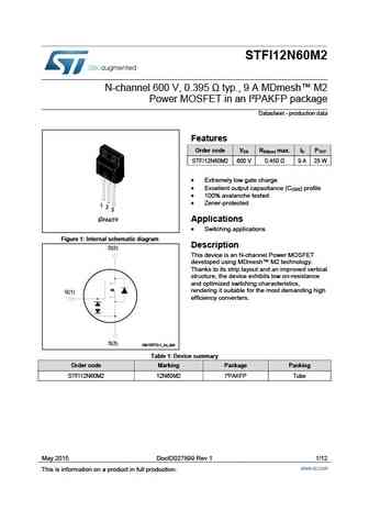
STFI12N60M2 N-channel 600 V, 0.395 typ., 9 A MDmesh M2 Power MOSFET in an I PAKFP package Datasheet - production data Features Order code V R max. I P DS DS(on) D TOT STFI12N60M2 600 V 0.450 9 A 25 W Extremely low gate charge Excellent output capacitance (COSS) profile 100% avalanche tested Zener-protected Applications Switching application
stk2n60-.pdf
STK2NA60 N - CHANNEL ENHANCEMENT MODE FAST POWER MOS TRANSISTOR TYPE V R I DSS DS(on) D STK2NA60 600 V
stp2n60.pdf
STP2N60 STP2N60FI N - CHANNEL ENHANCEMENT MODE POWER MOS TRANSISTOR TYPE VDSS RDS(on) ID STP2N60 600 V
sdt2n60.pdf
STD2NA60 N - CHANNEL ENHANCEMENT MODE POWER MOS TRANSISTOR TYPE V R I DSS DS(on) D STD2NA60 600 V
stf12n60m2.pdf
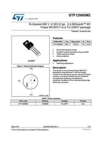
STF12N60M2 N-channel 600 V, 0.395 typ., 9 A MDmesh M2 Power MOSFET in a TO-220FP package Datasheet - production data Features Order code V R max. I P DS DS(on) D TOT STF12N60M2 600 V 0.450 9 A 25 W Extremely low gate charge Excellent output capacitance (COSS) profile 3 100% avalanche tested 2 Zener-protected 1 Applications TO-220FP Switch
stu12n60m2.pdf
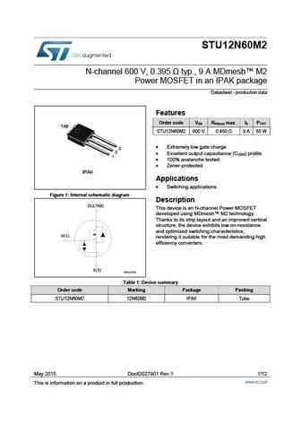
STU12N60M2 N-channel 600 V, 0.395 typ., 9 A MDmesh M2 Power MOSFET in an IPAK package Datasheet - production data Features Order code V R max. I P DS DS(on) D TOT TAB STU12N60M2 600 V 0.450 9 A 85 W Extremely low gate charge 3 2 Excellent output capacitance (COSS) profile 1 100% avalanche tested Zener-protected IPAK Applications Switchi
stl12n60m2.pdf
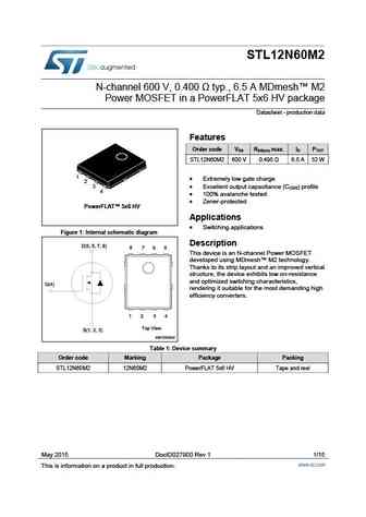
STL12N60M2 N-channel 600 V, 0.400 typ., 6.5 A MDmesh M2 Power MOSFET in a PowerFLAT 5x6 HV package Datasheet - production data Features Order code V R max. I P DS DS(on) D TOT STL12N60M2 600 V 0.495 6.5 A 52 W 1 Extremely low gate charge 2 3 Excellent output capacitance (COSS) profile 4 100% avalanche tested Zener-protected PowerFLAT 5x6 HV
2n6036 2n6039.pdf
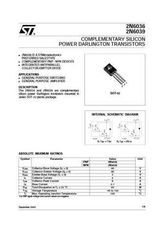
2N6036 2N6039 COMPLEMENTARY SILICON POWER DARLINGTON TRANSISTORS 2N6036 IS A STMicroelectronics PREFERRED SALESTYPE COMPLEMENTARY PNP - NPN DEVICES INTEGRATED ANTIPARALLEL COLLECTOR-EMITTER DIODE APPLICATIONS GENERAL PURPOSE SWITCHING GENERAL PURPOSE AMPLIFIER 1 2 3 DESCRIPTION The 2N6036 and 2N6039 are complementary SOT-32 silicon power Darlington transistors
tk62n60w.pdf

TK62N60W MOSFETs Silicon N-Channel MOS (DTMOS ) TK62N60W TK62N60W TK62N60W TK62N60W 1. Applications 1. Applications 1. Applications 1. Applications Switching Voltage Regulators 2. Features 2. Features 2. Features 2. Features (1) Low drain-source on-resistance RDS(ON) = 0.033 (typ.) by used to Super Junction Structure DTMOS (2) Easy to control Gate switching (3) E
tk62n60w5.pdf
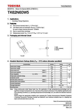
TK62N60W5 MOSFETs Silicon N-Channel MOS (DTMOS ) TK62N60W5 TK62N60W5 TK62N60W5 TK62N60W5 1. Applications 1. Applications 1. Applications 1. Applications Switching Voltage Regulators 2. Features 2. Features 2. Features 2. Features (1) Fast reverse recovery time trr = 170 ns (typ.) (2) Low drain-source on-resistance RDS(ON) = 0.036 (typ.) by used to Super Junction St
tk62n60x.pdf
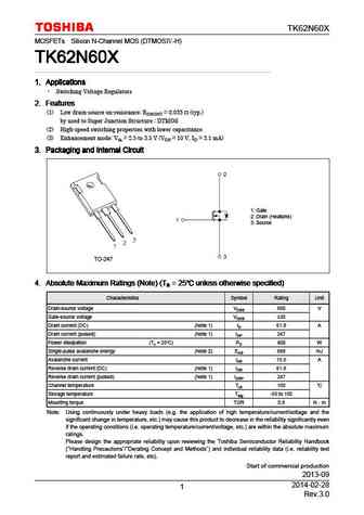
TK62N60X MOSFETs Silicon N-Channel MOS (DTMOS -H) TK62N60X TK62N60X TK62N60X TK62N60X 1. Applications 1. Applications 1. Applications 1. Applications Switching Voltage Regulators 2. Features 2. Features 2. Features 2. Features (1) Low drain-source on-resistance RDS(ON) = 0.033 (typ.) by used to Super Junction Structure DTMOS (2) High-speed switching properties wit
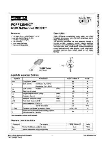
fqp2n60.pdf

April 2006 QFET FQP2N60C/FQPF2N60C 2.0A, 600V N-Channel MOSFET General Description Features These N-Channel enhancement mode power field effect rDS(on) = 4.7 @ VGS = 10 V transistors are produced using Fairchild s proprietary, Low gate charge (typical 8.5 nC) planar stripe, DMOS technology. Low Crss (typical 4.3 pF) This advanced technology has been especially tailo
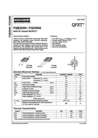
fqb12n60tm am002 fqi12n60tu.pdf
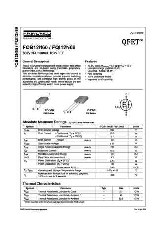
April 2000 TM QFET QFET QFET QFET FQB12N60 / FQI12N60 600V N-Channel MOSFET General Description Features These N-Channel enhancement mode power field effect 10.5A, 600V, RDS(on) = 0.7 @ VGS = 10 V transistors are produced using Fairchild s proprietary, Low gate charge ( typical 42 nC) planar stripe, DMOS technology. Low Crss ( typical 25 pF) This advanced technolo
fqa12n60.pdf
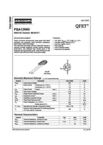
April 2000 TM QFET QFET QFET QFET FQA12N60 600V N-Channel MOSFET General Description Features These N-Channel enhancement mode power field effect 12A, 600V, RDS(on) = 0.7 @ VGS = 10 V transistors are produced using Fairchild s proprietary, Low gate charge ( typical 42 nC) planar stripe, DMOS technology. Low Crss ( typical 25 pF) This advanced technology has been e
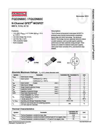
fqd2n60c fqu2n60c fqu2n60ctu.pdf
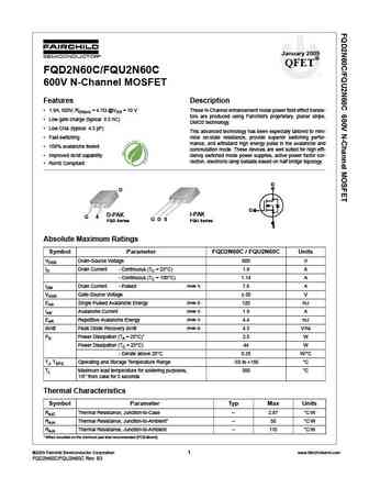
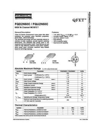
January 2009 QFET FQD2N60C/FQU2N60C 600V N-Channel MOSFET Features Description 1.9A, 600V, RDS(on) = 4.7 @VGS = 10 V These N-Channel enhancement mode power field effect transis- tors are produced using Fairchild s proprietary, planar stripe, Low gate charge (typical 8.5 nC) DMOS technology. Low Crss (typical 4.3 pF) This advanced technology has been especially tail
hgtg12n60a4d hgtp12n60a4d hgt1s12n60a4d.pdf
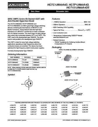
HGTG12N60A4D, HGTP12N60A4D, HGT1S12N60A4DS Data Sheet December 2001 600V, SMPS Series N-Channel IGBT with Features Anti-Parallel Hyperfast Diode >100kHz Operation . . . . . . . . . . . . . . . . . . . . . 390V, 12A The HGTG12N60A4D, HGTP12N60A4D and 200kHz Operation . . . . . . . . . . . . . . . . . . . . . . . 390V, 9A HGT1S12N60A4DS are MOS gated high voltage switching
2n6076.pdf
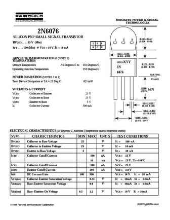
DISCRETE POWER & SIGNAL TECHNOLOGIES 2N6076 SILICON PNP SMALL SIGNAL TRANSISTOR 0.135 - 0.145 1 2 3 (3.429 - 3.683) BVCEO . . . . 25 V (Min) 1 2 3 B C E hFE . . . . 100 (Min) @ VCE = 10 V, IC = 10 mA 0.175 - 0.185 (4.450 - 4.700) ABSOLUTE MAXIMUM RATINGS (NOTE 1) TEMPERATURES LOGOXYY 0.175 - 0.185 Storage Temperature -55 Degrees C to 150 Degrees C (4.450 - 4.700) 2N Op
fqpf12n60.pdf

April 2000 TM QFET QFET QFET QFET FQPF12N60 600V N-Channel MOSFET General Description Features These N-Channel enhancement mode power field effect 5.8A, 600V, RDS(on) = 0.7 @ VGS = 10 V transistors are produced using Fairchild s proprietary, Low gate charge ( typical 42 nC) planar stripe, DMOS technology. Low Crss ( typical 25 pF) This advanced technology has been
ssr2n60b ssu2n60b.pdf

November 2001 SSR2N60B / SSU2N60B 600V N-Channel MOSFET General Description Features These N-Channel enhancement mode power field effect 1.8A, 600V, RDS(on) = 5.0 @VGS = 10 V transistors are produced using Fairchild s proprietary, Low gate charge ( typical 12.5 nC) planar, DMOS technology. Low Crss ( typical 7.6 pF) This advanced technology has been especially tailored
fqb12n60ctm fqi12n60ctu.pdf
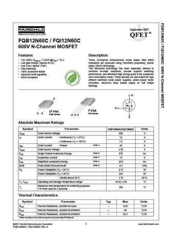
September 2007 QFET FQB12N60C / FQI12N60C 600V N-Channel MOSFET Features Description 12A, 600V, RDS(on) = 0.65 @VGS = 10 V These N-Channel enhancement mode power field effect Low gate charge ( typical 48 nC) transistors are produced using Fairchild s proprietary, planar stripe, DMOS technology. Low Crss ( typical 21pF) This advanced technology has been especially
fch072n60.pdf
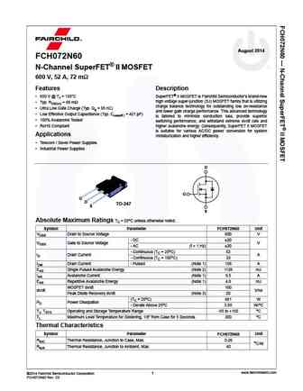
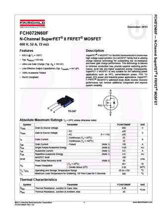
August 2014 FCH072N60 N-Channel SuperFET II MOSFET 600 V, 52 A, 72 m Features Description 650 V @ TJ = 150 C SuperFET II MOSFET is Fairchild Semiconductor s brand-new high voltage super-junction (SJ) MOSFET family that is utilizing Typ. RDS(on) = 66 m charge balance technology for outstanding low on-resistance Ultra Low Gate Charge (Typ. Qg = 95 nC) and lower
fqb2n60tm.pdf
April 2000 TM QFET QFET QFET QFET FQB2N60 / FQI2N60 600V N-Channel MOSFET General Description Features These N-Channel enhancement mode power field effect 2.4A, 600V, RDS(on) = 4.7 @VGS = 10 V transistors are produced using Fairchild s proprietary, Low gate charge ( typical 9.0 nC) planar stripe, DMOS technology. Low Crss ( typical 5.0 pF) This advanced technology
fqaf12n60.pdf
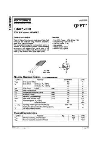
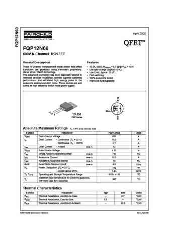
April 2000 TM QFET QFET QFET QFET FQAF12N60 600V N-Channel MOSFET General Description Features These N-Channel enhancement mode power field effect 7.8A, 600V, RDS(on) = 0.7 @ VGS = 10 V transistors are produced using Fairchild s proprietary, Low gate charge ( typical 42 nC) planar stripe, DMOS technology. Low Crss ( typical 25 pF) This advanced technology has been
fqp12n60.pdf
April 2000 TM QFET QFET QFET QFET FQP12N60 600V N-Channel MOSFET General Description Features These N-Channel enhancement mode power field effect 10.5A, 600V, RDS(on) = 0.7 @ VGS = 10 V transistors are produced using Fairchild s proprietary, Low gate charge ( typical 42 nC) planar stripe, DMOS technology. Low Crss ( typical 25 pF) This advanced technology has been
fqp2n60c fqpf2n60c.pdf
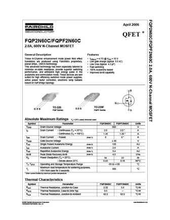
April 2006 QFET FQP2N60C/FQPF2N60C 2.0A, 600V N-Channel MOSFET General Description Features These N-Channel enhancement mode power field effect rDS(on) = 4.7 @ VGS = 10 V transistors are produced using Fairchild s proprietary, Low gate charge (typical 8.5 nC) planar stripe, DMOS technology. Low Crss (typical 4.3 pF) This advanced technology has been especially tailo
fqpf2n60.pdf
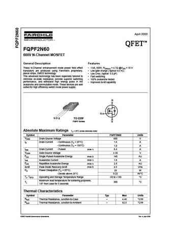
April 2000 TM QFET QFET QFET QFET FQPF2N60 600V N-Channel MOSFET General Description Features These N-Channel enhancement mode power field effect 1.6A, 600V, RDS(on) = 4.7 @VGS = 10 V transistors are produced using Fairchild s proprietary, Low gate charge ( typical 9.0 nC) planar stripe, DMOS technology. Low Crss ( typical 5.0 pF) This advanced technology has been
fcp22n60n fcpf22n60nt.pdf
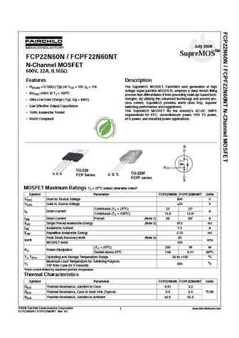
July 2009 SupreMOS TM FCP22N60N / FCPF22N60NT tm N-Channel MOSFET 600V, 22A, 0.165 Features Description RDS(on) = 0.140 ( Typ.)@ VGS = 10V, ID = 11A The SupreMOS MOSFET, Fairchild s next generation of high voltage super-junction MOSFETs, employs a deep trench filling BVDSS>650V @ TJ = 150oC process that differentiates it from preceding multi-epi based tech- nologies.
fqp12n60c.pdf
March 2014 FQP12N60C N-Channel QFET MOSFET 600 V, 12 A, 650 m Description Features These N-Channel enhancement mode power field effect 12 A, 600 V, RDS(on) = 650 m (Max.) @ VGS = 10 V, transistors are produced using Fairchild s proprietary, planar ID = 6 A stripe, DMOS technology. This advanced technology has Low Gate Charge (Typ. 48 nC) been especially tailored to
ssp2n60b sss2n60b.pdf
SSP2N60B/SSS2N60B 600V N-Channel MOSFET General Description Features These N-Channel enhancement mode power field effect 2.0A, 600V, RDS(on) = 5.0 @VGS = 10 V transistors are produced using Fairchild s proprietary, Low gate charge ( typical 12.5 nC) planar, DMOS technology. Low Crss ( typical 7.6 pF) This advanced technology has been especially tailored to Fast swit
hgtg12n60a4 hgtp12n60a4 hgt1s12n60a4.pdf
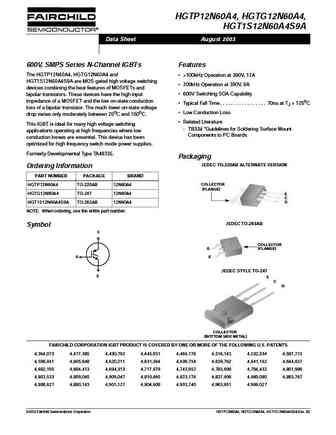
HGTP12N60A4, HGTG12N60A4, HGT1S12N60A4S9A Data Sheet August 2003 600V, SMPS Series N-Channel IGBTs Features The HGTP12N60A4, HGTG12N60A4 and >100kHz Operation at 390V, 12A HGT1S12N60A4S9A are MOS gated high voltage switching 200kHz Operation at 390V, 9A devices combining the best features of MOSFETs and 600V Switching SOA Capability bipolar transistors. These devices ha
hgtp12n60c3 hgt1s12n60c3.pdf
HGTP12N60C3, HGT1S12N60C3S Data Sheet December 2001 24A, 600V, UFS Series N-Channel IGBTs Features The HGTP12N60C3 and HGT1S12N60C3S are MOS gated 24A, 600V at TC = 25oC high voltage switching devices combining the best features 600V Switching SOA Capability of MOSFETs and bipolar transistors. These devices have the Typical Fall Time. . . . . . . . . . . . . . . . 230ns a
hgtg12n60c3d.pdf
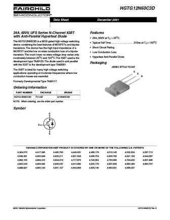
HGTG12N60C3D Data Sheet December 2001 24A, 600V, UFS Series N-Channel IGBT Features with Anti-Parallel Hyperfast Diode 24A, 600V at TC = 25oC The HGTG12N60C3D is a MOS gated high voltage switching Typical Fall Time. . . . . . . . . . . . . . . . 210ns at TJ = 150oC device combining the best features of MOSFETs and bipolar Short Circuit Rating transistors. The device has t
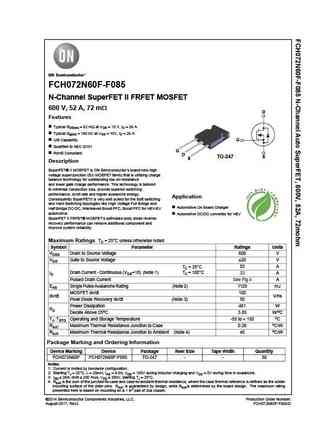
fch072n60f.pdf
December 2013 FCH072N60F N-Channel SuperFET II FRFET MOSFET 600 V, 52 A, 72 m Features Description 650 V @ TJ = 150 C SuperFET II MOSFET is Fairchild Semiconductor s brand-new high voltage super-junction (SJ) MOSFET family that is utilizing Typ. RDS(on) = 65 m charge balance technology for outstanding low on-resistance and lower gate charge performance. This techno
fdp12n60nz fdpf12n60nz.pdf
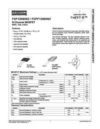
September 2010 UniFET-II TM FDP12N60NZ / FDPF12N60NZ N-Channel MOSFET 600V, 12A, 0.65 Features Description RDS(on) = 0.53 ( Typ.)@ VGS = 10V, ID = 6A These N-Channel enhancement mode power field effect transis- tors are produced using Fairchild s proprietary, planar stripe, Low gate charge ( Typ. 26nC) DOMS technology. Low Crss ( Typ. 12pF) This advance techno
fca22n60n.pdf
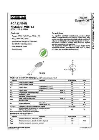
July 2009 SupreMOS TM FCA22N60N tm N-Channel MOSFET 600V, 22A, 0.165 Features Description RDS(on) = 0.140 ( Typ.)@ VGS = 10V, ID = 11A The SupreMOS MOSFET, Fairchild s next generation of high voltage super-junction MOSFETs, employs a deep trench filling BVDSS>650V @ TJ = 150oC process that differentiates it from preceding multi-epi based tech- nologies. By utilizing
ssi2n60b ssi2n60b ssw2n60b.pdf

November 2001 SSW2N60B / SSI2N60B 600V N-Channel MOSFET General Description Features These N-Channel enhancement mode power field effect 2.0A, 600V, RDS(on) = 5.0 @VGS = 10 V transistors are produced using Fairchild s proprietary, Low gate charge ( typical 12.5 nC) planar, DMOS technology. Low Crss ( typical 7.6 pF) This advanced technology has been especially tailored
ssw2n60b ssi2n60b.pdf
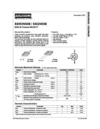
November 2001 SSW2N60B / SSI2N60B 600V N-Channel MOSFET General Description Features These N-Channel enhancement mode power field effect 2.0A, 600V, RDS(on) = 5.0 @VGS = 10 V transistors are produced using Fairchild s proprietary, Low gate charge ( typical 12.5 nC) planar, DMOS technology. Low Crss ( typical 7.6 pF) This advanced technology has been especially tailored
fqpf12n60c.pdf

November 2013 FQPF12N60C N-Channel QFET MOSFET 600 V, 12 A, 650 m Description Features These N-Channel enhancement mode power field effect 12 A, 600 V, RDS(on) = 650 m (Max.) @ VGS = 10 V, transistors are produced using Fairchild s proprietary, planar ID = 6 A stripe, DMOS technology. This advanced technology has Low Gate Charge (Typ. 48 nC) been especially tailored
fch22n60n.pdf
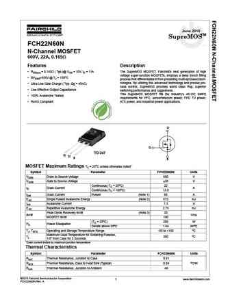
June 2010 TM SupreMOS FCH22N60N tm N-Channel MOSFET 600V, 22A, 0.165 Features Description RDS(on) = 0.140 ( Typ.)@ VGS = 10V, ID = 11A The SupreMOS MOSFET, Fairchild s next generation of high voltage super-junction MOSFETs, employs a deep trench filling BVDSS>650V @ TJ = 150oC process that differentiates it from preceding multi-epi based tech- nologies. By utilizin
fqpf12n60ct.pdf
September 2006 QFET FQPF12N60CT 600V N-Channel MOSFET Features Description 12A, 600V, RDS(on) = 0.65 @VGS = 10 V These N-Channel enhancement mode power field effect Low gate charge ( typical 48 nC) transistors are produced using Fairchild s proprietary, planar stripe, DMOS technology. Low Crss ( typical 21 pF) This advanced technology has been especially tailored
fqp12n60c fqpf12n60c.pdf
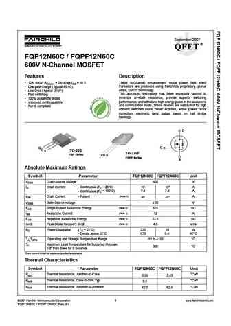
September 2007 QFET FQP12N60C / FQPF12N60C 600V N-Channel MOSFET Features Description 12A, 600V, RDS(on) = 0.65 @VGS = 10 V These N-Channel enhancement mode power field effect Low gate charge ( typical 48 nC) transistors are produced using Fairchild s proprietary, planar stripe, DMOS technology. Low Crss ( typical 21pF) This advanced technology has been especiall
fch072n60f f085.pdf
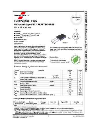
November 2014 FCH072N60F_F085 N-Channel SuperFET II FRFET MOSFET 600 V, 52 A, 72 m D Features Typical RDS(on) = 62 m at VGS = 10 V, ID = 26 A Typical Qg(tot) = 160 nC at VGS = 10V, ID = 26 A UIS Capability G Qualified to AEC Q101 G RoHS Compliant D TO-247 S S Description SuperFET II MOSFET is Fairchild Semiconductor s brand-new For current package drawing,
hgtp12n60c3d hgt1s12n60c3d.pdf
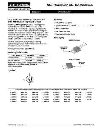
HGTP12N60C3D, HGT1S12N60C3DS Data Sheet December 2001 24A, 600V, UFS Series N-Channel IGBT Features with Anti-Parallel Hyperfast Diodes 24A, 600V at TC = 25oC This family of MOS gated high voltage switching devices Typical Fall Time at TJ = 150oC . . . . . . . . . . . . . . . . 210ns combine the best features of MOSFETs and bipolar Short Circuit Rating transistors. The
fqd2n60tf fqd2n60tm fqu2n60tu.pdf
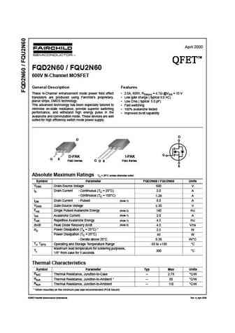
April 2000 TM QFET QFET QFET QFET FQD2N60 / FQU2N60 600V N-Channel MOSFET General Description Features These N-Channel enhancement mode power field effect 2.0A, 600V, RDS(on) = 4.7 @VGS = 10 V transistors are produced using Fairchild s proprietary, Low gate charge ( typical 9.0 nC) planar stripe, DMOS technology. Low Crss ( typical 5.0 pF) This advanced technology
fqpf12n60 fqpf12n60t.pdf
April 2000 TM QFET QFET QFET QFET FQPF12N60 600V N-Channel MOSFET General Description Features These N-Channel enhancement mode power field effect 5.8A, 600V, RDS(on) = 0.7 @ VGS = 10 V transistors are produced using Fairchild s proprietary, Low gate charge ( typical 42 nC) planar stripe, DMOS technology. Low Crss ( typical 25 pF) This advanced technology has been
fqd2n60ctm.pdf
November 2013 FQD2N60C / FQU2N60C N-Channel QFET MOSFET 600 V, 1.9 A, 4.7 Features Description 1.9 A, 600 V, RDS(on) = 4.7 (Max.) @ VGS = 10 V, This N-Channel enhancement mode power MOSFET is ID = 0.95 A produced using Fairchild Semiconductor s proprietary Low Gate Charge (Typ. 8.5 nC) planar stripe and DMOS technology. This advanced Low Crss (Typ. 4.3 pF)
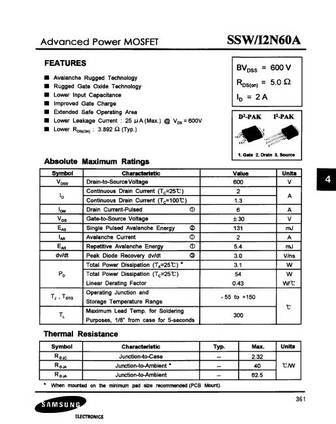
ssr2n60a.pdf
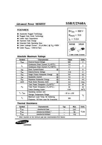
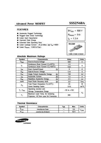
Advanced Power MOSFET FEATURES BVDSS = 600 V Avalanche Rugged Technology RDS(on) = 5 Rugged Gate Oxide Technology Lower Input Capacitance ID = 1.8 A Improved Gate Charge Extended Safe Operating Area Lower Leakage Current 25 A (Max.) @ VDS = 600V Lower RDS(ON) 3.892 (Typ.) 2 1 1 2 3 3 1. Gate 2. Drain 3. Source Absolute Maximum Ratings Symbol Charac
sss2n60a.pdf
Advanced Power MOSFET FEATURES BVDSS = 600 V Avalanche Rugged Technology RDS(on) = 5 Rugged Gate Oxide Technology Lower Input Capacitance ID = 1.3 A Improved Gate Charge Extended Safe Operating Area Lower Leakage Current 25 A (Max.) @ VDS = 600V Lower RDS(ON) 3.892 (Typ.) 1 2 3 1.Gate 2. Drain 3. Source Absolute Maximum Ratings Symbol Characteristic Valu
ssw2n60a.pdf
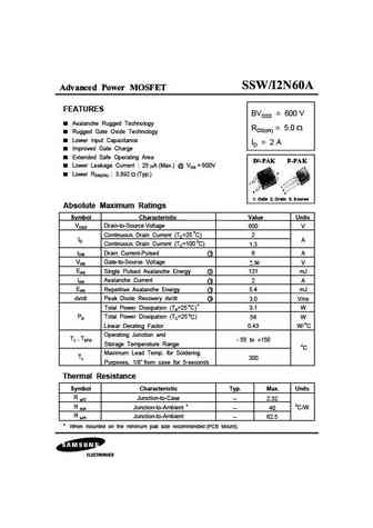
Advanced Power MOSFET FEATURES BVDSS = 600 V Avalanche Rugged Technology RDS(on) = 5.0 Rugged Gate Oxide Technology Lower Input Capacitance ID = 2 A Improved Gate Charge Extended Safe Operating Area Lower Leakage Current 25 A (Max.) @ VDS = 600V 2 Lower RDS(ON) 3.892 (Typ.) 1 1 2 3 3 1. Gate 2. Drain 3. Source Absolute Maximum Ratings Symbol Chara
sgr2n60ufd.pdf
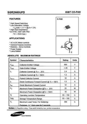
IGBT CO-PAK SGR2N60UFD FEATURES D-PAK * High Speed Switching * Low Saturation Voltage VCE(sat) = 2.1 V (@ Ic=1.2A) * High Input Impedance *CO-PAK, IGBT with FRD Trr = 45nS (typ.) APPLICATIONS C * AC & DC Motor controls * General Purpose Inverters G * Robotics , Servo Controls * Power Supply * Lamp Ballast E ABSOLUTE MAXIMUM RATINGS Symbol Rating Units Characteris
ssp2n60a.pdf
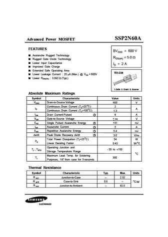
Advanced Power MOSFET FEATURES BVDSS = 600 V Avalanche Rugged Technology RDS(on) = 5.0 Rugged Gate Oxide Technology Lower Input Capacitance ID = 2 A Improved Gate Charge Extended Safe Operating Area Lower Leakage Current 25 A (Max.) @ VDS = 600V Lower RDS(ON) 3.892 (Typ.) 1 2 3 1.Gate 2. Drain 3. Source Absolute Maximum Ratings Symbol Characteristic Valu
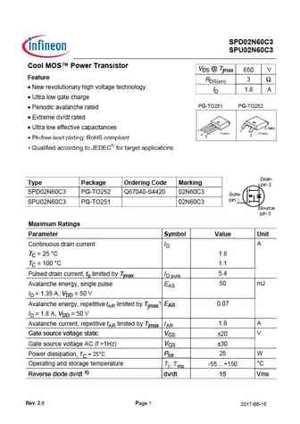
spd02n60.pdf
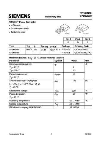
SPD02N60 SPU02N60 Preliminary data SIPMOS Power Transistor N-Channel Enhancement mode Avalanche rated Pin 1 Pin 2 Pin 3 G D S Type VDS ID RDS(on) @ VGS Package Ordering Code SPD02N60 600 V 2 A VGS = 10 V P-TO252 Q67040-S4133 5.5 SPU02N60 P-TO251 Q67040-S4127-A2 Maximum Ratings, at Tj = 25 C, unless otherwise specified Parameter Symbol Value Unit Continuous d
rdd022n60.pdf
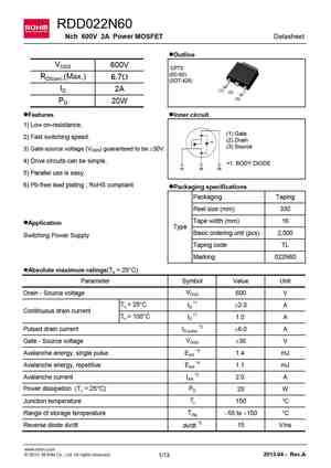
RDD022N60 Nch 600V 2A Power MOSFET Datasheet lOutline VDSS 600V CPT3 (SC-63) RDS(on) (Max.) 6.7W (SOT-428) ID 2A (1) (2) (3) PD 20W lFeatures lInner circuit 1) Low on-resistance. (1) Gate 2) Fast switching speed. (2) Drain (3) Source 3) Gate-source voltage (VGSS) guaranteed to be 30V. 4) Drive circuits can be simple. *1 BODY DIODE 5) Parallel use is easy.
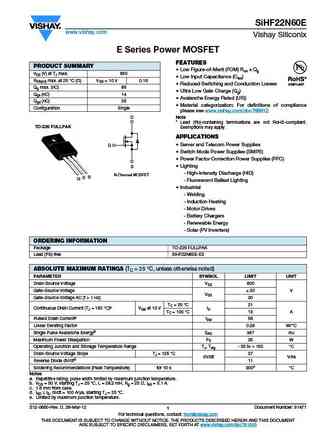
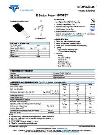
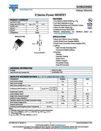
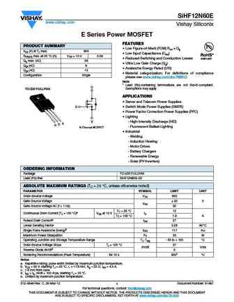
sihg22n60e.pdf
SiHG22N60E www.vishay.com Vishay Siliconix E Series Power MOSFET FEATURES PPRODUCT SUMMARY Low figure-of-merit (FOM) Ron x Qg VDS (V) at TJ max. 650 Low input capacitance (Ciss) RDS(on) max. at 25 C ( ) VGS = 10 V 0.18 Reduced switching and conduction losses Qg max. (nC) 86 Ultra low gate charge (Qg) Qgs (nC) 11 Available Avalanche energy rated (UIS) Qgd (
siha22n60ael.pdf
SiHA22N60AEL www.vishay.com Vishay Siliconix EL Series Power MOSFET FEATURES D Thin-Lead TO-220 FULLPAK Low figure-of-merit (FOM) Ron x Qg Low input capacitance (Ciss) Reduced switching and conduction losses G Ultra low gate charge (Qg) Avalanche energy rated (UIS) Material categorization for definitions of compliance S please see www.vishay.com/doc?999
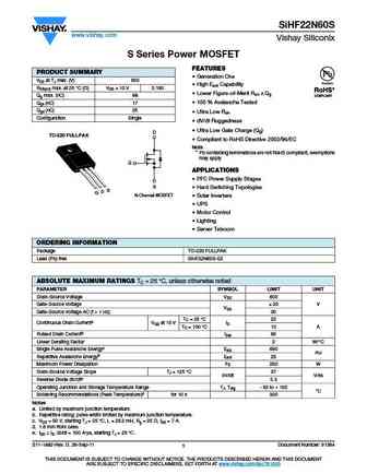
sihf22n60e.pdf
SiHF22N60E www.vishay.com Vishay Siliconix E Series Power MOSFET FEATURES PRODUCT SUMMARY Low Figure-of-Merit (FOM) Ron x Qg VDS (V) at TJ max. 650 Low Input Capacitance (Ciss) RDS(on) max. at 25 C ( ) VGS = 10 V 0.18 Reduced Switching and Conduction Losses Qg max. (nC) 86 Ultra Low Gate Charge (Qg) Qgs (nC) 14 Avalanche Energy Rated (UIS) Qgd (nC) 26
irfp22n60k sihfp22n60k.pdf
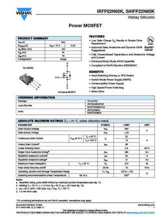
IRFP22N60K, SiHFP22N60K Vishay Siliconix Power MOSFET FEATURES PRODUCT SUMMARY Low Gate Charge Qg Results in Simple Drive VDS (V) 600 Requirement Available RDS(on) ( )VGS = 10 V 0.24 Improved Gate, Avalanche and Dynamic dV/dt RoHS* Qg (Max.) (nC) 150 COMPLIANT Ruggedness Qgs (nC) 45 Fully Characterized Capacitance and Avalanche Voltage Qgd (nC) 76 and Current Co
siha22n60e.pdf
SiHA22N60E www.vishay.com Vishay Siliconix E Series Power MOSFET FEATURES PRODUCT SUMMARY Low figure-of-merit (FOM) Ron x Qg VDS (V) at TJ max. 650 Low input capacitance (Ciss) RDS(on) max. at 25 C ( ) VGS = 10 V 0.18 Reduced switching and conduction losses Qg max. (nC) 86 Ultra low gate charge (Qg) Qgs (nC) 11 Avalanche energy rated (UIS) Qgd (nC) 24
irfp22n60k irfp22n60kpbf sihfp22n60k.pdf

IRFP22N60K, SiHFP22N60K Vishay Siliconix Power MOSFET FEATURES PRODUCT SUMMARY Low Gate Charge Qg Results in Simple Drive VDS (V) 600 Requirement Available RDS(on) ( )VGS = 10 V 0.24 Improved Gate, Avalanche and Dynamic dV/dt RoHS* Qg (Max.) (nC) 150 COMPLIANT Ruggedness Qgs (nC) 45 Fully Characterized Capacitance and Avalanche Voltage Qgd (nC) 76 and Current Co
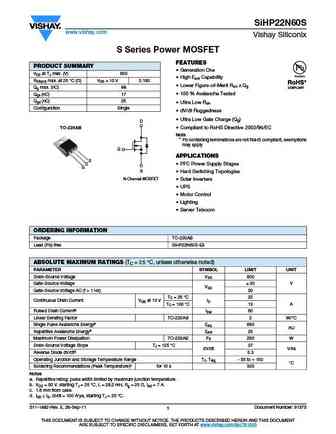
sihg22n60s.pdf
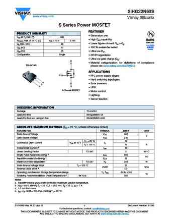
SiHG22N60S www.vishay.com Vishay Siliconix S Series Power MOSFET FEATURES PRODUCT SUMMARY Generation one VDS at TJ max. (V) 650 High EAR capability RDS(on) max. at 25 C ( ) VGS = 10 V 0.190 Lower figure-of-merit Ron x Qg Qg max. (nC) 98 100 % avalanche tested Qgs (nC) 17 Available Qgd (nC) 25 Ultra low Ron Configuration Single dV/dt ruggedness U
siha12n60e.pdf
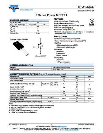
SiHA12N60E www.vishay.com Vishay Siliconix E Series Power MOSFET FEATURES PRODUCT SUMMARY Low figure-of-merit (FOM) Ron x Qg VDS (V) at TJ max. 650 Low input capacitance (Ciss) RDS(on) max. at 25 C ( ) VGS = 10 V 0.38 Reduced switching and conduction losses Qg max. (nC) 58 Ultra low gate charge (Qg) Qgs (nC) 6 Avalanche energy rated (UIS) Qgd (nC) 13 M
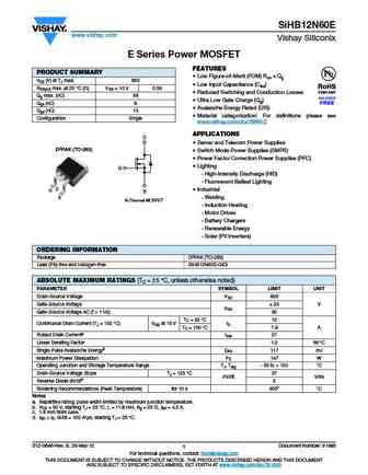
sihp12n60e.pdf
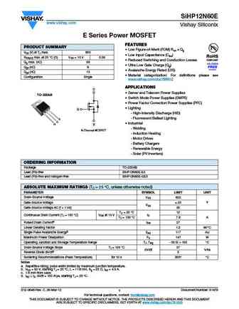
SiHP12N60E www.vishay.com Vishay Siliconix E Series Power MOSFET FEATURES PRODUCT SUMMARY Low Figure-of-Merit (FOM) Ron x Qg VDS (V) at TJ max. 650 Low Input Capacitance (Ciss) RDS(on) max. at 25 C ( ) VGS = 10 V 0.38 Reduced Switching and Conduction Losses Qg max. (nC) 58 Ultra Low Gate Charge (Qg) Qgs (nC) 6 Avalanche Energy Rated (UIS) Qgd (nC) 13
sihf22n60s.pdf
SiHF22N60S www.vishay.com Vishay Siliconix S Series Power MOSFET FEATURES PRODUCT SUMMARY Generation One VDS at TJ max. (V) 650 High EAR Capability RDS(on) max. at 25 C ( ) VGS = 10 V 0.190 Lower Figure-of-Merit Ron x Qg Qg max. (nC) 98 100 % Avalanche Tested Qgs (nC) 17 Qgd (nC) 25 Ultra Low Ron Configuration Single dV/dt Ruggedness Ultra Low G
sihp22n60e.pdf
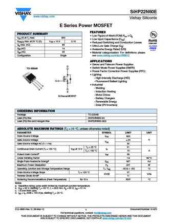
SiHP22N60E www.vishay.com Vishay Siliconix E Series Power MOSFET FEATURES PRODUCT SUMMARY Low Figure-of-Merit (FOM) Ron x Qg VDS (V) at TJ max. 650 Low Input Capacitance (Ciss) RDS(on) max. at 25 C ( ) VGS = 10 V 0.18 Reduced Switching and Conduction Losses Qg max. (nC) 86 Ultra Low Gate Charge (Qg) Qgs (nC) 14 Avalanche Energy Rated (UIS) Qgd (nC) 26
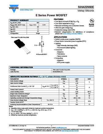
siha22n60ae.pdf
SiHA22N60AE www.vishay.com Vishay Siliconix E Series Power MOSFET FEATURES D Thin-Lead TO-220 FULLPAK Low figure-of-merit (FOM) Ron x Qg Low input capacitance (Ciss) Reduced switching and conduction losses G Ultra low gate charge (Qg) Available Avalanche energy rated (UIS) Material categorization for definitions of compliance S please see www.vishay.co
sihp22n60s.pdf
SiHP22N60S www.vishay.com Vishay Siliconix S Series Power MOSFET FEATURES PRODUCT SUMMARY Generation One VDS at TJ max. (V) 650 High EAR Capability RDS(on) max. at 25 C ( ) VGS = 10 V 0.190 Lower Figure-of-Merit Ron x Qg Qg max. (nC) 98 100 % Avalanche Tested Qgs (nC) 17 Qgd (nC) 25 Ultra Low Ron Configuration Single dV/dt Ruggedness Ultra Low G
sihb22n60s.pdf
SiHB22N60S www.vishay.com Vishay Siliconix S Series Power MOSFET FEATURES PRODUCT SUMMARY Generation One VDS at TJ max. (V) 650 Halogen-free According to IEC 61249-2-21 RDS(on) max. at 25 C ( ) VGS = 10 V 0.190 Definition Qg max. (nC) 98 High EAR Capability Qgs (nC) 17 Lower Figure-of-Merit Ron x Qg Qgd (nC) 25 100 % Avalanche Tested Configuration Single
sihb22n60e.pdf
SiHB22N60E www.vishay.com Vishay Siliconix E Series Power MOSFET FEATURES PRODUCT SUMMARY Low Figure-of-Merit (FOM) Ron x Qg VDS (V) at TJ max. 650 Low Input Capacitance (Ciss) RDS(on) max. at 25 C ( ) VGS = 10 V 0.18 Reduced Switching and Conduction Losses Qg max. (nC) 86 Ultra Low Gate Charge (Qg) Qgs (nC) 14 Avalanche Energy Rated (UIS) Qgd (nC) 26
sihf12n60e.pdf
SiHF12N60E www.vishay.com Vishay Siliconix E Series Power MOSFET FEATURES PRODUCT SUMMARY Low Figure-of-Merit (FOM) Ron x Qg VDS (V) at TJ max. 650 Low Input Capacitance (Ciss) RDS(on) max. at 25 C ( ) VGS = 10 V 0.38 Reduced Switching and Conduction Losses Qg max. (nC) 58 Ultra Low Gate Charge (Qg) Qgs (nC) 6 Avalanche Energy Rated (UIS) Qgd (nC) 13
sihb12n60e.pdf
SiHB12N60E www.vishay.com Vishay Siliconix E Series Power MOSFET FEATURES PRODUCT SUMMARY Low Figure-of-Merit (FOM) Ron x Qg VDS (V) at TJ max. 650 Low Input Capacitance (Ciss) RDS(on) max. at 25 C ( ) VGS = 10 V 0.38 Reduced Switching and Conduction Losses Qg max. (nC) 58 Ultra Low Gate Charge (Qg) Qgs (nC) 6 Avalanche Energy Rated (UIS) Qgd (nC) 13
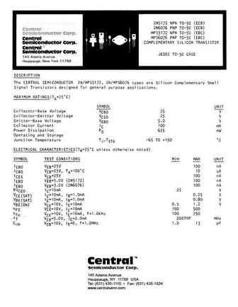
2n5172 2n6076 mps5172 mps6076.pdf
TM Central Semiconductor Corp. 145 Adams Avenue Hauppauge, NY 11788 USA Tel (631) 435-1110 Fax (631) 435-1824 www.centralsemi.com
2n5629 2n5630 2n6029 2n6030.pdf
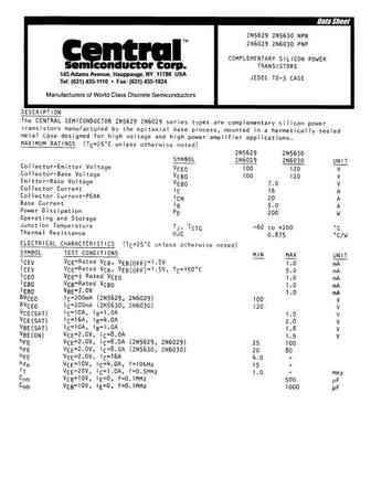
145 Adams Avenue, Hauppauge, NY 11788 USA Tel (631) 435-1110 Fax (631) 435-1824
skb02n60g.pdf

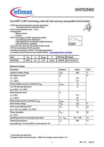
SKB02N60 Fast IGBT in NPT-technology with soft, fast recovery anti-parallel EmCon diode C 75% lower Eoff compared to previous generation combined with low conduction losses Short circuit withstand time 10 s G E Designed for frequency inverters for washing machines, fans, pumps and vacuum cleaners NPT-Technology for 600V applications offers - very tight
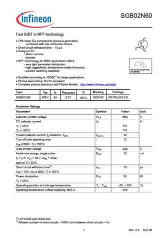

sgp02n60.pdf

SGP02N60 SGD02N60 Fast IGBT in NPT-technology C 75% lower Eoff compared to previous generation combined with low conduction losses Short circuit withstand time 10 s G E Designed for - Motor controls - Inverter NPT-Technology for 600V applications offers - very tight parameter distribution - high ruggedness, temperature stable behaviour PG-TO-
skp02n60.pdf
SKP02N60 Fast IGBT in NPT-technology with soft, fast recovery anti-parallel EmCon diode C 75% lower Eoff compared to previous generation combined with low conduction losses Short circuit withstand time 10 s G E Designed for - Motor controls - Inverter NPT-Technology for 600V applications offers - very tight parameter distribution - high ruggednes
skb02n60.pdf
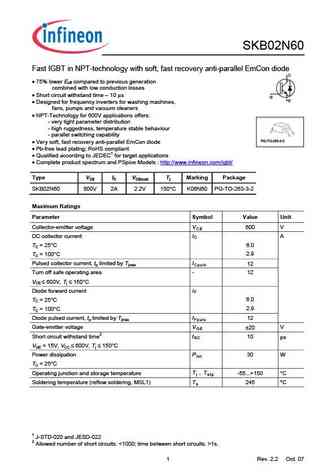
SKB02N60 Fast IGBT in NPT-technology with soft, fast recovery anti-parallel EmCon diode C 75% lower Eoff compared to previous generation combined with low conduction losses Short circuit withstand time 10 s G E Designed for frequency inverters for washing machines, fans, pumps and vacuum cleaners NPT-Technology for 600V applications offers - very tight
sgp02n60 sgd02n60g.pdf

SGP02N60 SGD02N60 Fast IGBT in NPT-technology C 75% lower Eoff compared to previous generation combined with low conduction losses Short circuit withstand time 10 s G E Designed for - Motor controls - Inverter NPT-Technology for 600V applications offers - very tight parameter distribution - high ruggedness, temperature stable behaviour PG-TO-
spp02n60s5.pdf
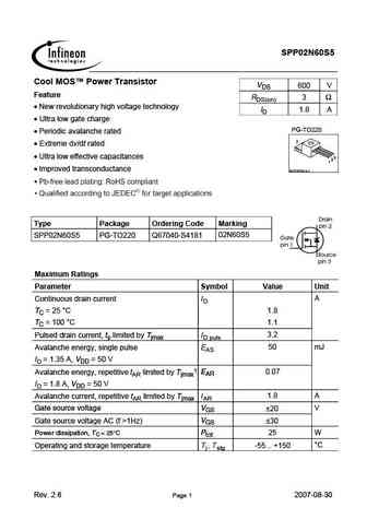
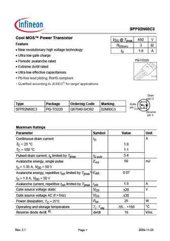
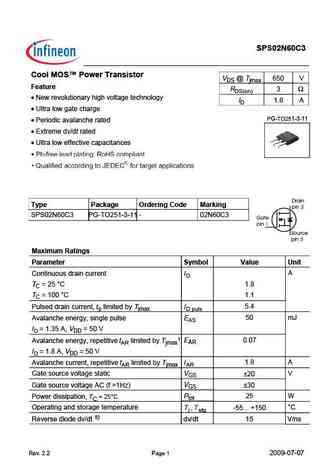
SPP02N60S5 Cool MOS Power Transistor VDS 600 V Feature RDS(on) 3 New revolutionary high voltage technology ID 1.8 A Ultra low gate charge PG-TO220 Periodic avalanche rated 2 Extreme dv/dt rated Ultra low effective capacitances 3 2 1 Improved transconductance P-TO220-3-1 Type Package Ordering Code Marking 02N60S5 SPP02N60S5 PG-TO220 Q67040-S418
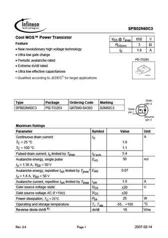
spn02n60c3.pdf
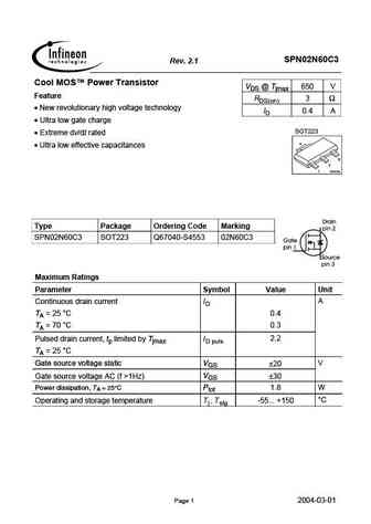
SPN02N60C3 Rev. 2.1 Cool MOS Power Transistor VDS @ Tjmax 650 V Feature RDS(on) 3 New revolutionary high voltage technology ID 0.4 A Ultra low gate charge SOT223 Extreme dv/dt rated 4 Ultra low effective capacitances 3 2 1 VPS05163 Type Package Ordering Code Marking SPN02N60C3 SOT223 Q67040-S4553 02N60C3 Maximum Ratings Parameter Symbol Value Unit A C
spu02n60s5 spd02n60s5.pdf
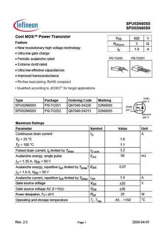
SPU02N60S5 SPD02N60S5 Cool MOS Power Transistor VDS 600 V Feature RDS(on) 3 New revolutionary high voltage technology ID 1.8 A Ultra low gate charge PG-TO252 PG-TO251 Periodic avalanche rated Extreme dv/dt rated 2 3 Ultra low effective capacitances 3 1 2 1 Improved transconductance Type Package Ordering Code Marking 02N60S5 SPU02N60S5 PG-TO2
spd02n60s5 spu02n60s5.pdf

SPU02N60S5 SPD02N60S5 Cool MOS Power Transistor VDS 600 V Feature RDS(on) 3 New revolutionary high voltage technology ID 1.8 A Ultra low gate charge PG-TO252 PG-TO251 Periodic avalanche rated Extreme dv/dt rated 2 3 Ultra low effective capacitances 3 1 2 1 Improved transconductance Type Package Ordering Code Marking 02N60S5 SPU02N60S5 PG-TO2
spb02n60s5.pdf
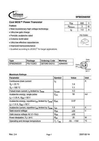
SPB02N60S5 Cool MOS Power Transistor VDS 600 V Feature RDS(on) 3 New revolutionary high voltage technology ID 1.8 A Ultra low gate charge PG-TO263 Periodic avalanche rated Extreme dv/dt rated Ultra low effective capacitances Improved transconductance Type Package Ordering Code Marking SPB02N60S5 PG-TO263 Q67040-S4212 02N60S5 Maximum Ratings Parame
sgp02n60 sgd02n60.pdf
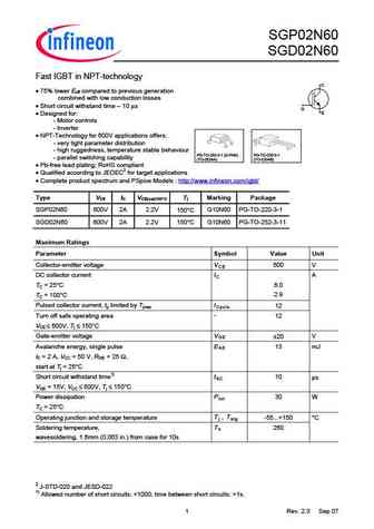
SGP02N60 SGD02N60 Fast IGBT in NPT-technology C 75% lower Eoff compared to previous generation combined with low conduction losses Short circuit withstand time 10 s G E Designed for - Motor controls - Inverter NPT-Technology for 600V applications offers - very tight parameter distribution - high ruggedness, temperature stable behaviour PG-TO-
sgd02n60.pdf

SGP02N60 SGD02N60 Fast IGBT in NPT-technology C 75% lower Eoff compared to previous generation combined with low conduction losses Short circuit withstand time 10 s G E Designed for - Motor controls - Inverter NPT-Technology for 600V applications offers - very tight parameter distribution - high ruggedness, temperature stable behaviour PG-TO-
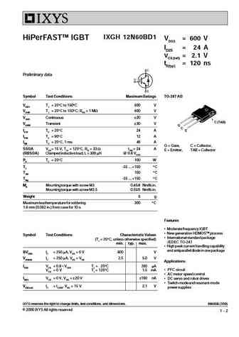
ixga12n60cd1 ixgp12n60cd1.pdf
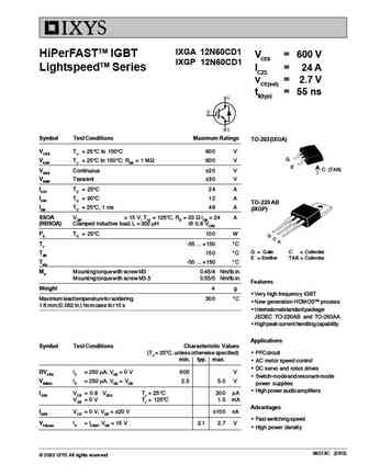
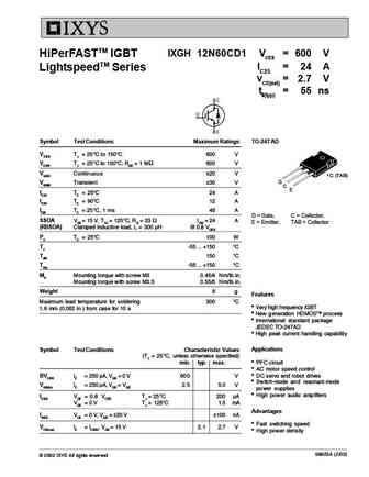
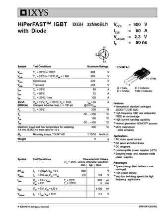
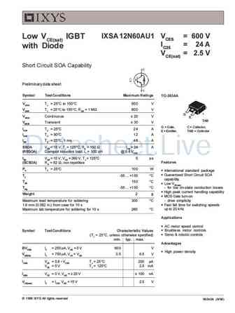
IXGA 12N60CD1 HiPerFASTTM IGBT VCES = 600 V IXGP 12N60CD1 LightspeedTM Series IC25 = 24 A VCE(sat) = 2.7 V tfi(typ) = 55 ns Symbol Test Conditions Maximum Ratings TO-263 (IXGA) VCES TJ = 25 C to 150 C 600 V G VCGR TJ = 25 C to 150 C; RGE = 1 M 600 V E C (TAB) VGES Continuous 20 V VGEM Transient 30 V IC25 TC = 25 C24 A IC90 TC = 90 C12 A TO-220 AB ICM TC = 25 C,
ixsn62n60u1.pdf
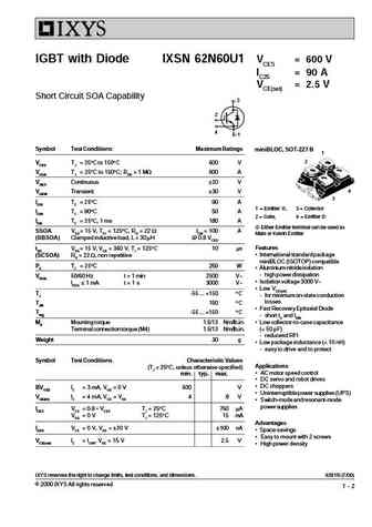
IGBT with Diode IXSN 62N60U1 VCES = 600 V IC25 = 90 A VCE(sat) = 2.5 V Short Circuit SOA Capability 3 2 4 1 Symbol Test Conditions Maximum Ratings miniBLOC, SOT-227 B 1 2 VCES TJ = 25 C to 150 C 600 V VCGR TJ = 25 C to 150 C; RGE = 1 MW 600 A VGES Continuous 20 V 4 VGEM Transient 30 V 3 IC25 TC = 25 C90 A 1 = Emitter , 3 = Collector IC90 TC = 90 C50 A 2 = Gate, 4
ixsn52n60au1.pdf
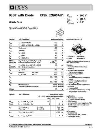
IGBT with Diode IXSN 52N60AU1 VCES = 600 V IC25 = 80 A Combi Pack VCE(sat) = 3 V 3 Short Circuit SOA Capability 2 4 1 Symbol Test Conditions Maximum Ratings miniBLOC, SOT-227 B 1 VCES TJ = 25 C to 150 C 600 V 2 VCGR TJ = 25 C to 150 C; RGE = 1 MW 600 A VGES Continuous 20 V VGEM Transient 30 V 4 IC25 TC = 25 C80 A 3 IC90 TC = 90 C40 A 1 = Emitter , 3 = Collector IC
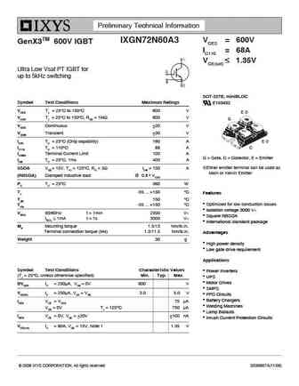
ixgt72n60b3.pdf

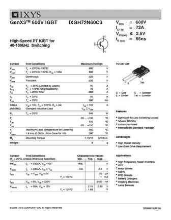
GenX3TM B3-Class VCES = 600V IXGH72N60B3 IC110 = 72A IGBTs IXGT72N60B3 VCE(sat) 1.80V tfi(typ) = 90ns Medium Speed low Vsat PT IGBTs 5-40 kHz Switching TO-247 AD (IXGH) Symbol Test Conditions Maximum Ratings VCES TJ = 25 C to 150 C 600 V VCGR TJ = 25 C to 150 C, RGE = 1M 600 V G VGES Continuous 20 V C (TAB) E VGEM Transient 30 V IC25 TC = 2
ixga12n60b ixgp12n60b.pdf

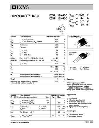
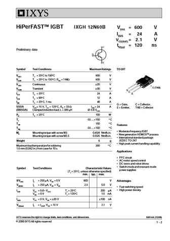
IXGA 12N60B VCES = 600 V HiPerFASTTM IGBT IXGP 12N60B IC25 = 24 A VCE(sat) = 2.1 V tfi(typ) = 120 ns Preliminary data sheet Symbol Test Conditions Maximum Ratings TO-220 AB (IXGP) VCES TJ = 25 C to 150 C 600 V VCGR TJ = 25 C to 150 C; RGE = 1 M 600 V C (TAB) VGES Continuous 20 V G E VGEM Transient 30 V IC25 TC = 25 C24 A IC90 TC = 90 C12 A TO-263 AA (IXGA) ICM TC =
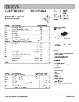
ixgh72n60a3.pdf
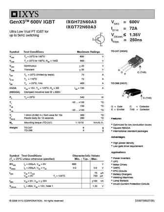
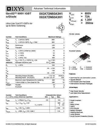
IXGH72N60A3 VCES = 600V GenX3TM 600V IGBT IXGT72N60A3 IC110 = 72A Ultra Low Vsat PT IGBT for VCE(sat) 1.35V up to 5kHz switching tfi(typ) = 250ns TO-247 (IXGH) Symbol Test Conditions Maximum Ratings VCES TC = 25 C to 150 C 600 V VCGR TJ = 25 C to 150 C, RGE = 1M 600 V VGES Continuous 20 V VGEM Transient 30 V G C C (TAB) E IC25 TC = 25 C (lim
ixgp12n60c.pdf

VCES = 600 V IXGA 12N60C HiPerFASTTM IGBT IC25 = 24 A IXGP 12N60C VCE(sat)= 2.7 V tfi(typ) = 55 ns Symbol Test Conditions Maximum Ratings TO-263 AA (IXGA) VCES TJ = 25 C to 150 C 600 V VCGR TJ = 25 C to 150 C; RGE = 1 M 600 V G VGES Continuous 20 V C (tab) E VGEM Transient 30 V IC25 TC = 25 C24 A TO-220 AB IC90 TC = 90 C12 A (IXGP) ICM TC = 25 C, 1 ms 48
ixgx72n60c3h1.pdf
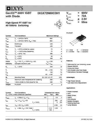
VCES = 600V GenX3TM 600V IGBT IXGX72N60C3H1 IC110 = 72A with Diode VCE(sat) 2.5V tfi(typ) = 55ns High-Speed PT IGBT for 40-100kHz Switching PLUS247 Symbol Test Conditions Maximum Ratings VCES TJ = 25 C to 150 C 600 V VCGR TJ = 25 C to 150 C, RGE = 1M 600 V G G D VGES Continuous 20 V C ES Tab VGEM Transient 30 V IC25 TC = 25 C (Limited by L
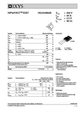
ixgt32n60c.pdf
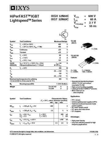
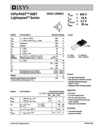
IXGH 32N60C VCES = 600 V HiPerFASTTM IGBT IXGT 32N60C IC25 = 60 A LightspeedTM Series VCE(sat)typ = 2.1 V tfi typ = 55 ns TO-268 Symbol Test Conditions Maximum Ratings (IXGT) VCES TJ = 25 C to 150 C 600 V VCGR TJ = 25 C to 150 C; RGE = 1 MW 600 V G E C (TAB) VGES Continuous 20 V VGEM Transient 30 V IC25 TC = 25 C60 A TO-247 AD (IXGH) IC110 TC = 110 C32 A ICM TC =
ixgt32n60bd1.pdf

IXGH 32N60B HiPerFASTTM IGBT VCES = 600 V IXGT 32N60B IC25 = 60 A IXGH 32N60BD1 VCE(sat) = 2.3 V IXGT 32N60BD1 tfi(typ) = 85 ns (D1) Symbol Test Conditions Maximum Ratings TO-268 (IXGT) G VCES TJ = 25 C to 150 C 600 V E C VCGR TJ = 25 C to 150 C; RGE = 1 M 600 V (TAB) VGES Continuous 20 V TO-247 AD VGEM Transient 30 V (IXGH) IC25 TC = 25 C60 A IC90 TC = 90 C3
ixgr32n60cd1.pdf
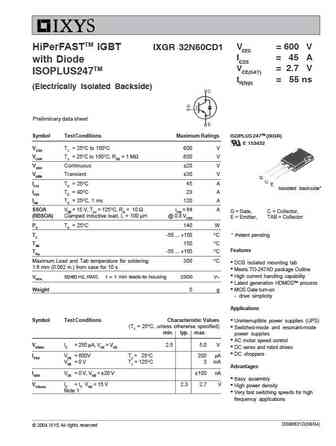
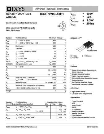
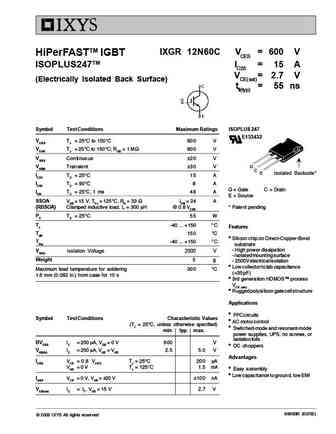
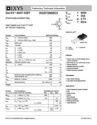
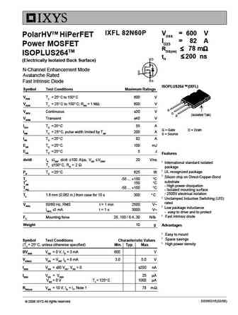
VCES = 600 V HiPerFASTTM IGBT IXGR 32N60CD1 IC25 = 45 A with Diode VCE(SAT) = 2.7 V ISOPLUS247TM tfi(typ) = 55 ns (Electrically Isolated Backside) Preliminary data sheet Symbol Test Conditions Maximum Ratings ISOPLUS 247TM (IXGR) E 153432 VCES TJ = 25 C to 150 C 600 V VCGR TJ = 25 C to 150 C; RGE = 1 M 600 V VGES Continuous 20 V VGEM Transient 30 V G C IC25 TC = 25
ixgt32n60cd1.pdf

IXGH 32N60CD1 VCES = 600 V HiPerFASTTM IGBT IXGT 32N60CD1 IC25 = 60 A with Diode VCE(SAT)typ = 2.1 V tfi(typ) = 55 ns Light Speed Series TO-247 AD (IXGH) Symbol Test Conditions Maximum Ratings VCES TJ = 25 C to 150 C 600 V VCGR TJ = 25 C to 150 C; RGE = 1 M 600 V G VGES Continuous 20 V C (TAB) C VGEM Transient 30 V E IC25 TC = 25 C60 A IC90 TC = 90 C32 A TO-268 (D
ixgr72n60c3d1.pdf
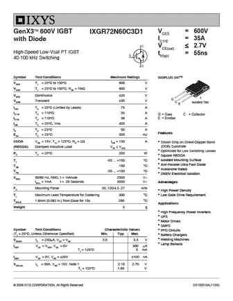
TM VCES = 600V GenX3 600V IGBT IXGR72N60C3D1 IC110 = 35A with Diode VCE(sat) 2.7V High-Speed Low-Vsat PT IGBT tfi(typ) = 55ns 40-100 kHz Switching Symbol Test Conditions Maximum Ratings ISOPLUS 247TM VCES TJ = 25 C to 150 C 600 V VCGR TJ = 25 C to 150 C, RGE = 1M 600 V VGES Continuous 20 V G VGEM Transient 30 V C Isolated Tab E IC25 TC = 25
ixfk32n60 ixfn32n60 ixfk36n60 ixfn36n60.pdf
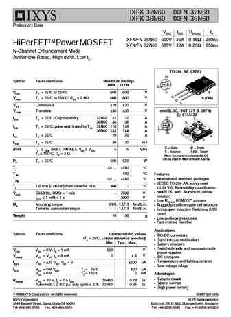
IXFK 32N60 IXFN 32N60 IXFK 36N60 IXFN 36N60 Preliminary Data VDSS ID25 RDS(on) trr IXFK/FN 36N60 600V 36A 0.18 250ns HiPerFETTM Power MOSFET IXFK/FN 32N60 600V 32A 0.25 250ns N-Channel Enhancement Mode Avalanche Rated, High dv/dt, Low trr TO-264 AA (IXFK) Symbol Test Conditions Maximum Ratings IXFK IXFN VDSS TJ = 25 C to 150 C 600 600 V G VDGR TJ = 25 C to 150 C; RGS = 1
ixgh32n60au1 ixgh32n60au1s.pdf
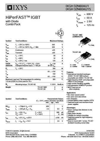
IXGH 32N60AU1 IXGH 32N60AU1S VCES = 600 V IC25 = 60 A HiPerFASTTM IGBT with Diode VCE(sat) = 2.9V Combi Pack tfi = 125 ns TO-247 SMD (32N60AU1S) Symbol Test Conditions Maximum Ratings VCES TJ = 25 C to 150 C 600 V G C (TAB) E VCGR TJ = 25 C to 150 C; RGE = 1 M 600 V VGES Continuous 20 V TO-247 AD VGEM Transient 30 V IC25 TC = 25 C60 A IC90 TC = 90 C32 A C (TAB)
ixgr72n60a3.pdf
VCES = 600V GenX3TM 600V IGBT IXGR72N60A3 IC110 = 52A VCE(sat) 1.35V Ultra-low Vsat PT IGBTs for up to 5kHz switching tfi(typ) = 250ns Symbol Test Conditions Maximum Ratings ISOPLUS247TM (IXGR) VCES TJ = 25 C to 150 C 600 V E153432 VCGR TJ = 25 C to 150 C, RGE = 1M 600 V VGES Continuous 20 V VGEM Transient 30 V IC110 TC = 110 C 52 A G ICM TC
ixgh32n60a.pdf

IXGH 32N60A IXGH 32N60AS VCES = 600 V IC25 = 60 A HiPerFASTTM IGBT VCE(sat) = 2.9 V tfi = 125 ns TO-247 SMD (32N60AS) Symbol Test Conditions Maximum Ratings C (TAB) VCES TJ = 25 C to 150 C 600 V G E VCGR TJ = 25 C to 150 C; RGE = 1 M 600 V VGES Continuous 20 V TO-247 AD VGEM Transient 30 V IC25 TC = 25 C60 A IC90 TC = 90 C32 A C (TAB) G ICM TC = 25 C, 1 ms 120
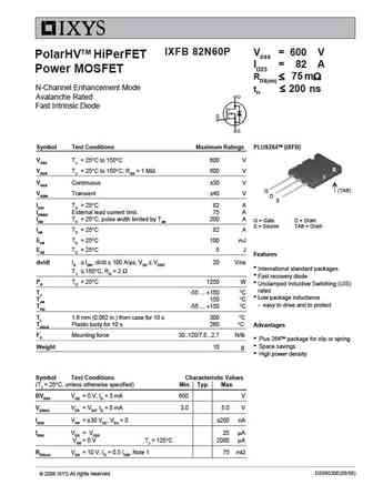
ixfa22n60p3.pdf
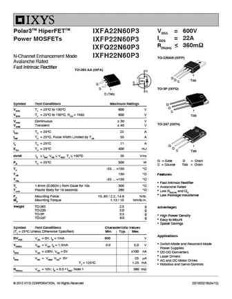
Polar3TM HiperFETTM VDSS = 600V IXFA22N60P3 ID25 = 22A Power MOSFETs IXFP22N60P3 RDS(on) 360m IXFQ22N60P3 N-Channel Enhancement Mode IXFH22N60P3 TO-220AB (IXFP) Avalanche Rated Fast Intrinsic Rectifier TO-263 AA (IXFA) G D Tab S G S TO-3P (IXFQ) D (Tab) Symbol Test Conditions Maximum Ratings G D VDSS TJ = 25 C to 150 C 600 V S VDGR
ixgp12n60cd1.pdf

IXGA 12N60CD1 HiPerFASTTM IGBT VCES = 600 V IXGP 12N60CD1 LightspeedTM Series IC25 = 24 A VCE(sat) = 2.7 V tfi(typ) = 55 ns Symbol Test Conditions Maximum Ratings TO-263 (IXGA) VCES TJ = 25 C to 150 C 600 V G VCGR TJ = 25 C to 150 C; RGE = 1 M 600 V E C (TAB) VGES Continuous 20 V VGEM Transient 30 V IC25 TC = 25 C24 A IC90 TC = 90 C12 A TO-220 AB ICM TC = 25 C,
ixgh72n60c3.pdf
VCES = 600V GenX3TM 600V IGBT IXGH72N60C3 IC110 = 72A VCE(sat) 2.5V tfi (typ) = 55ns High-Speed PT IGBT for 40-100kHz Switching Symbol Test Conditions Maximum Ratings TO-247 AD VCES TJ = 25 C to 150 C 600 V VCGR TJ = 25 C to 150 C, RGE = 1M 600 V VGES Continuous 20 V G VGEM Transient 30 V C Tab E IC25 TC = 25 C (Limited by Leads) 75 A IC
ixfh22n60p ixfv22n60p.pdf
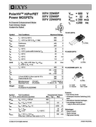
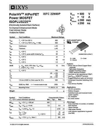
IXFH 22N60P VDSS = 600 V PolarHVTM HiPerFET IXFV 22N60P ID25 = 22 A Power MOSFETs IXFV 22N60PS RDS(on) 350 m N-Channel Enhancement Mode trr 200 ns Fast Intrinsic Diode Avalanche Rated TO-247 (IXFH) Symbol Test Conditions Maximum Ratings VDSS TJ = 25 C to 150 C 600 V VDGR TJ = 25 C to 150 C; RGS = 1 M 60
ixgh32n60c.pdf

IXGH 32N60C VCES = 600 V HiPerFASTTM IGBT IXGT 32N60C IC25 = 60 A LightspeedTM Series VCE(sat)typ = 2.1 V tfi typ = 55 ns TO-268 Symbol Test Conditions Maximum Ratings (IXGT) VCES TJ = 25 C to 150 C 600 V VCGR TJ = 25 C to 150 C; RGE = 1 MW 600 V G E C (TAB) VGES Continuous 20 V VGEM Transient 30 V IC25 TC = 25 C60 A TO-247 AD (IXGH) IC110 TC = 110 C32 A ICM TC =
ixgr72n60b3d1.pdf
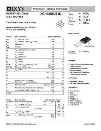
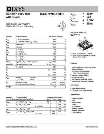
Preliminary Technical Information GenX3TM B3-Class VCES = 600V IXGR72N60B3D1 IGBT w/Diode IC110 = 40A VCE(sat) 1.80V (Electrically Isolated Back Surface) tfi(typ) = 90ns Medium Speed Low Vsat PT IGBTs for 5-40 kHz Switching ISOPLUS 247TM Symbol Test Conditions Maximum Ratings VCES TJ = 25 C to 150 C 600 V VCGR TJ = 25 C to 150 C, RGE = 1M 600 V VGES
ixgh72n60b3.pdf
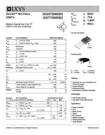
GenX3TM B3-Class VCES = 600V IXGH72N60B3 IC110 = 72A IGBTs IXGT72N60B3 VCE(sat) 1.80V tfi(typ) = 90ns Medium Speed low Vsat PT IGBTs 5-40 kHz Switching TO-247 AD (IXGH) Symbol Test Conditions Maximum Ratings VCES TJ = 25 C to 150 C 600 V VCGR TJ = 25 C to 150 C, RGE = 1M 600 V G VGES Continuous 20 V C (TAB) E VGEM Transient 30 V IC25 TC = 2
ixgh12n60cd1.pdf
HiPerFASTTM IGBT IXGH 12N60CD1 VCES = 600 V IC25 = 24 A LightspeedTM Series VCE(sat) = 2.7 V tfi(typ) = 55 ns Symbol Test Conditions Maximum Ratings TO-247 AD VCES TJ = 25 C to 150 C 600 V VCGR TJ = 25 C to 150 C; RGE = 1 M 600 V VGES Continuous 20 V C (TAB) G VGEM Transient 30 V C E IC25 TC = 25 C24 A IC90 TC = 90 C12 A ICM TC = 25 C, 1 ms 48 A G = Gate, C = Co
ixgr72n60a3h1.pdf
Advance Technical Information GenX3TM 600V IGBT VCES = 600V IXGR72N60A3H1 w/Diode IC110 = 52A VCE(sat) 1.35V (Electrically Isolated Back Surface) tfi(typ) = 250ns Ultra-Low Vsat PT IGBT for up to 5kHz Switching Symbol Test Conditions Maximum Ratings ISOPLUS 247TM VCES TJ = 25 C to 150 C 600 V VCGR TJ = 25 C to 150 C, RGE = 1M 600 V VGES Continuous
ixgt72n60a3.pdf

IXGH72N60A3 VCES = 600V GenX3TM 600V IGBT IXGT72N60A3 IC110 = 72A Ultra Low Vsat PT IGBT for VCE(sat) 1.35V up to 5kHz switching tfi(typ) = 250ns TO-247 (IXGH) Symbol Test Conditions Maximum Ratings VCES TC = 25 C to 150 C 600 V VCGR TJ = 25 C to 150 C, RGE = 1M 600 V VGES Continuous 20 V VGEM Transient 30 V G C C (TAB) E IC25 TC = 25 C (lim
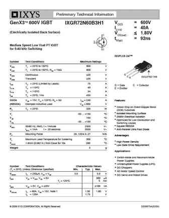
ixgh32n60cd1.pdf
IXGH 32N60CD1 VCES = 600 V HiPerFASTTM IGBT IXGT 32N60CD1 IC25 = 60 A with Diode VCE(SAT)typ = 2.1 V tfi(typ) = 55 ns Light Speed Series TO-247 AD (IXGH) Symbol Test Conditions Maximum Ratings VCES TJ = 25 C to 150 C 600 V VCGR TJ = 25 C to 150 C; RGE = 1 M 600 V G VGES Continuous 20 V C (TAB) C VGEM Transient 30 V E IC25 TC = 25 C60 A IC90 TC = 90 C32 A TO-268 (D
ixgr72n60b3h1.pdf
Preliminary Technical Information TM VCES = 600V GenX3 600V IGBT IXGR72N60B3H1 IC110 = 40A (Electrically Isolated Back Surface) VCE(sat) 1.80V tfi(typ) = 92ns Medium Speed Low Vsat PT IGBT for 5-40 kHz Switching ISOPLUS 247TM Symbol Test Conditions Maximum Ratings VCES TJ = 25 C to 150 C 600 V VCGR TJ = 25 C to 150 C, RGE = 1M 600 V G VGES Continu
ixgk72n60a3h1 ixgx72n60a3h1.pdf

Advance Technical Information GenX3TM 600V IGBT VCES = 600V IXGK72N60A3H1 w/Diode IC110 = 72A IXGX72N60A3H1 VCE(sat) 1.35V tfi(typ) = 250ns Ultra-Low Vsat PT IGBTs for up to 5kHz Switching TO-264 (IXGK) Symbol Test Conditions Maximum Ratings VCES TJ = 25 C to 150 C 600 V VCGR TJ = 25 C to 150 C, RGE = 1M 600 V (TAB) G VGES Continuous 20 V C E
ixgr12n60c.pdf
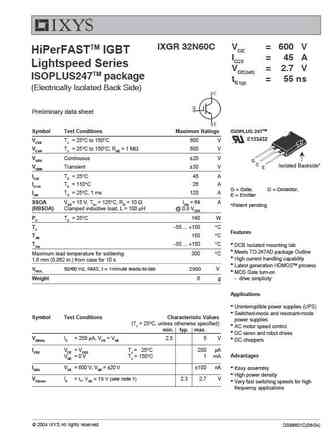
IXGR 12N60C VCES = 600 V HiPerFASTTM IGBT IC25 = 15 A ISOPLUS247TM VCE(sat)= 2.7 V (Electrically Isolated Back Surface) tfi(typ) = 55 ns Symbol Test Conditions Maximum Ratings ISOPLUS 247 E153432 VCES TJ = 25 C to 150 C 600 V VCGR TJ = 25 C to 150 C; RGE = 1 M 600 V VGES Continuous 20 V VGEM Transient 30 V G C E Isolated Backside* IC25 TC = 25 C15 A IC90 TC = 90 C
ixgn72n60c3h1.pdf
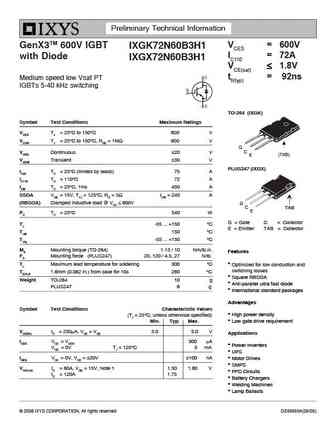
GenX3TM 600V IGBT VCES = 600V IXGN72N60C3H1 with Diode IC110 = 52A VCE(sat) 2.50V tfi(typ) = 55ns High-Speed Low-Vsat PT IGBTs 40-100 kHz Switching SOT-227B, miniBLOC E153432 Symbol Test Conditions Maximum Ratings E VCES TJ = 25 C to 150 C 600 V G VCGR TJ = 25 C to 150 C, RGE = 1M 600 V VGES Continuous 20 V VGEM Transient 30 V E IC25 TC
ixga12n60c ixgp12n60c.pdf
VCES = 600 V IXGA 12N60C HiPerFASTTM IGBT IC25 = 24 A IXGP 12N60C VCE(sat)= 2.7 V tfi(typ) = 55 ns Symbol Test Conditions Maximum Ratings TO-263 AA (IXGA) VCES TJ = 25 C to 150 C 600 V VCGR TJ = 25 C to 150 C; RGE = 1 M 600 V G VGES Continuous 20 V C (tab) E VGEM Transient 30 V IC25 TC = 25 C24 A TO-220 AB IC90 TC = 90 C12 A (IXGP) ICM TC = 25 C, 1 ms 48
ixgh32n60bd1.pdf

IXGH 32N60B HiPerFASTTM IGBT VCES = 600 V IXGT 32N60B IC25 = 60 A IXGH 32N60BD1 VCE(sat) = 2.3 V IXGT 32N60BD1 tfi(typ) = 85 ns (D1) Symbol Test Conditions Maximum Ratings TO-268 (IXGT) G VCES TJ = 25 C to 150 C 600 V E C VCGR TJ = 25 C to 150 C; RGE = 1 M 600 V (TAB) VGES Continuous 20 V TO-247 AD VGEM Transient 30 V (IXGH) IC25 TC = 25 C60 A IC90 TC = 90 C3
ixgx72n60b3h1.pdf
Preliminary Technical Information VCES = 600V GenX3TM 600V IGBT IXGK72N60B3H1 IC110 = 72A with Diode IXGX72N60B3H1 VCE(sat) 1.8V tfi(typ) = 92ns Medium speed low Vsat PT IGBTs 5-40 kHz switching TO-264 (IXGK) Symbol Test Conditions Maximum Ratings VCES TJ = 25 C to 150 C 600 V VCGR TJ = 25 C to 150 C, RGE = 1M 600 V G C VGES Continuous 20 V (
ixgr72n60c3.pdf
Preliminary Technical Information TM VCES = 600V GenX3 600V IGBT IXGR72N60C3 IC110 = 35A (Electrically Isolated Tab) VCE(sat) 2.7V tfi(typ) = 55ns High-Speed Low-Vsat PT IGBT 40-100 kHz Switching ISOPLUS 247TM Symbol Test Conditions Maximum Ratings VCES TJ = 25 C to 150 C 600 V VCGR TJ = 25 C to 150 C, RGE = 1M 600 V G C Isolated Tab VGES Co
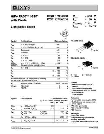
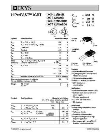
ixgh12n60c.pdf
IXGH 12N60C HiPerFASTTM IGBT VCES = 600 V LightspeedTM Series IC25 = 24 A VCE(sat) = 2.7 V tfi(typ) = 55 ns Symbol Test Conditions Maximum Ratings TO-247 VCES TJ = 25 C to 150 C 600 V VCGR TJ = 25 C to 150 C; RGE = 1 M 600 V VGES Continuous 20 V VGEM Transient 30 V C (TAB) G IC25 TC = 25 C24 A C E IC90 TC = 90 C12 A ICM TC = 25 C, 1 ms 48 A G = Gate, C = Collecto
ixgr32n60c.pdf
IXGR 32N60C VCE = 600 V HiPerFASTTM IGBT IC25 = 45 A Lightspeed Series VCE(sat) = 2.7 V ISOPLUS247TM package tfi typ = 55 ns (Electrically Isolated Back Side) Preliminary data sheet Symbol Test Conditions Maximum Ratings ISOPLUS 247TM E153432 VCES TJ = 25 C to 150 C 600 V VCGR TJ = 25 C to 150 C; RGE = 1 M 600 V VGES Continuous 20 V G C Isolated Backside* VGEM Transie
ixgt32n60b.pdf
IXGH 32N60B HiPerFASTTM IGBT VCES = 600 V IXGT 32N60B IC25 = 60 A IXGH 32N60BD1 VCE(sat) = 2.3 V IXGT 32N60BD1 tfi(typ) = 85 ns (D1) Symbol Test Conditions Maximum Ratings TO-268 (IXGT) G VCES TJ = 25 C to 150 C 600 V E C VCGR TJ = 25 C to 150 C; RGE = 1 M 600 V (TAB) VGES Continuous 20 V TO-247 AD VGEM Transient 30 V (IXGH) IC25 TC = 25 C60 A IC90 TC = 90 C3
ixgh12n60bd1.pdf
IXGH 12N60BD1 HiPerFASTTM IGBT VDSS = 600 V ID25 = 24 A VCE(sat) = 2.1 V tfi(typ) = 120 ns Preliminary data Symbol Test Conditions Maximum Ratings TO-247 AD VCES TJ = 25 C to 150 C 600 V VCGR TJ = 25 C to 150 C; RGE = 1 MW 600 V VGES Continuous 20 V C (TAB) VGEM Transient 30 V G C IC25 TC = 25 C24 A E IC90 TC = 90 C12 A ICM TC = 25 C, 1 ms 48 A G = Gate, C = Collect
ixgn72n60a3.pdf
Preliminary Technical Information VCES = 600V IXGN72N60A3 GenX3TM 600V IGBT IC110 = 68A VCE(sat) 1.35V Ultra Low Vsat PT IGBT for up to 5kHz switching E SOT-227B, miniBLOC Symbol Test Conditions Maximum Ratings E153432 VCES TJ = 25 C to 150 C 600 V E VCGR TJ = 25 C to 150 C, RGE = 1M 600 V G VGES Continuous 20 V VGEM Transient 30 V IC25 TC
ixfb82n60p.pdf
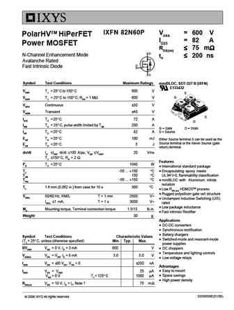
IXFB 82N60P VDSS = 600 V PolarHVTM HiPerFET ID25 = 82 A Power MOSFET RDS(on) 75 m N-Channel Enhancement Mode trr 200 ns Avalanche Rated Fast Intrinsic Diode Symbol Test Conditions Maximum Ratings PLUS264TM (IXFB) VDSS TJ = 25 C to 150 C 600 V VDGR TJ = 25 C to 150 C; RGS = 1 M 600 V VGSS Continuous 30 V (TAB) G
ixfl82n60p.pdf
IXFL 82N60P VDSS = 600 V PolarHVTM HiPerFET ID25 = 82 A Power MOSFET RDS(on) 78 m ISOPLUS264TM trr 200 ns (Electrically Isolated Back Surface) N-Channel Enhancement Mode Avalanche Rated Fast Intrinsic Diode TM ISOPLUS264 (IXFL) Symbol Test Conditions Maximum Ratings VDSS TJ = 25 C to 150 C 600 V VDGR TJ = 25
ixgh32n60bu1.pdf
IXGH 32N60BU1 VCES = 600 V HiPerFASTTM IGBT IC25 = 60 A with Diode VCE(sat) = 2.3 V tfi = 80 ns Symbol Test Conditions Maximum Ratings TO-247 AD VCES TJ = 25 C to 150 C 600 V VCGR TJ = 25 C to 150 C; RGE = 1 M 600 V C (TAB) VGES Continuous 20 V G C VGEM Transient 30 V E G = Gate, C = Collector, IC25 TC = 25 C60 A E = Emitter, TAB = Collector IC90 TC = 90 C32 A IC
ixfc22n60p.pdf
IXFC 22N60P VDSS = 600 V PolarHVTM HiPerFET ID25 = 12 A Power MOSFET RDS(on) 360 m ISOPLUS220TM trr 200 ns (Electrically Isolated Back Surface) N-Channel Enhancement Mode Fast Intrinsic Diode Avalanche Rated Symbol Test Conditions Maximum Ratings ISOPLUS220TM (IXFC) VDSS TJ = 25 C to 150 C 600 V E153432 VDGR T
ixfn82n60p.pdf
IXFN 82N60P VDSS = 600 V PolarHVTM HiPerFET ID25 = 82 A Power MOSFET RDS(on) 75 m N-Channel Enhancement Mode trr 200 ns Avalanche Rated Fast Intrinsic Diode Symbol Test Conditions Maximum Ratings miniBLOC, SOT-227 B (IXFN) E153432 VDSS TJ = 25 C to 150 C 600 V S G VDGR TJ = 25 C to 150 C; RGS = 1 M 600
ixgk72n60b3h1.pdf

Preliminary Technical Information VCES = 600V GenX3TM 600V IGBT IXGK72N60B3H1 IC110 = 72A with Diode IXGX72N60B3H1 VCE(sat) 1.8V tfi(typ) = 92ns Medium speed low Vsat PT IGBTs 5-40 kHz switching TO-264 (IXGK) Symbol Test Conditions Maximum Ratings VCES TJ = 25 C to 150 C 600 V VCGR TJ = 25 C to 150 C, RGE = 1M 600 V G C VGES Continuous 20 V (
ixgk72n60a3h1.pdf
Advance Technical Information GenX3TM 600V IGBT VCES = 600V IXGK72N60A3H1 w/Diode IC110 = 72A IXGX72N60A3H1 VCE(sat) 1.35V tfi(typ) = 250ns Ultra-Low Vsat PT IGBTs for up to 5kHz Switching TO-264 (IXGK) Symbol Test Conditions Maximum Ratings VCES TJ = 25 C to 150 C 600 V VCGR TJ = 25 C to 150 C, RGE = 1M 600 V (TAB) G VGES Continuous 20 V C E
ixgh12n60b.pdf
HiPerFASTTM IGBT IXGH 12N60B VDSS = 600 V ID25 = 24 A VCE(SAT) = 2.1 V tfi(typ) = 120 ns Preliminary data Symbol Test Conditions Maximum Ratings TO-247 VCES TJ = 25 C to 150 C 600 V VCGR TJ = 25 C to 150 C; RGE = 1 MW 600 V VGES Continuous 20 V C (TAB) VGEM Transient 30 V G C IC25 TC = 25 C24 A E IC90 TC = 90 C12 A ICM TC = 25 C, 1 ms 48 A G = Gate, C = Collector,
ixgh32n60b.pdf
HiPerFASTTM IGBT IXGH32N60B VCES = 600 V IC25 = 60 A VCE(sat) = 2.5 V tfi = 80 ns Symbol Test Conditions Maximum Ratings TO-247 AD VCES TJ = 25 C to 150 C 600 V VCGR TJ = 25 C to 150 C; RGE = 1 MW 600 V VGES Continuous 20 V C (TAB) VGEM Transient 30 V G C IC25 TC = 25 C60 A E IC90 TC = 90 C32 A G = Gate, C = Collector, ICM TC = 25 C, 1 ms 120 A E = Emitter, TAB = Col
ixtq22n60p ixtv22n60p.pdf
IXTQ 22N60P VDSS = 600 V PolarHVTM IXTV 22N60P ID25 = 22 A Power MOSFET IXTV 22N60PS RDS (on) 350 m N-Channel Enhancement Mode Avalanche Rated TO-3P (IXTQ) Symbol Test Conditions Maximum Ratings VDSS TJ = 25 C to 150 C 600 V VDGR TJ = 25 C to 150 C; RGS = 1 M 600 V VGS Continuous 30 V G D (TAB) S VGSM Tranisent 40 V ID25
ixgx72n60a3h1.pdf

Advance Technical Information GenX3TM 600V IGBT VCES = 600V IXGK72N60A3H1 w/Diode IC110 = 72A IXGX72N60A3H1 VCE(sat) 1.35V tfi(typ) = 250ns Ultra-Low Vsat PT IGBTs for up to 5kHz Switching TO-264 (IXGK) Symbol Test Conditions Maximum Ratings VCES TJ = 25 C to 150 C 600 V VCGR TJ = 25 C to 150 C, RGE = 1M 600 V (TAB) G VGES Continuous 20 V C E
ixgp12n60b.pdf
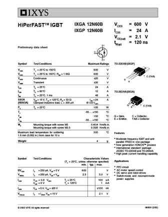
IXGA 12N60B VCES = 600 V HiPerFASTTM IGBT IXGP 12N60B IC25 = 24 A VCE(sat) = 2.1 V tfi(typ) = 120 ns Preliminary data sheet Symbol Test Conditions Maximum Ratings TO-220 AB (IXGP) VCES TJ = 25 C to 150 C 600 V VCGR TJ = 25 C to 150 C; RGE = 1 M 600 V C (TAB) VGES Continuous 20 V G E VGEM Transient 30 V IC25 TC = 25 C24 A IC90 TC = 90 C12 A TO-263 AA (IXGA) ICM TC =
ixsa12n60au1.pdf
IXSA 12N60AU1 VCES = 600 V Low VCE(sat) IGBT IC25 = 24 A with Diode VCE(sat) = 2.5 V Short Circuit SOA Capability Preliminary data sheet Symbol Test Conditions Maximum Ratings TO-263AA VCES TJ = 25 C to 150 C 600 V VCGR TJ = 25 C to 150 C; RGE = 1 M 600 V G VGES Continuous 20 V E TAB VGEM Transient 30 V G = Gate, C = Collector, IC25 TC = 25 C24 A E = Emitter
ixgh32n60as.pdf
IXGH 32N60A IXGH 32N60AS VCES = 600 V IC25 = 60 A HiPerFASTTM IGBT VCE(sat) = 2.9 V tfi = 125 ns TO-247 SMD (32N60AS) Symbol Test Conditions Maximum Ratings C (TAB) VCES TJ = 25 C to 150 C 600 V G E VCGR TJ = 25 C to 150 C; RGE = 1 M 600 V VGES Continuous 20 V TO-247 AD VGEM Transient 30 V IC25 TC = 25 C60 A IC90 TC = 90 C32 A C (TAB) G ICM TC = 25 C, 1 ms 120
2n6040g 2n6042g 2n6043g 2n6045g.pdf
PNP - 2N6040, 2N6042, NPN - 2N6043, 2N6045 Plastic Medium-Power Complementary Silicon Transistors www.onsemi.com Plastic medium-power complementary silicon transistors are designed for general-purpose amplifier and low-speed switching DARLINGTON, 8 AMPERES applications. COMPLEMENTARY SILICON Features POWER TRANSISTORS High DC Current Gain - hFE = 2500 (Typ) @ IC = 4.0 Adc 60 -
2n6040g 2n6040g 2n6045g.pdf

PNP - 2N6040, 2N6042, NPN - 2N6043, 2N6045 2N6043 and 2N6045 are Preferred Devices Plastic Medium-Power Complementary Silicon Transistors Plastic medium-power complementary silicon transistors are designed for general-purpose amplifier and low-speed switching DARLINGTON, 8 AMPERES applications. COMPLEMENTARY SILICON Features POWER TRANSISTORS High DC Current Gain - hFE = 2500 (
2n6027 2n6028.pdf
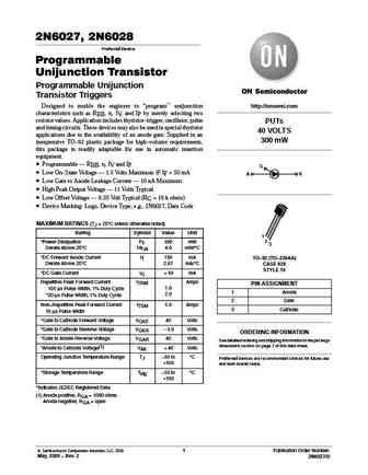
2N6027, 2N6028 Preferred Device Programmable Unijunction Transistor Programmable Unijunction Transistor Triggers Designed to enable the engineer to program unijunction http //onsemi.com characteristics such as RBB, , IV, and IP by merely selecting two resistor values. Application includes thyristor trigger, oscillator, pulse PUTs and timing circuits. These devices may als
2n6038g.pdf

2N6034G, 2N6035G, 2N6036G (PNP), 2N6038G, 2N6039G (NPN) Plastic Darlington Complementary Silicon http //onsemi.com Power Transistors 4.0 AMPERES DARLINGTON Plastic Darlington complementary silicon power transistors are designed for general purpose amplifier and low-speed switching COMPLEMENTARY SILICON applications. POWER TRANSISTORS Features 40, 60, 80 VOLTS, 40 WATTS ESD Ra
2n6034g 2n6034g 2n6038g.pdf

2N6034G, 2N6035G, 2N6036G (PNP), 2N6038G, 2N6039G (NPN) Plastic Darlington Complementary Silicon http //onsemi.com Power Transistors 4.0 AMPERES DARLINGTON Plastic Darlington complementary silicon power transistors are designed for general purpose amplifier and low-speed switching COMPLEMENTARY SILICON applications. POWER TRANSISTORS Features 40, 60, 80 VOLTS, 40 WATTS ESD Ra
fch072n60f-f085.pdf
FCH072N60F-F085 N-Channel SuperFET II FRFET MOSFET 600 V, 52 A, 72 m D Features Typical RDS(on) = 62 m at VGS = 10 V, ID = 26 A Typical Qg(tot) = 160 nC at VGS = 10V, ID = 26 A UIS Capability G Qualified to AEC Q101 G RoHS Compliant D TO-247 S S Description SuperFET II MOSFET is ON Semiconductor s brand-new high voltage super-junction (SJ) MOSFET family that is u
2n6052g.pdf
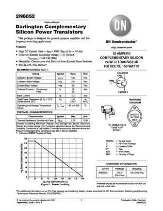
2N6052 Preferred Device Darlington Complementary Silicon Power Transistors This package is designed for general-purpose amplifier and low frequency switching applications. Features http //onsemi.com High DC Current Gain hFE = 3500 (Typ) @ IC = 5.0 Adc 12 AMPERE Collector-Emitter Sustaining Voltage @ 100 mA VCEO(sus) = 100 Vdc (Min) COMPLEMENTARY SILICON Monolit
fqp2n60c fqpf2n60c.pdf

Is Now Part of To learn more about ON Semiconductor, please visit our website at www.onsemi.com Please note As part of the Fairchild Semiconductor integration, some of the Fairchild orderable part numbers will need to change in order to meet ON Semiconductor s system requirements. Since the ON Semiconductor product management systems do not have the ability to manage part nomenclatur
2n6039g.pdf
(PNP) 2N6034, 2N6035, 2N6036; (NPN) 2N6038, 2N6039 Plastic Darlington Complementary Silicon http //onsemi.com Power Transistors Plastic Darlington complementary silicon power transistors are 4.0 AMPERES DARLINGTON designed for general purpose amplifier and low-speed switching COMPLEMENTARY SILICON applications. POWER TRANSISTORS Features 40, 60, 80 VOLTS, 40 WATTS ESD Ratings
2n6045g.pdf
PNP - 2N6040, 2N6042, NPN - 2N6043, 2N6045 2N6043 and 2N6045 are Preferred Devices Plastic Medium-Power Complementary Silicon Transistors Plastic medium-power complementary silicon transistors are designed for general-purpose amplifier and low-speed switching DARLINGTON, 8 AMPERES applications. COMPLEMENTARY SILICON Features POWER TRANSISTORS High DC Current Gain - hFE = 2500 (
fcp22n60n fcpf22n60nt.pdf

Is Now Part of To learn more about ON Semiconductor, please visit our website at www.onsemi.com Please note As part of the Fairchild Semiconductor integration, some of the Fairchild orderable part numbers will need to change in order to meet ON Semiconductor s system requirements. Since the ON Semiconductor product management systems do not have the ability to manage part nomenclatur
fqp12n60c.pdf

Is Now Part of To learn more about ON Semiconductor, please visit our website at www.onsemi.com Please note As part of the Fairchild Semiconductor integration, some of the Fairchild orderable part numbers will need to change in order to meet ON Semiconductor s system requirements. Since the ON Semiconductor product management systems do not have the ability to manage part nomenclatur
hgtg12n60a4d hgtp12n60a4d hgt1s12n60a4ds.pdf
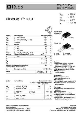
SMPS Series N-Channel IGBT with Anti-Parallel Hyperfast Diode 600 V HGTG12N60A4D, www.onsemi.com HGTP12N60A4D, HGT1S12N60A4DS C The HGTG12N60A4D, HGTP12N60A4D and HGT1S12N60A4DS are MOS gated high voltage switching devices G combining the best features of MOSFETs and bipolar transistors. These devices have the high input impedance of a MOSFET and the E low on-state conduction los
2n6036g.pdf
2N6034G, 2N6035G, 2N6036G (PNP), 2N6038G, 2N6039G (NPN) Plastic Darlington Complementary Silicon http //onsemi.com Power Transistors 4.0 AMPERES DARLINGTON Plastic Darlington complementary silicon power transistors are designed for general purpose amplifier and low-speed switching COMPLEMENTARY SILICON applications. POWER TRANSISTORS Features 40, 60, 80 VOLTS, 40 WATTS ESD Ra
hgtg12n60c3d.pdf
UFS Series N-Channel IGBT with Anti-Parallel Hyperfast Diode 24 A, 600 V HGTG12N60C3D www.onsemi.com The HGTG12N60C3D is a MOS gated high voltage switching device combining the best features of MOSFETs and bipolar C transistors. The device has the high input impedance of a MOSFET and the low on-state conduction loss of a bipolar transistor. The much lower on-state voltage drop varies
fch072n60f.pdf

Is Now Part of To learn more about ON Semiconductor, please visit our website at www.onsemi.com Please note As part of the Fairchild Semiconductor integration, some of the Fairchild orderable part numbers will need to change in order to meet ON Semiconductor s system requirements. Since the ON Semiconductor product management systems do not have the ability to manage part nomenclatur
fdp12n60nz fdpf12n60nz.pdf
November 2013 FDP12N60NZ / FDPF12N60NZ N-Channel UniFETTM II MOSFET 600 V, 12 A, 650 m Features Description RDS(on) = 530 m (Typ.) @ VGS = 10 V, ID = 6 A UniFETTM II MOSFET is Fairchild Semiconductor s high voltage MOSFET family based on advanced planar stripe and DMOS Low Gate Charge (Typ. 26 nC) technology. This advanced MOSFET family has the smallest Low Crss (Typ.
2n6042g.pdf

PNP - 2N6040, 2N6042, NPN - 2N6043, 2N6045 2N6043 and 2N6045 are Preferred Devices Plastic Medium-Power Complementary Silicon Transistors Plastic medium-power complementary silicon transistors are designed for general-purpose amplifier and low-speed switching DARLINGTON, 8 AMPERES applications. COMPLEMENTARY SILICON Features POWER TRANSISTORS High DC Current Gain - hFE = 2500 (
fqd2n60c fqu2n60c.pdf
TM QFET FQD2N60C / FQU2N60C 600V N-Channel MOSFET General Description Features These N-Channel enhancement mode power field effect 1.9A, 600V, RDS(on) = 4.7 @VGS = 10 V transistors are produced using Fairchild s proprietary, Low gate charge ( typical 8.5 nC) planar stripe, DMOS technology. Low Crss ( typical 4.3 pF) This advanced technology has been especially tailored
fqpf12n60c.pdf
November 2013 FQPF12N60C N-Channel QFET MOSFET 600 V, 12 A, 650 m Description Features These N-Channel enhancement mode power field effect 12 A, 600 V, RDS(on) = 650 m (Max.) @ VGS = 10 V, transistors are produced using Fairchild s proprietary, planar ID = 6 A stripe, DMOS technology. This advanced technology has Low Gate Charge (Typ. 48 nC) been especially tailored
hgtp12n60c3d hgt1s12n60c3ds.pdf

Is Now Part of To learn more about ON Semiconductor, please visit our website at www.onsemi.com Please note As part of the Fairchild Semiconductor integration, some of the Fairchild orderable part numbers will need to change in order to meet ON Semiconductor s system requirements. Since the ON Semiconductor product management systems do not have the ability to manage part nomenclatur
2n6043g 2n6043g 2n6042g.pdf

PNP - 2N6040, 2N6042, NPN - 2N6043, 2N6045 2N6043 and 2N6045 are Preferred Devices Plastic Medium-Power Complementary Silicon Transistors Plastic medium-power complementary silicon transistors are designed for general-purpose amplifier and low-speed switching DARLINGTON, 8 AMPERES applications. COMPLEMENTARY SILICON Features POWER TRANSISTORS High DC Current Gain - hFE = 2500 (
ndf02n60z ndp02n60z ndd02n60z.pdf
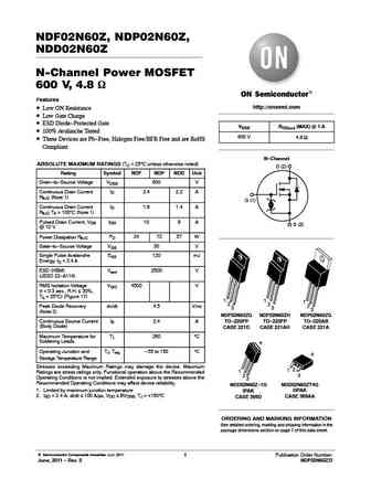
NDF02N60Z, NDP02N60Z, NDD02N60Z N-Channel Power MOSFET 600 V, 4.8 W Features http //onsemi.com Low ON Resistance Low Gate Charge ESD Diode-Protected Gate VDSS RDS(on) (MAX) @ 1 A 100% Avalanche Tested 600 V 4.8 W These Devices are Pb-Free, Halogen Free/BFR Free and are RoHS Compliant N-Channel ABSOLUTE MAXIMUM RATINGS (TC = 25 C unless otherwise noted) D (2
2n6035g 2n6035g 2n6036g.pdf

2N6034G, 2N6035G, 2N6036G (PNP), 2N6038G, 2N6039G (NPN) Plastic Darlington Complementary Silicon http //onsemi.com Power Transistors 4.0 AMPERES DARLINGTON Plastic Darlington complementary silicon power transistors are designed for general purpose amplifier and low-speed switching COMPLEMENTARY SILICON applications. POWER TRANSISTORS Features 40, 60, 80 VOLTS, 40 WATTS ESD Ra
2n60l-tm3-t 2n60g-tm3-t 2n60l-tma-t 2n60g-tma-t 2n60l-tms-t 2n60g-tms-t 2n60l-tms2-t 2n60g-tms2-t 2n60l-tms4-t 2n60g-tms4-t.pdf

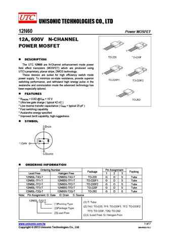
UNISONIC TECHNOLOGIES CO., LTD 2N60 Power MOSFET 2A, 600V N-CHANNEL POWER MOSFET DESCRIPTION The UTC 2N60 is a high voltage power MOSFET and is designed to have better characteristics, such as fast switching time, low gate charge, low on-state resistance and have a high rugged avalanche characteristics. This power MOSFET is usually used at high speed switching application
22n60.pdf
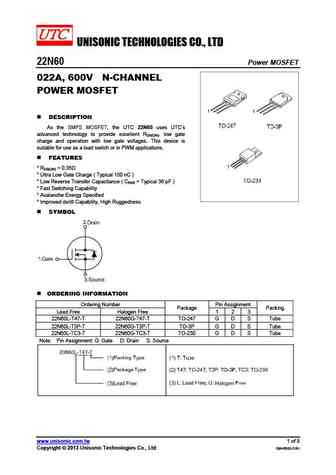
UNISONIC TECHNOLOGIES CO., LTD 22N60 Power MOSFET 022A, 600V N-CHANNEL POWER MOSFET DESCRIPTION As the SMPS MOSFET, the UTC 22N60 uses UTC s advanced technology to provide excellent RDS(ON), low gate charge and operation with low gate voltages. This device is suitable for use as a load switch or in PWM applications. FEATURES * RDS(ON) = 0.35 * Ultra Low Gate C
2n60l-ta3-t 2n60g-ta3-t 2n60l-tf1-t 2n60g-tf1-t 2n60l-tf2-t 2n60g-tf2-t 2n60l-tf3-t 2n60g-tf3-t 2n60l-tf3t-t 2n60g-tf3t-t 2n60l-tm3-t.pdf

UNISONIC TECHNOLOGIES CO., LTD 2N60 Power MOSFET 2.0A, 600V N-CHANNEL POWER MOSFET DESCRIPTION The UTC 2N60 is a high voltage power MOSFET and is designed to have better characteristics, such as fast switching time, low gate charge, low on-state resistance and have a high rugged avalanche characteristics. This power MOSFET is usually used at high speed switching applicati
2n60l-tn3-r 2n60g-tn3-r 2n60l-tnd-r 2n60g-tnd-r 2n60l-t2q-t 2n60g-t2q-t 2n60l-t60-k 2n60g-t60-k 2n60l-t6c-k 2n60g-t6c-k 2n60l-k08-5060-r.pdf

UNISONIC TECHNOLOGIES CO., LTD 2N60 Power MOSFET 2A, 600V N-CHANNEL POWER MOSFET DESCRIPTION The UTC 2N60 is a high voltage power MOSFET and is designed to have better characteristics, such as fast switching time, low gate charge, low on-state resistance and have a high rugged avalanche characteristics. This power MOSFET is usually used at high speed switching application
2n60l-ta3-t 2n60g-ta3-t 2n60l-tf1-t 2n60g-tf1-t 2n60l-tf2-t 2n60g-tf2-t 2n60l-tf3-t 2n60g-tf3-t 2n60l-tf3t-t 2n60g-tf3t-t 2n60g-k08-5060-r.pdf

UNISONIC TECHNOLOGIES CO., LTD 2N60 Power MOSFET 2A, 600V N-CHANNEL POWER MOSFET DESCRIPTION The UTC 2N60 is a high voltage power MOSFET and is designed to have better characteristics, such as fast switching time, low gate charge, low on-state resistance and have a high rugged avalanche characteristics. This power MOSFET is usually used at high speed switching application
12n60l-ta3-t 12n60g-ta3-t 12n60l-tf1-t 12n60g-tf1-t 12n60l-tf2-t 12n60g-tf2-t 12n60l-tf3-t 12n60g-tf3-t 12n60l-t2q-t 12n60g-t2q-t 12n60l-t3p-t 12n60g-t3p-t.pdf
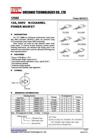
UNISONIC TECHNOLOGIES CO., LTD 12N60 Power MOSFET 12A, 600V N-CHANNEL POWER MOSFET DESCRIPTION The UTC 12N60 are N-Channel enhancement mode power field effect transistors (MOSFET) which are produced using UTC s proprietary, planar stripe, DMOS technology. These devices are suited for high efficiency switch mode power supply. To minimize on-state resistance, provide supe
2n60l-t2q-t 2n60g-t2q-t 2n60l-t60-k 2n60g-t60-k 2n60l-t6c-k 2n60g-t6c-k 2n60g-e-k08-5060-r 2n60g-tm3-t 2n60g-tnd-r.pdf
UNISONIC TECHNOLOGIES CO., LTD 2N60 Power MOSFET 2.0A, 600V N-CHANNEL POWER MOSFET DESCRIPTION The UTC 2N60 is a high voltage power MOSFET and is designed to have better characteristics, such as fast switching time, low gate charge, low on-state resistance and have a high rugged avalanche characteristics. This power MOSFET is usually used at high speed switching applicati
2n60l-t60-t 2n60g-t60-t 2n60l-aa3-r 2n60g-aa3-r 2n60l-ta3-t 2n60g-ta3-t 2n60l-tf3-t 2n60g-tf3-t 2n60l-tf1-t 2n60g-tf1-t.pdf

UNISONIC TECHNOLOGIES CO., LTD 2N60-CB Power MOSFET 2A, 600V N-CHANNEL POWER MOSFET DESCRIPTION The UTC 2N60-CB is a high voltage power MOSFET and is designed to have better characteristics, such as fast switching time, low gate charge, low on-state resistance and have a high rugged avalanche characteristics. This power MOSFET is usually used at high speed switching appli
12n60.pdf
UNISONIC TECHNOLOGIES CO., LTD 12N60 Power MOSFET 12A, 600V N-CHANNEL POWER MOSFET DESCRIPTION The UTC 12N60 are N-Channel enhancement mode power field effect transistors (MOSFET) which are produced using UTC s proprietary, planar stripe, DMOS technology. These devices are suited for high efficiency switch mode power supply. To minimize on-state resistance, provide superi
2n60l-tf2-t 2n60g-tf2-t 2n60l-tf3t-t 2n60g-tf3t-t 2n60l-tm3-t 2n60g-tm3-t 2n60l-tms-t 2n60g-tms-t 2n60l-tms2-t 2n60g-tms2-t.pdf

UNISONIC TECHNOLOGIES CO., LTD 2N60-CB Power MOSFET 2A, 600V N-CHANNEL POWER MOSFET DESCRIPTION The UTC 2N60-CB is a high voltage power MOSFET and is designed to have better characteristics, such as fast switching time, low gate charge, low on-state resistance and have a high rugged avalanche characteristics. This power MOSFET is usually used at high speed switching appli
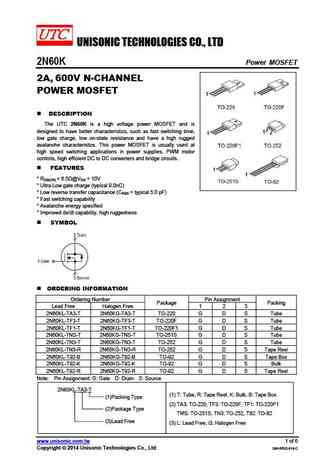
2n60k.pdf
UNISONIC TECHNOLOGIES CO., LTD 2N60K Power MOSFET 2A, 600V N-CHANNEL POWER MOSFET DESCRIPTION The UTC 2N60K is a high voltage power MOSFET and is designed to have better characteristics, such as fast switching time, low gate charge, low on-state resistance and have a high rugged avalanche characteristics. This power MOSFET is usually used at high speed switching applicatio
2n60l-tma-t 2n60g-tma-t 2n60l-tms-t 2n60g-tms-t 2n60l-tms2-t 2n60g-tms2-t 2n60l-tms4-t 2n60g-tms4-t 2n60l-tn3-r 2n60g-tn3-r 2n60l-tnd-r.pdf

UNISONIC TECHNOLOGIES CO., LTD 2N60 Power MOSFET 2.0A, 600V N-CHANNEL POWER MOSFET DESCRIPTION The UTC 2N60 is a high voltage power MOSFET and is designed to have better characteristics, such as fast switching time, low gate charge, low on-state resistance and have a high rugged avalanche characteristics. This power MOSFET is usually used at high speed switching applicati
2n60l.pdf
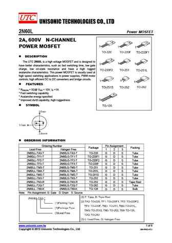
UNISONIC TECHNOLOGIES CO., LTD 2N60L Power MOSFET 2A, 600V N-CHANNEL POWER MOSFET DESCRIPTION The UTC 2N60L is a high voltage MOSFET and is designed to have better characteristics, such as fast switching time, low gate charge, low on-state resistance and have a high rugged avalanche characteristics. This power MOSFET is usually used at high speed switching applications in
2n60l-tms4-t 2n60g-tms4-t 2n60l-tn3-r 2n60g-tn3-r 2n60l-tnd-r 2n60g-tnd-r 2n60l-k08-5060-r 2n60g-k08-5060-r.pdf
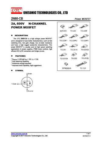
UNISONIC TECHNOLOGIES CO., LTD 2N60-CB Power MOSFET 2A, 600V N-CHANNEL POWER MOSFET DESCRIPTION The UTC 2N60-CB is a high voltage power MOSFET and is designed to have better characteristics, such as fast switching time, low gate charge, low on-state resistance and have a high rugged avalanche characteristics. This power MOSFET is usually used at high speed switching appli
2n6055-2n6053.pdf
2N6053 PNP 2N6055 NPN COMPLEMENTARY POWER DARLINGTON The 2N6053 is a silicon epitaxial base PNP transistor in monolithic Darlington configuration and are mounted in Jedec TO-3 metal case. They are intended for use in power linear and switching applications. The complementary NPN type is the 2N6055 ABSOLUTE MAXIMUM RATINGS Symbol Ratings Value Unit 2N6053 VCEO #Collector-Emitter Volta
2n6050-2n6051-2n6052-2n6057-2n6058-2n6059.pdf
POWER COMPLEMENTARY POWER COMPLEMENTARY SILICON TRANSISTORS SILICON TRANSISTORS The 2N6050, 2N6051 and 2N6052 are silicon epitaxial-base PNP transistors in monolithic Darlington configuration mounted in Jedec TO-3 metal case. They are inteded for use in power linear and low frequency switching applications. The complementary NPN types are 2N6057, 2N6058 and 2N6059 respectively.
fmi12n60es.pdf
FMI12N60ES FUJI POWER MOSFET Super FAP-E3S series N-CHANNEL SILICON POWER MOSFET Features Outline Drawings [mm] Equivalent circuit schematic Maintains both low power loss and low noise T-Pack(L) Lower R (on) characteristic DS More controllable switching dv/dt by gate resistance Drain(D) Smaller V ringing waveform during switching GS Narrow band of the gate threshold voltage (4.2 0.5
fml12n60es.pdf
http //www.fujisemi.com FML12N60ES FUJI POWER MOSFET Super FAP-E3 series N-CHANNEL SILICON POWER MOSFET Features Outline Drawings [mm] Equivalent circuit schematic Maintains both low power loss and low noise TFP 9.0 0.2 7.0 0.2 0.4 0.1 Lower R (on) characteristic DS 4 More controllable switching dv/dt by gate resistance 4 D Smaller V ringing waveform during switching GS Narrow
fmv12n60es.pdf
FMV12N60ES FUJI POWER MOSFET Super FAP-E3S series N-CHANNEL SILICON POWER MOSFET Features Outline Drawings [mm] Equivalent circuit schematic Maintains both low power loss and low noise TO-220F(SLS) Lower R (on) characteristic DS More controllable switching dv/dt by gate resistance Drain(D) Smaller V ringing waveform during switching GS Narrow band of the gate threshold voltage (4.2
fmc12n60es.pdf

FMC12N60ES FUJI POWER MOSFET Super FAP-E3S series N-CHANNEL SILICON POWER MOSFET Features Outline Drawings [mm] Equivalent circuit schematic Maintains both low power loss and low noise T-Pack(S) Lower R (on) characteristic DS More controllable switching dv/dt by gate resistance Drain(D) Smaller V ringing waveform during switching GS Narrow band of the gate threshold voltage (4.2 0.5
fmp12n60es.pdf
FMP12N60ES FUJI POWER MOSFET Super FAP-E3S series N-CHANNEL SILICON POWER MOSFET Features Outline Drawings [mm] Equivalent circuit schematic Maintains both low power loss and low noise TO-220AB Lower R (on) characteristic DS More controllable switching dv/dt by gate resistance Drain(D) Smaller V ringing waveform during switching GS Narrow band of the gate threshold voltage (4.2 0.5V
hgtp12n60c3.pdf
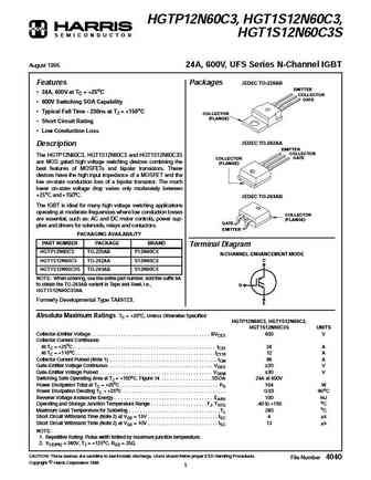
HGTP12N60C3, HGT1S12N60C3, S E M I C O N D U C T O R HGT1S12N60C3S August 1995 24A, 600V, UFS Series N-Channel IGBT Features Packages JEDEC TO-220AB EMITTER 24A, 600V at TC = +25oC COLLECTOR GATE 600V Switching SOA Capability Typical Fall Time - 230ns at TJ = +150oC COLLECTOR (FLANGE) Short Circuit Rating Low Conduction Loss JEDEC TO-262AA Description EMITTER
hgtg12n60d1d.pdf
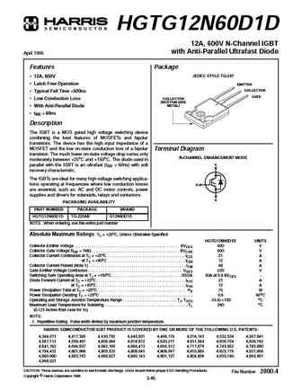
S E M I C O N D U C T O R HGTG12N60D1D 12A, 600V N-Channel IGBT with Anti-Parallel Ultrafast Diode April 1995 Features Package JEDEC STYLE TO-247 12A, 600V Latch Free Operation EMITTER COLLECTOR Typical Fall Time
hgtg12n60c3d .pdf
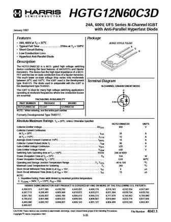
S E M I C O N D U C T O R HGTG12N60C3D 24A, 600V, UFS Series N-Channel IGBT with Anti-Parallel Hyperfast Diode January 1997 Features Package 24A, 600V at TC = 25oC JEDEC STYLE TO-247 Typical Fall Time . . . . . . . . . . . . . . 210ns at TJ = 150oC E C Short Circuit Rating G Low Conduction Loss Hyperfast Anti-Parallel Diode Description The HGTG12N60C3D is a MO
hgtg12n60c3d.pdf
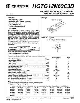
S E M I C O N D U C T O R HGTG12N60C3D 24A, 600V, UFS Series N-Channel IGBT with Anti-Parallel Hyperfast Diode August 1995 Features Package 24A, 600V at TC = +25oC JEDEC STYLE TO-247 Typical Fall Time - 210ns at TJ = +150oC E C Short Circuit Rating G Low Conduction Loss Hyperfast Anti-Parallel Diode Description The HGTG12N60C3D is a MOS gated high voltage swit
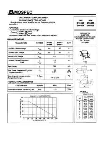
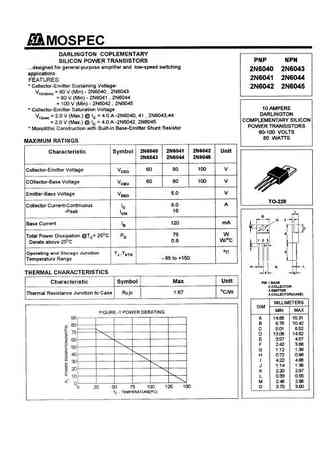
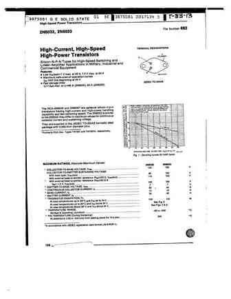
cs2n60-f.pdf
CS2N60(F) CS2N60(F) VDMOS 1. CS2N60(F) N 600V VDMOS VDSS RDS(ON)MAX ID CS2N60 TO-220
2n6077.pdf
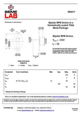
2N6077 Dimensions in mm (inches). Bipolar NPN Device in a Hermetically sealed TO66 6.35 (0.250) Metal Package. 8.64 (0.340) 3.68 (0.145) rad. 3.61 (0.142) max. 4.08(0.161) rad. Bipolar NPN Device. 1 2 VCEO = 275V IC = 7A All Semelab hermetically sealed products can be processed in accordance with the requirements of BS, CECC and JAN, JANTX, JANTXV and JANS speci
2n6079.pdf
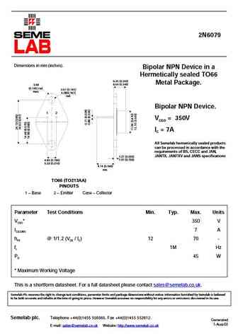
2N6079 Dimensions in mm (inches). Bipolar NPN Device in a Hermetically sealed TO66 6.35 (0.250) Metal Package. 8.64 (0.340) 3.68 (0.145) rad. 3.61 (0.142) max. 4.08(0.161) rad. Bipolar NPN Device. 1 2 VCEO = 350V IC = 7A All Semelab hermetically sealed products can be processed in accordance with the requirements of BS, CECC and JAN, JANTX, JANTXV and JANS speci
2n6078.pdf
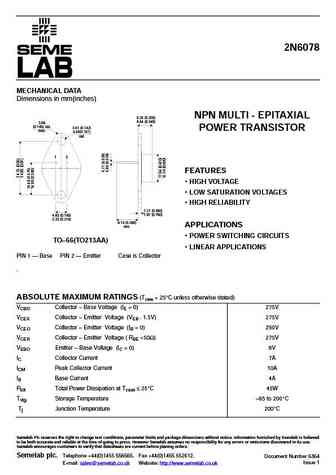
2N6078 MECHANICAL DATA Dimensions in mm(inches) NPN MULTI - EPITAXIAL 6.35 (0.250) 8.64 (0.340) 3.68 (0.145) rad. 3.61 (0.142) POWER TRANSISTOR max. 4.08(0.161) rad. 1 2 FEATURES HIGH VOLTAGE LOW SATURATION VOLTAGES HIGH RELIABILITY 1.27 (0.050) 4.83 (0.190) 1.91 (0.750) 5.33 (0.210) 9.14 (0.360) APPLICATIONS min. POWER SWITCHING CIRCUITS TO 66(TO213AA
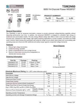
tsm2n60ch tsm2n60cp tsm2n60cz.pdf
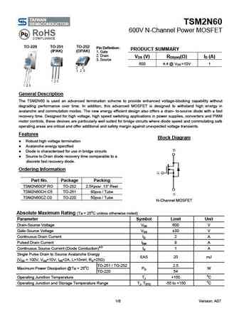
TSM2N60 600V N-Channel Power MOSFET TO-220 TO-251 TO-252 Pin Definition PRODUCT SUMMARY (IPAK) (DPAK) 1. Gate 2. Drain VDS (V) RDS(on)( ) ID (A) 3. Source 600 4.4 @ VGS =10V 1 General Description The TSM2N60 is used an advanced termination scheme to provide enhanced voltage-blocking capability without degrading performance over time. In addition, this advanced MOSFE
tsm2n60scw.pdf
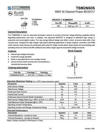
TSM2N60S 600V N-Channel Power MOSFET SOT-223 Pin Definition PRODUCT SUMMARY 1. Gate 2. Drain VDS (V) RDS(on)( ) ID (A) 3. Source 600 5 @ VGS =10V 0.6 General Description The TSM2N60S is used an advanced termination scheme to provide enhanced voltage-blocking capability without degrading performance over time. In addition, this advanced MOSFET is designed to withstand
2n6093.pdf
2N6093 NPN SILICON RF POWER TRANSISTOR PACKAGE STYLE TO-217 DESCRIPTION The 2N6093 is a High Gain Linear RF Power Amplifier Used in Class A or Class B Applications With Individual Ballast Emitter Resistor and Built in Temperature Sensing Diode. MAXIMUM RATINGS IC 10 A VCE 35 V PDISS 83.3 W @ TC = 75 OC 1 = Emitter & Diode Cathode TJ -65 OC to +200 OC 2 = Collector 3 = Base TS
2n6050 2n6051 2n6052 2n6057 2n6058 2n6059.pdf
A Boca Semiconductor Corp. BSC A Boca Semiconductor Corp. BSC http //www.bocasemi.com A Boca Semiconductor Corp. BSC http //www.bocasemi.com A Boca Semiconductor Corp. BSC http //www.bocasemi.com
2n6034-39.pdf
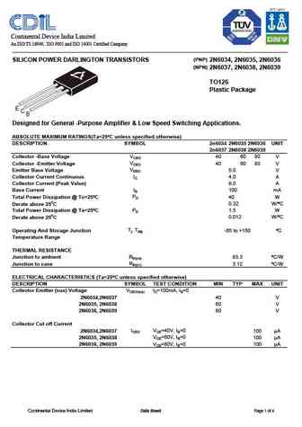
Continental Device India Limited An ISO/TS 16949, ISO 9001 and ISO 14001 Certified Company (PNP) SILICON POWER DARLINGTON TRANSISTORS 2N6034, 2N6035, 2N6036 (NPN) 2N6037, 2N6038, 2N6039 TO126 Plastic Package E C B Designed for General -Purpose Amplifier & Low Speed Switching Applications. ABSOLUTE MAXIMUM RATINGS(Ta=25 C unless specified otherwise) DESCRIPTION SYMBOL 2n6034 2N6
cjpf02n60.pdf
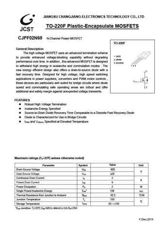
JIANGSU CHANGJIANG ELECTRONICS TECHNOLOGY CO., LTD TO-220F Plastic-Encapsulate MOSFETS CJPF02N60 N-Channel Power MOSFET TO-220F General Description The high voltage MOSFET uses an advanced termination scheme 1. GATE to provide enhanced voltage-blocking capability without degrading 2. DRAIN performance over time. In addition , this advanced MOSFET is designed 3. SOURCE
cjp02n60.pdf

JIANGSU CHANGJIANG ELECTRONICS TECHNOLOGY CO., LTD TO-220-3L Plastic-Encapsulate MOSFETS CJP02N60 N-Channel Power MOSFET TO-220-3L General Description The high voltage MOSFET uses an advanced termination scheme to provide enhanced voltage-blocking capability without degrading performance over time. In addition , this advanced MOSFET is designed to withstand high energy in ava
cji02n60.pdf
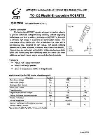
JIANGSU CHANGJIANG ELECTRONICS TECHNOLOGY CO., LTD TO-126 Plastic-Encapsulate MOSFETS CJI02N60 N-Channel Power MOSFET TO-126 General Description The high voltage MOSFET uses an advanced termination scheme to provide enhanced voltage-blocking capability without degrading performance over time. In addition , this advanced MOSFET is designed to withstand high energy in avalanche
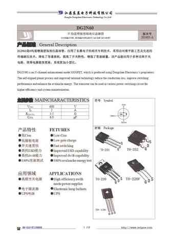
cju02n60.pdf
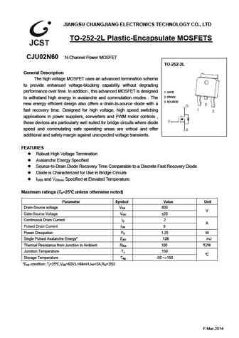
JIANGSU CHANGJIANG ELECTRONICS TECHNOLOGY CO., LTD TO-252-2L Plastic-Encapsulate MOSFETS CJU02N60 N-Channel Power MOSFET TO-252-2L General Description The high voltage MOSFET uses an advanced termination scheme to provide enhanced voltage-blocking capability without degrading performance over time. In addition , this advanced MOSFET is designed 1. GATE 2. DRAIN to withsta
cjp12n60.pdf
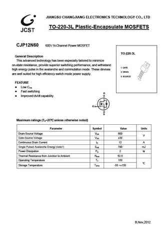
JIANGSU CHANGJIANG ELECTRONICS TECHNOLOGY CO., LTD TO-220-3L Plastic-Encapsulate MOSFETS CJP12N60 600V N-Channel Power MOSFET TO-220-3L General Description This advanced technology has been especially tailored to minimize on-state resistance, provide superior switching performance, and withistand 1. GATE high energy pulse in the avalanche and commutation mode. These devices
cjd02n60.pdf
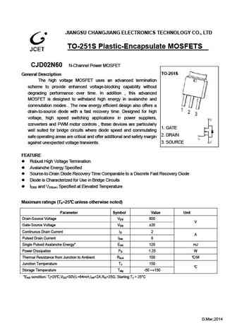
JIANGSU CHANGJIANG ELECTRONICS TECHNOLOGY CO., LTD TO-251S Plastic-Encapsulate MOSFETS CJD02N60 N-Channel Power MOSFET TO-251S General Description The high voltage MOSFET uses an advanced termination scheme to provide enhanced voltage-blocking capability without degrading performance over time. In addition , this advanced MOSFET is designed to withstand high energy in avalanch
cjpf12n60.pdf
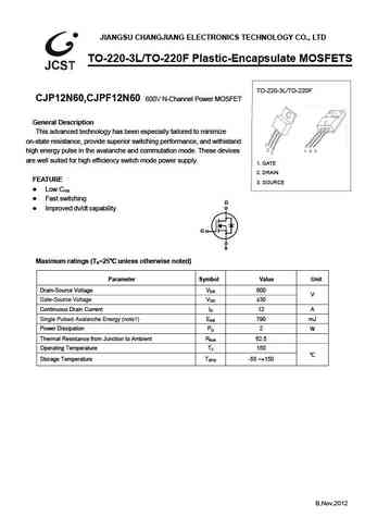
JIANGSU CHANGJIANG ELECTRONICS TECHNOLOGY CO., LTD TO-220 / F Plastic-Encapsulate MOSFETS CJP12N60,CJPF12N60 600V N-Channel Power MOSFET General Description This advanced technology has been especially tailored to minimize on-state resistance, provide superior switching performance, and withistand high energy pulse in the avalanche and commutation mode. T
2n6029 2n6030.pdf
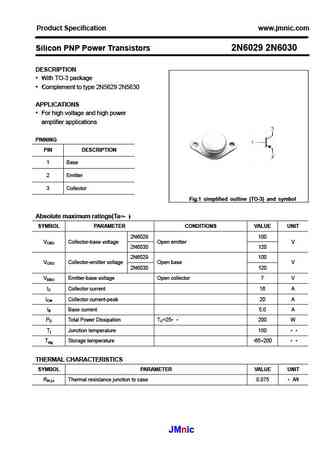
Product Specification www.jmnic.com Silicon PNP Power Transistors 2N6029 2N6030 DESCRIPTION With TO-3 package Complement to type 2N5629 2N5630 APPLICATIONS For high voltage and high power amplifier applications PINNING PIN DESCRIPTION 1 Base 2 Emitter 3 Collector Fig.1 simplified outline (TO-3) and symbol Absolute maximum ratings(Ta= ) SYMBOL PARAMETER CONDITI
2n6098 2n6099 2n6100 2n6101.pdf
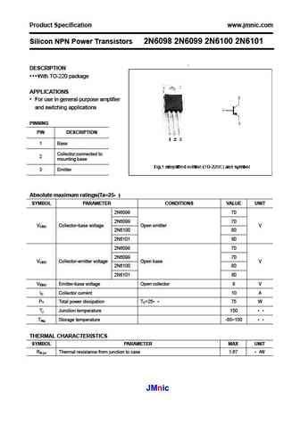
Product Specification www.jmnic.com Silicon NPN Power Transistors 2N6098 2N6099 2N6100 2N6101 DESCRIPTION With TO-220 package APPLICATIONS For use in general-purpose amplifier and switching applications PINNING PIN DESCRIPTION 1 Base Collector;connected to 2 mounting base 3 Emitter Absolute maximum ratings(Ta=25 ) SYMBOL PARAMETER CONDITIONS VALUE UNIT 2N
2n6058 2n6059.pdf
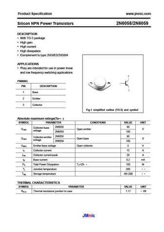
Product Specification www.jmnic.com Silicon NPN Power Transistors 2N6058/2N6059 DESCRIPTION With TO-3 package High gain High current High dissipation Complement to type 2N5883/2N5884 APPLICATIONS They are intended for use in power linear and low frequency switching applications PINNING PIN DESCRIPTION 1 Base 2 Emitter 3 Collector Fig.1 simplified outline
2n6077 2n6078 2n6079.pdf
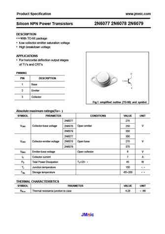
Product Specification www.jmnic.com Silicon NPN Power Transistors 2N6077 2N6078 2N6079 DESCRIPTION With TO-66 package Low collector-emitter saturation voltage High breakdown voltage APPLICATIONS For horizontal deflection output stages of TV s and CRT s PINNING PIN DESCRIPTION 1 Base 2 Emitter 3 Collector Fig.1 simplified outline (TO-66) and symbol Abso
kf12n60p-f.pdf
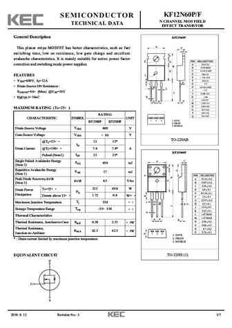
KF12N60P/F SEMICONDUCTOR N CHANNEL MOS FIELD TECHNICAL DATA EFFECT TRANSISTOR General Description KF12N60P This planar stripe MOSFET has better characteristics, such as fast switching time, low on resistance, low gate charge and excellent avalanche characteristics. It is mainly suitable for active power factor correction and switching mode power supplies. FEATURES VDSS=600V, ID=
kmb8d2n60qa.pdf
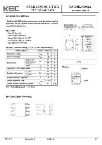
SEMICONDUCTOR KMB8D2N60QA TECHNICAL DATA N-Ch Trench MOSFET GENERAL DESCRIPTION This Trench MOSFET has better characteristics, such as fast switching time, low on resistance, low gate charge and excellent avalanche characteristiscs. It is mainly suitable for Back-light Inverter. H T D P G L FEATURES VDSS=60V, ID=8.2A. A Drain-Source ON Resistance. DIM MILLIMETERS A _ + RDS(ON)=
kf2n60p-f.pdf
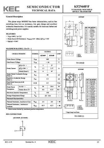
KF2N60P/F SEMICONDUCTOR N CHANNEL MOS FIELD TECHNICAL DATA EFFECT TRANSISTOR General Description KF2N60P A This planar stripe MOSFET has better characteristics, such as fast O C switching time, low on resistance, low gate charge and excellent F avalanche characteristics. It is mainly suitable for electronic ballast and E DIM MILLIMETERS G _ switching mode power supplies. A 9.9
kf12n60p kf12n60f.pdf
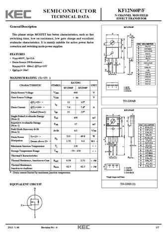
KF12N60P/F SEMICONDUCTOR N CHANNEL MOS FIELD TECHNICAL DATA EFFECT TRANSISTOR General Description KF12N60P A This planar stripe MOSFET has better characteristics, such as fast O C switching time, low on resistance, low gate charge and excellent F avalanche characteristics. It is mainly suitable for active power factor E DIM MILLIMETERS G _ + correction and switching mode power
kf2n60l.pdf
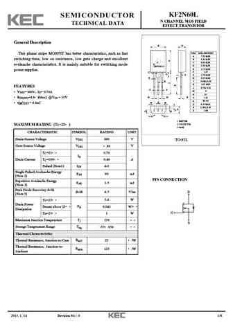
KF2N60L SEMICONDUCTOR N CHANNEL MOS FIELD TECHNICAL DATA EFFECT TRANSISTOR General Description B D DIM MILLIMETERS This planar stripe MOSFET has better characteristics, such as fast A 7.20 MAX switching time, low on resistance, low gate charge and excellent B 5.20 MAX C 0.60 MAX avalanche characteristics. It is mainly suitable for switching mode P D 2.50 MAX DEPTH 0.2 E 1.15 MAX
kf2n60d-i.pdf
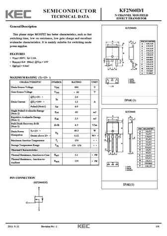
KF2N60D/I SEMICONDUCTOR N CHANNEL MOS FIELD TECHNICAL DATA EFFECT TRANSISTOR General Description KF2N60D This planar stripe MOSFET has better characteristics, such as fast switching time, low on resistance, low gate charge and excellent A K DIM MILLIMETERS avalanche characteristics. It is mainly suitable for switching mode L C D _ A 6.60 + 0.20 _ B 6.10 + 0.20 power supplies.
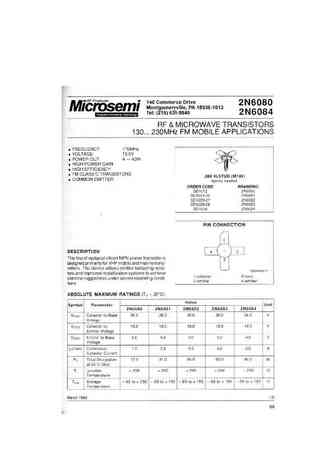
2n60p 2n60f 2n60i 2n60d.pdf

2N60 Surface Mount N-Channel Power MOSFET DRAIN CURRENT P b Lead(Pb)-Free 2 AMPERES DRAIN SOURCE VOLTAGE Description 600 VOLTAGE This advanced technology has been especially tailored to minimize on-state resistance, provide superior switching performance, and withstand high energy pulse in the avalanche and commutation mode. These devices are well suited for high efficiency switche
h12n60.pdf
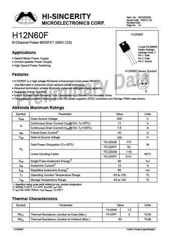
Spec. No. MOS200902 HI-SINCERITY Issued Date 2009.01.20 Revised Date MICROELECTRONICS CORP. Page No. 1/4 H12N60F H12N60F N-Channel Power MOSFET (600V,12A) 3-Lead TO-220FP) Plastic Package Package Code F Applications Pin 1 Gate Switch Mode Power Supply Pin 2 Drain Pin 3 Source Uninterruptable Power Supply 3 2 1 High Speed Power Switch
h02n60.pdf
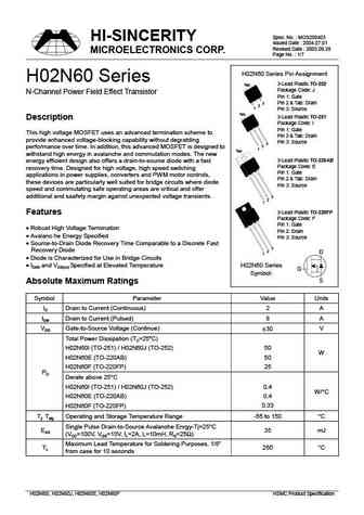
Spec. No. MOS200403 HI-SINCERITY Issued Date 2004.07.01 Revised Date 2005.09.28 MICROELECTRONICS CORP. Page No. 1/7 H02N60 Series Pin Assignment H02N60 Series Tab 3-Lead Plastic TO-252 Package Code J N-Channel Power Field Effect Transistor Pin 1 Gate 3 Pin 2 & Tab Drain 2 1 Pin 3 Source Tab 3-Lead Plastic TO-251 Description Package Code I Pin 1 Gate This high
h02n60s.pdf
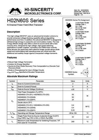
Spec. No. MOS200504 HI-SINCERITY Issued Date 2005.05.01 Revised Date 2005.09.28 MICROELECTRONICS CORP. Page No. 1/6 H02N60S Series Pin Assignment H02N60S Series Tab 3-Lead Plastic TO-252 Package Code J N-Channel Power Field Effect Transistor Pin 1 Gate 3 Pin 2 & Tab Drain 2 1 Pin 3 Source Tab 3-Lead Plastic TO-251 Description Package Code I Pin 1 Gate This hig
aow12n60 aowf12n60.pdf
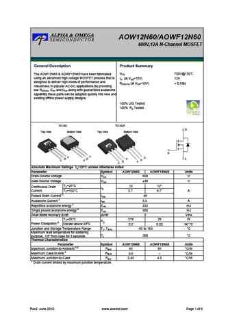
AOW12N60/AOWF12N60 600V,12A N-Channel MOSFET General Description Product Summary VDS 700V@150 The AOW12N60 & AOWF12N60 have been fabricated using an advanced high voltage MOSFET process that is ID (at VGS=10V) 12A designed to deliver high levels of performance and RDS(ON) (at VGS=10V)
aou2n60a.pdf

AOD2N60A/AOI2N60A/AOU2N60A 600V,2A N-Channel MOSFET General Description Product Summary VDS @ Tj,max 700V Advanced High Voltage MOSFET technology Low RDS(ON) ID (at VGS=10V) 2A Low Ciss and Crss RDS(ON) (at VGS=10V)
aod2n60a aoi2n60a aou2n60a.pdf
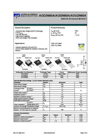
AOD2N60A/AOI2N60A/AOU2N60A 600V,2A N-Channel MOSFET General Description Product Summary VDS @ Tj,max 700V Advanced High Voltage MOSFET technology Low RDS(ON) ID (at VGS=10V) 2A Low Ciss and Crss RDS(ON) (at VGS=10V)
aowf12n60.pdf
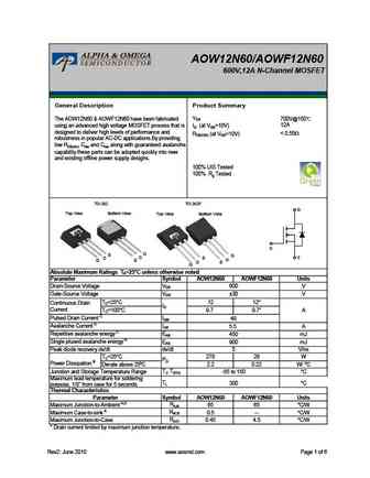
AOW12N60/AOWF12N60 600V,12A N-Channel MOSFET General Description Product Summary VDS The AOW12N60 & AOWF12N60 have been fabricated 700V@150 12A using an advanced high voltage MOSFET process that is ID (at VGS=10V) designed to deliver high levels of performance and
aoi2n60.pdf
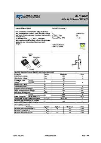
AOI2N60 600V, 2A N-Channel MOSFET General Description Product Summary The AOI2N60 has been fabricated using an advanced high voltage MOSFET process that is designed to deliver VDS 700V@150 high levels of performance and robustness in popular AC- ID (at VGS=10V) 2A DC applications. RDS(ON) (at VGS=10V)
aot12n60.pdf

AOT12N60/AOTF12N60 600V,12A N-Channel MOSFET General Description Product Summary VDS 700V@150 The AOT12N60 & AOTF12N60 have been fabricated using an advanced high voltage MOSFET process that is ID (at VGS=10V) 12A designed to deliver high levels of performance and RDS(ON) (at VGS=10V)
aotf2n60.pdf

AOT2N60/AOTF2N60 600V,2A N-Channel MOSFET General Description Product Summary VDS 700V@150 The AOT2N60 & AOTF2N60 have been fabricated using an advanced high voltage MOSFET process that is ID (at VGS=10V) 2A designed to deliver high levels of performance and RDS(ON) (at VGS=10V)
aod2n60.pdf
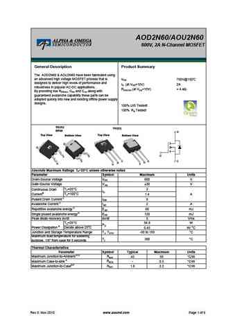
AOD2N60/AOU2N60 600V, 2A N-Channel MOSFET General Description Product Summary The AOD2N60 & AOU2N60 have been fabricated using an advanced high voltage MOSFET process that is VDS 700V@150 designed to deliver high levels of performance and ID (at VGS=10V) 2A robustness in popular AC-DC applications. RDS(ON) (at VGS=10V)
aotf12n60.pdf

AOT12N60/AOTF12N60 600V,12A N-Channel MOSFET General Description Product Summary VDS 700V@150 The AOT12N60 & AOTF12N60 have been fabricated using an advanced high voltage MOSFET process that is ID (at VGS=10V) 12A designed to deliver high levels of performance and RDS(ON) (at VGS=10V)
aou2n60.pdf

AOD2N60/AOU2N60 600V, 2A N-Channel MOSFET General Description Product Summary The AOD2N60 & AOU2N60 have been fabricated using an advanced high voltage MOSFET process that is VDS 700V@150 designed to deliver high levels of performance and ID (at VGS=10V) 2A robustness in popular AC-DC applications. RDS(ON) (at VGS=10V)
aot12n60fd.pdf

AOT12N60FD/AOB12N60FD/AOTF12N60FD 600V, 12A N-Channel MOSFET General Description Product Summary VDS 700V@150 The AOT12N60FD/AOB12N60FD/AOTF12N60FD have been fabricated using an advanced high voltage MOSFET ID (at VGS=10V) 12A process that is designed to deliver high levels of RDS(ON) (at VGS=10V)
aotf12n60fd.pdf
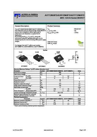
AOT12N60FD/AOB12N60FD/AOTF12N60FD 600V, 12A N-Channel MOSFET General Description Product Summary VDS 700V@150 The AOT12N60FD/AOB12N60FD/AOTF12N60FD have been fabricated using an advanced high voltage MOSFET ID (at VGS=10V) 12A process that is designed to deliver high levels of RDS(ON) (at VGS=10V)
aob12n60fd.pdf

AOT12N60FD/AOB12N60FD/AOTF12N60FD 600V, 12A N-Channel MOSFET General Description Product Summary VDS 700V@150 The AOT12N60FD/AOB12N60FD/AOTF12N60FD have been fabricated using an advanced high voltage MOSFET ID (at VGS=10V) 12A process that is designed to deliver high levels of RDS(ON) (at VGS=10V)
aot2n60.pdf
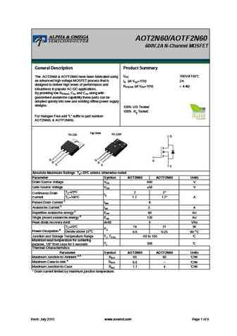
AOT2N60/AOTF2N60 600V,2A N-Channel MOSFET General Description Product Summary VDS 700V@150 The AOT2N60 & AOTF2N60 have been fabricated using an advanced high voltage MOSFET process that is ID (at VGS=10V) 2A designed to deliver high levels of performance and RDS(ON) (at VGS=10V)
aot12n60 aotf12n60.pdf
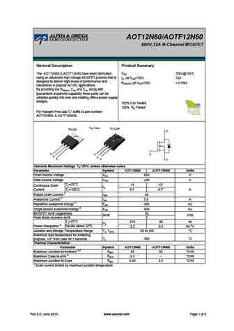
AOT12N60/AOTF12N60 600V,12A N-Channel MOSFET General Description Product Summary VDS 700V@150 The AOT12N60 & AOTF12N60 have been fabricated using an advanced high voltage MOSFET process that is ID (at VGS=10V) 12A designed to deliver high levels of performance and RDS(ON) (at VGS=10V)
aod2n60 aou2n60.pdf
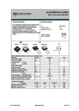
AOD2N60/AOU2N60 600V, 2A N-Channel MOSFET General Description Product Summary The AOD2N60 & AOU2N60 have been fabricated using an advanced high voltage MOSFET process that is VDS 700V@150 designed to deliver high levels of performance and ID (at VGS=10V) 2A robustness in popular AC-DC applications. RDS(ON) (at VGS=10V)
aow12n60.pdf

AOW12N60/AOWF12N60 600V,12A N-Channel MOSFET General Description Product Summary VDS The AOW12N60 & AOWF12N60 have been fabricated 700V@150 12A using an advanced high voltage MOSFET process that is ID (at VGS=10V) designed to deliver high levels of performance and
aoy2n60.pdf
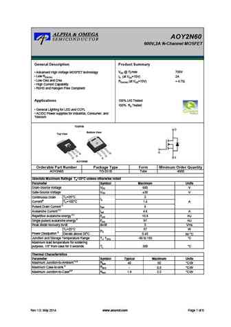
AOY2N60 600V,2A N-Channel MOSFET General Description Product Summary VDS @ Tj,max 700V Advanced High Voltage MOSFET technology Low RDS(ON) ID (at VGS=10V) 2A Low Ciss and Crss RDS(ON) (at VGS=10V)
aoi2n60a.pdf

AOD2N60A/AOI2N60A/AOU2N60A 600V,2A N-Channel MOSFET General Description Product Summary VDS @ Tj,max 700V Advanced High Voltage MOSFET technology Low RDS(ON) ID (at VGS=10V) 2A Low Ciss and Crss RDS(ON) (at VGS=10V)
aod2n60a.pdf

AOD2N60A/AOI2N60A/AOU2N60A 600V,2A N-Channel MOSFET General Description Product Summary VDS @ Tj,max 700V Advanced High Voltage MOSFET technology Low RDS(ON) ID (at VGS=10V) 2A Low Ciss and Crss RDS(ON) (at VGS=10V)
ap02n60p-a-hf.pdf
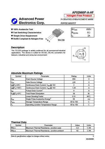
AP02N60P-A-HF Halogen-Free Product Advanced Power N-CHANNEL ENHANCEMENT MODE Electronics Corp. POWER MOSFET 100% Avalanche Test BVDSS 650V Fast Switching Characteristics RDS(ON) 8 Simple Drive Requirement ID 2A RoHS Compliant & Halogen-Free G D TO-220 S Description D The TO-220 package is widely preferred for all commercial-industrial applications. The device is
ap02n60h ap02n60j.pdf

AP02N60H/J RoHS-compliant Product Advanced Power N-CHANNEL ENHANCEMENT MODE Electronics Corp. POWER MOSFET Low Gate Charge BVDSS 600V D 100% Avalanche Test RDS(ON) 8 Simple Drive Requirement ID 1.6A G S Description G D TO-252(H) S The TO-252 package is widely preferred for all commercial-industrial surface mount applications and suited for AC/DC converters. The th
ap02n60i.pdf
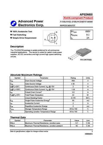
AP02N60I RoHS-compliant Product Advanced Power N-CHANNEL ENHANCEMENT MODE Electronics Corp. POWER MOSFET 100% Avalanche Test BVDSS 600V D Fast Switching RDS(ON) 8 Simple Drive Requirement ID 2A G S Description The TO-220CFM package is widely preferred for all commercial- industrial applications. The device is suited for switch mode power supplies ,AC-DC converters and
ap02n60p.pdf
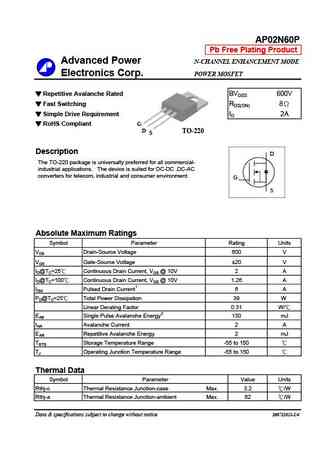
AP02N60P Pb Free Plating Product Advanced Power N-CHANNEL ENHANCEMENT MODE Electronics Corp. POWER MOSFET Repetitive Avalanche Rated BVDSS 600V Fast Switching RDS(ON) 8 Simple Drive Requirement ID 2A RoHS Compliant G D TO-220 S Description D The TO-220 package is universally preferred for all commerci
ap02n60p-hf.pdf
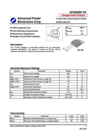
AP02N60P-HF Halogen-Free Product Advanced Power N-CHANNEL ENHANCEMENT MODE Electronics Corp. POWER MOSFET 100% Avalanche Test BVDSS 600V D Fast Switching Characteristics RDS(ON) 8 Simple Drive Requirement ID 2A G Halogen Free & RoHS Compliant S Description The TO-220 package is universally preferred for all commercial- G industrial applications. The device is sui
ap02n60i-a.pdf
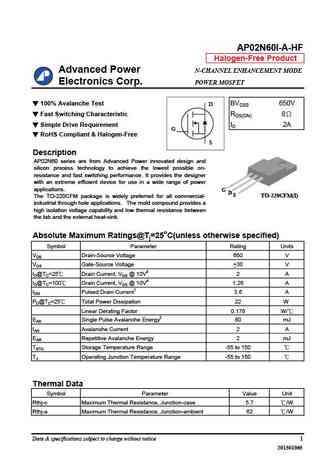
AP02N60I-A-HF Halogen-Free Product Advanced Power N-CHANNEL ENHANCEMENT MODE Electronics Corp. POWER MOSFET 100% Avalanche Test BVDSS 650V D Fast Switching Characteristic RDS(ON) 8 Simple Drive Requirement ID 2A G RoHS Compliant & Halogen-Free S Description AP02N60 series are from Advanced Power innovated design and silicon process technology to achieve the lowest
ap02n60t-h-hf.pdf
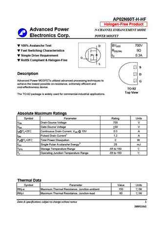
AP02N60T-H-HF Halogen-Free Product Advanced Power N-CHANNEL ENHANCEMENT MODE Electronics Corp. POWER MOSFET 100% Avalanche Test BVDSS 700V D Fast Switching Characteristics RDS(ON) 9 Simple Drive Requirement ID 0.3A G RoHS Compliant & Halogen-Free S S Description D Advanced Power MOSFETs utilized advanced processing techniques to G achieve the lowest possible o
ap02n60i-a-hf.pdf
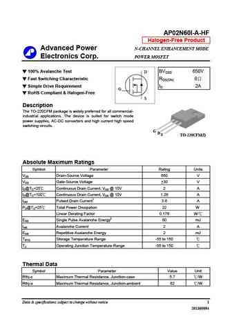
AP02N60I-A-HF Halogen-Free Product Advanced Power N-CHANNEL ENHANCEMENT MODE Electronics Corp. POWER MOSFET 100% Avalanche Test BVDSS 650V D Fast Switching Characteristic RDS(ON) 8 Simple Drive Requirement ID 2A G RoHS Compliant & Halogen-Free S Description The TO-220CFM package is widely preferred for all commercial- industrial applications. The device is suited
ap02n60h-h ap02n60j-h.pdf
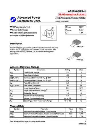
AP02N60H/J-H RoHS-compliant Product Advanced Power N-CHANNEL ENHANCEMENT MODE Electronics Corp. POWER MOSFET 100% Avalanche Test BVDSS 700V D Lower Gate Charge RDS(ON) 8.8 Fast Switching Characteristic ID 1.4A G Simple Drive Requirement S Description G D S TO-252(H) The TO-252 package is widely preferred for all commercial-industrial surface mount applications
ap02n60h-h-hf ap02n60j-h-hf.pdf
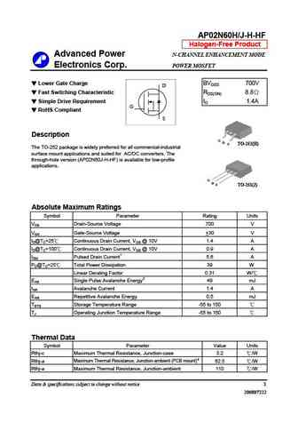
AP02N60H/J-H-HF Halogen-Free Product Advanced Power N-CHANNEL ENHANCEMENT MODE Electronics Corp. POWER MOSFET Lower Gate Charge BVDSS 700V D Fast Switching Characteristic RDS(ON) 8.8 Simple Drive Requirement ID 1.4A G RoHS Compliant S Description G D S TO-252(H) The TO-252 package is widely preferred for all commercial-industrial surface mount applications and
ap02n60h-hf ap02n60j-hf.pdf
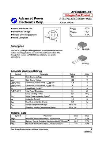
AP02N60H/J-HF Halogen-Free Product Advanced Power N-CHANNEL ENHANCEMENT MODE Electronics Corp. POWER MOSFET 100% Avalanche Test BVDSS 600V D Lower Gate Charge RDS(ON) 8 Simple Drive Requirement ID 1.6A G RoHS Compliant S Description G D TO-252(H) S The TO-252 package is widely preferred for all commercial-industrial surface mount applications and suited for AC
ftu02n60b ftd02n60b.pdf
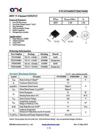
FTU02N60B/FTD02N60B 600V N-Channel MOSFET BVDSS RDS(ON) (Max.) ID General Features Low ON Resistance 600V 5.5 1.9A Low Gate Charge (typical 7.4nC) Fast Switching 100% Avalanche Tested RoHS Compliant Halogen-free available Applications High Efficiency SMPS Adaptor/Charger Active PFC LCD Panel Power Ordering Information
afn02n60t220ft afn02n60t220t afn02n60t251t.pdf
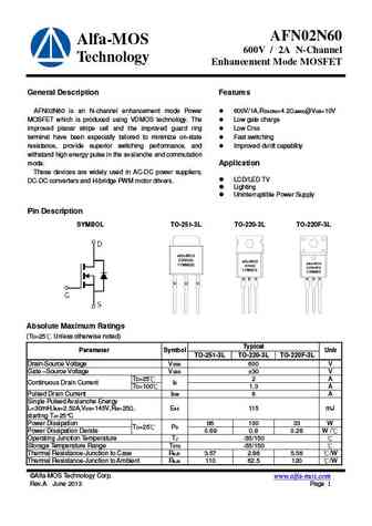
AFN02N60 Alfa-MOS 600V / 2A N-Channel Technology Enhancement Mode MOSFET General Description Features AFN02N60 is an N-channel enhancement mode Power 600V/1A,RDS(ON)=4.2 (MAX)@VGS=10V MOSFET which is produced using VDMOS technology. The Low gate charge improved planar stripe cell and the improved guard ring Low Crss terminal have been especially tailored to minimize on-state
afn12n60t220ft afn12n60t220t.pdf
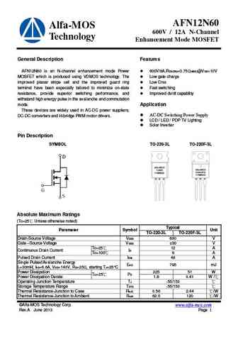
AFN12N60 Alfa-MOS 600V / 12A N-Channel Technology Enhancement Mode MOSFET General Description Features AFN12N60 is an N-channel enhancement mode Power 600V/6A,RDS(ON)=0.75 (MAX)@VGS=10V MOSFET which is produced using VDMOS technology. The Low gate charge improved planar stripe cell and the improved guard ring Low Crss terminal have been especially tailored to minimize on-sta
sss2n60.pdf
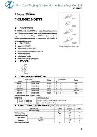
Shenzhen Tuofeng Semiconductor Technology Co., Ltd SSS2N60 2 Amps 600Volts 2 Amps 600Volts 2 Amps 600Volts 2 Amps 600Volts N-CHANNEL MOSFET N-CHANNEL MOSFET N-CHANNEL MOSFET N-CHANNEL MOSFET DESCRIPTION The SSS2N60 is a high voltage MOSFET and is designed to have better characteristics, such as fast switching time, low gate charge, low on-state resistance and have a high rug
sss12n60.pdf
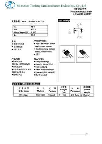
Shenzhen Tuofeng Semiconductor Technology Co., Ltd SSS12N60 N N-CHANNEL MOSFET Package MAIN CHARACTERISTICS 12 A ID 600 V VDSS Rdson 0.65 @Vgs=10V 39nC Qg APPLICATIONS High efficiency switch mode power supplies Electronic lamp ballasts UPS
sif2n60d.pdf
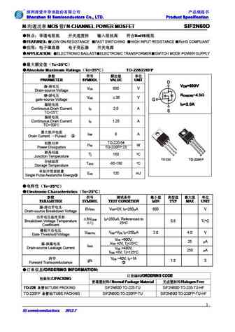
Shenzhen SI Semiconductors Co., LTD. Product Specification Shenzhen SI Semiconductors Co., LTD. Product Specification Shenzhen SI Semiconductors Co., LTD. Product Specification Shenzhen SI Semiconductors Co., LTD. Product Specification N- MOS / N-CHANNEL POWER MOSFET SIF2N60D N- MOS / N-CHANNEL POWER MOSFET SIF2N60D N
sif12n60c.pdf
Shenzhen SI Semiconductors Co., LTD. Product Specification Shenzhen SI Semiconductors Co., LTD. Product Specification Shenzhen SI Semiconductors Co., LTD. Product Specification Shenzhen SI Semiconductors Co., LTD. Product Specification N- MOS / N-CHANNEL POWER MOSFET SIF12N60C N- MOS / N-CHANNEL POWER MOSFET SIF12N60C
sif2n60d 1.pdf
Shenzhen SI Semiconductors Co., LTD. Product Specification Shenzhen SI Semiconductors Co., LTD. Product Specification Shenzhen SI Semiconductors Co., LTD. Product Specification Shenzhen SI Semiconductors Co., LTD. Product Specification N- MOS / N-CHANNEL POWER MOSFET SIF2N60D N- MOS / N-CHANNEL POWER MOSFET SIF2N60D N- MOS / N-CHANN
sif2n60c 1.pdf
Shenzhen SI Semiconductors Co., LTD. Product Specification Shenzhen SI Semiconductors Co., LTD. Product Specification Shenzhen SI Semiconductors Co., LTD. Product Specification Shenzhen SI Semiconductors Co., LTD. Product Specification N- MOS / N-CHANNEL POWER MOSFET SIF2N60C N- MOS / N-CHANNEL POWER MOSFET SIF2N60C N- MOS / N-CHANN
sif2n60c.pdf
Shenzhen SI Semiconductors Co., LTD. Product Specification Shenzhen SI Semiconductors Co., LTD. Product Specification Shenzhen SI Semiconductors Co., LTD. Product Specification Shenzhen SI Semiconductors Co., LTD. Product Specification N- MOS / N-CHANNEL POWER MOSFET SIF2N60C N- MOS / N-CHANNEL POWER MOSFET SIF2N60C N
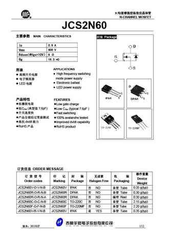
jcs2n60t jcs2n60v jcs2n60r jcs2n60c jcs2n60f.pdf
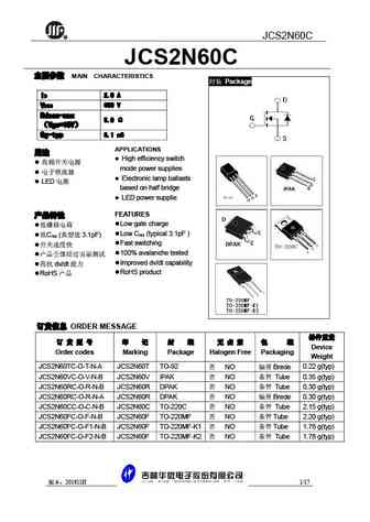
R JCS2N60C JCS2N60C MAIN CHARACTERISTICS Package ID 2.0 A VDSS 600 V Rdson-max 5.0 Vgs=10V Qg-typ 8.1 nC APPLICATIONS l High efficiency switch l mode power supplies l l Electronic lamp ballasts l LED based on half bridge l LED power supplie FEATURES l Low gate c
jcs2n60t jcs2n60mf jcs2n60v jcs2n60r jcs2n60c jcs2n60f.pdf
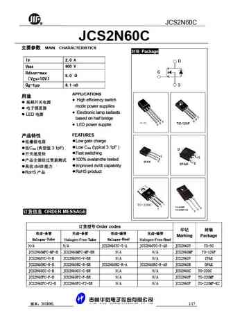
R JCS2N60C JCS2N60C MAIN CHARACTERISTICS Package ID 2.0 A VDSS 600 V Rdson-max 5.0 Vgs=10V Qg-typ 8.1 nC APPLICATIONS High efficiency switch mode power supplies Electronic lamp ballasts LED based on half bridge LED power supplie FEATURES
mp2n60er.pdf
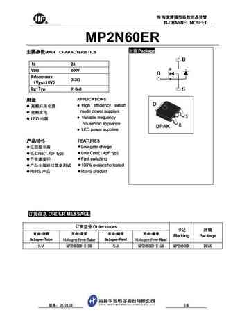
N R N-CHANNEL MOSFET MP2N60ER Package MAIN CHARACTERISTICS ID 2A VDSS 600V Rdson-max 3.3 Vgs=10V Qg-Typ 9.8nC APPLICATIONS High efficiency switch mode power supplies Variable frequency LED household appliance LED power supp
jcs12n60ct jcs12n60ft jcs12n60st jcs12n60bt.pdf
N R N-CHANNEL MOSFET JCS12N60T Package MAIN CHARACTERISTICS ID 12.0A VDSS 600 V Rdson-max 0.65 @Vgs=10V Qg 39 nC APPLICATIONS High efficiency switch mode power supplies Electronic lamp ballasts LED based on half bridge L
jcs2n60vb jcs2n60rb jcs2n60cb jcs2n60fb jcs2n60mb jcs2n60mfb.pdf
N R N-CHANNEL MOSFET JCS2N60B MAIN CHARACTERISTICS Package ID 2.0 A VDSS 600 V Rdson Vgs=10V 4.5 -MAX Qg-TYP 5.9nC APPLICATIONS High efficiency switch mode power supplies Electronic lamp ballasts LED based on half bridge
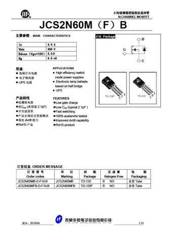
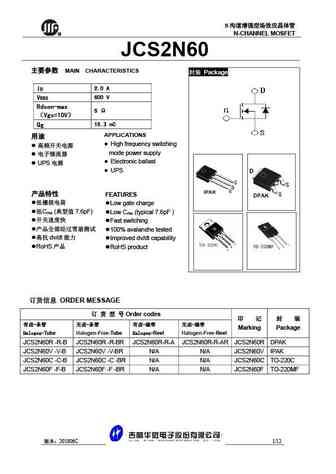
mtn12n60fp.pdf
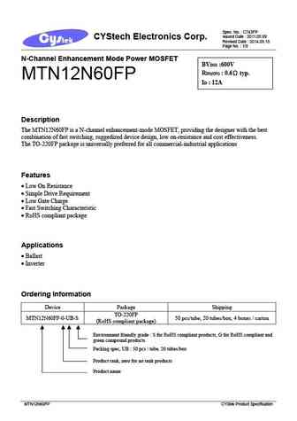
Spec. No. C743FP Issued Date 2011.05.09 CYStech Electronics Corp. Revised Date 2014.05.15 Page No. 1/9 N-Channel Enhancement Mode Power MOSFET BVDSS 600V RDS(ON) 0.6 typ. MTN12N60FP ID 12A Description The MTN12N60FP is a N-channel enhancement-mode MOSFET, providing the designer with the best combination of fast switching, ruggedized device design, low on-re
mtn12n60e3.pdf
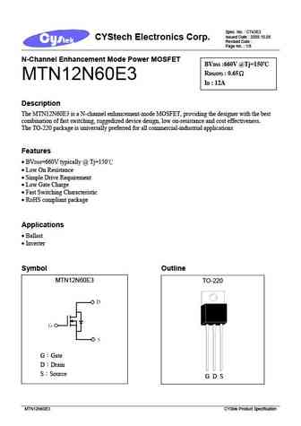
Spec. No. C743E3 Issued Date 2009.10.08 CYStech Electronics Corp. Revised Date Page No. 1/8 N-Channel Enhancement Mode Power MOSFET BVDSS 660V @Tj=150 C RDS(ON) 0.65 MTN12N60E3 ID 12A Description The MTN12N60E3 is a N-channel enhancement-mode MOSFET, providing the designer with the best combination of fast switching, ruggedized device design, low on-resist
mtn12n60bfp.pdf
Spec. No. C164FP Issued Date 2015.03.04 CYStech Electronics Corp. Revised Date Page No. 1/9 N-Channel Enhancement Mode Power MOSFET BVDSS 600V RDS(ON) 0.46 typ. MTN12N60BFP ID 12A Description The MTN12N60BFP is a N-channel enhancement-mode MOSFET, providing the designer with the best combination of fast switching, ruggedized device design, low on-resistanc
mtn2n60j3.pdf
Spec. No. C435J3 Issued Date 2009.01.20 CYStech Electronics Corp. Revised Date 2013.12.26 Page No. 1/11 N-Channel Enhancement Mode Power MOSFET BVDSS 600V RDS(ON) 4.0 (typ.) MTN2N60J3 ID 2A Description The MTN2N60J3 is a N-channel enhancement-mode MOSFET, providing the designer with the best combination of fast switching, ruggedized device design, low on-res
mtn2n60fp.pdf
Spec. No. C435FP Issued Date 2009.01.19 CYStech Electronics Corp. Revised Date 2011.03.30 Page No. 1/ 10 N-Channel Enhancement Mode Power MOSFET BVDSS 600V RDS(ON) 4.1 typ. MTN2N60FP ID 2A Description The MTN2N60FP is a N-channel enhancement-mode MOSFET, providing the designer with the best combination of fast switching, ruggedized device design, low on-r
mtn2n60i3.pdf
Spec. No. C435I3 Issued Date 2009.01.20 CYStech Electronics Corp. Revised Date 2011.11.10 Page No. 1/11 N-Channel Enhancement Mode Power MOSFET BVDSS 600V RDS(ON) 4.0 (typ.) MTN2N60I3 ID 2A Description The MTN2N60I3 is a N-channel enhancement-mode MOSFET, providing the designer with the best combination of fast switching, ruggedized device design, low on-res
12n60 12n60f.pdf
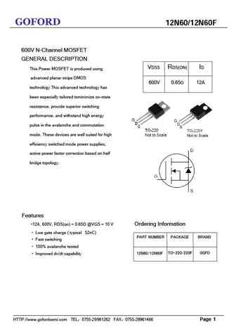
GOFORD 12N60/12N60F 600V N-Channel MOSFET GENERAL DESCRIPTION VDSS RDS(ON) ID This Power MOSFET is produced using advanced planar stripe DMOS 600V 0.65 12A technology.This advanced technology has been especially tailored tominimize on-state resistance, provide superior switching performance, and withstand high energy pulse in the avalanche and commutation mode. These devices are
sdu02n60 sdd02n60.pdf
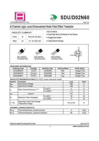
Green Product SDU/D02N60 a S mHop Microelectronics C orp. Ver 2.2 N-Channel Logic Level Enhancement Mode Field Effect Transistor FEATURES PRODUCT SUMMARY Super high dense cell design for low RDS(ON). VDSS ID RDS(ON) ( ) Max Rugged and reliable. 600V 2A 4.7 @ VGS=10V Suface Mount Package. D G S SDU SERIES SDD SERIES SDD SERIES TO-252(D-PAK) TO-251S(I-PAK) TO-251L(I-PAK) ORDERIN
ssf2n60.pdf
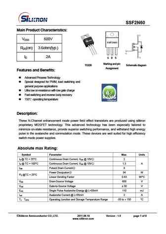
SSF2N60 Main Product Characteristics VDSS 600V RDS(on) 3.6ohm(typ.) ID 2A TO220 Marking and pin Schematic diagram Assignment Features and Benefits Advanced Process Technology Special designed for PWM, load switching and general purpose applications Ultra low on-resistance with low gate charge Fast switching and reverse body recovery 150 operating temper
ssf2n60f.pdf
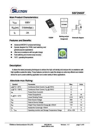
SSF2N60F Main Product Characteristics VDSS 600V RDS(on) 3.6ohm(typ.) ID 2A Marking a nd p in Sche ma ti c di agr a m TO220F Assignment Features and Benefits Advanced MOSFET process technology Special designed for PWM, load switching and general purpose applications Ultra low on-resistance with low gate charge Fast switching and reverse body recove
ssf12n60f.pdf
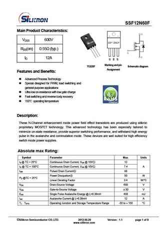
SSF12N60F Main Product Characteristics VDSS 600V RDS(on) 0.55 (typ.) ID 12A Sche ma ti c di agr a m TO220F Marking and pin Assignment Features and Benefits Advanced Process Technology Special designed for PWM, load switching and general purpose applications Ultra low on-resistance with low gate charge Fast switching and reverse body recovery
ssf2n60d.pdf
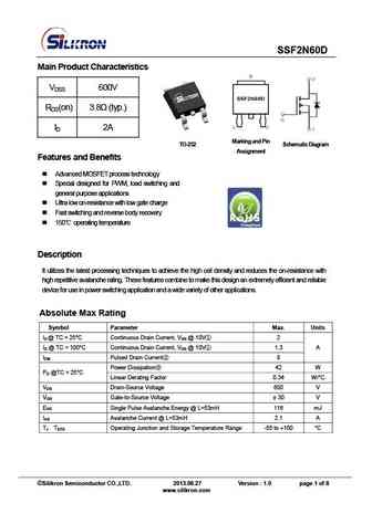
SSF2N60D Main Product Characteristics VDSS 600V RDS(on) 3.8 (typ.) ID 2A Marking and P in S che ma ti c Diag r am TO-252 Assignment Features and Benefits Advanced MOSFET process technology Special designed for PWM, load switching and general purpose applications Ultra low on-resistance with low gate charge Fast switching and reverse body recovery
ssf2n60g.pdf

SSF2N60G Main Product Characteristics VDSS 600V RDS(on) 3.5 (typ.) ID 2A TO-251 Marking and p in S che ma ti c di ag ra m Assignment Features and Benefits Advanced MOSFET process technology Special designed for PWM, load switching and general purpose applications Ultra low on-resistance with low gate charge Fast switching and reverse body recovery
ssf2n60d2.pdf
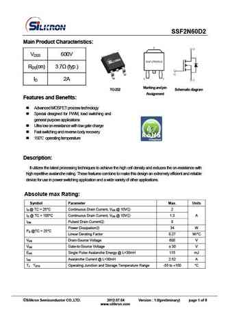
SSF2N60D2 Main Product Characteristics VDSS 600V RDS(on) 3.7 (typ.) ID 2A TO-252 Marking a nd pin Sche ma ti c di agr a m Assignment Features and Benefits Advanced MOSFET process technology Special designed for PWM, load switching and general purpose applications Ultra low on-resistance with low gate charge Fast switching and reverse body recovery
cs2n60 to-252.pdf
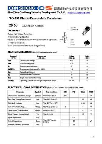
ShenZhen CanSheng Industry Development Co.,Ltd ShenZhen CanSheng Industry Development Co.,Ltd ShenZhen CanSheng Industry Development Co.,Ltd www.szcansheng.com ShenZhen CanSheng Industry Development Co.,Ltd. TO-252 Plastic-Encapsulate Transistors TO-252 Plastic-Encapsulate Transistors TO-252 Plastic-Encapsulate Transistors TO-252 Plastic-Encapsula
ftp02n60c fta02n60c.pdf
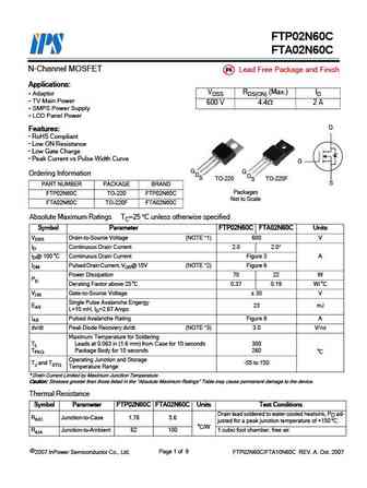
FTP02N60C FTA02N60C N-Channel MOSFET Pb Lead Free Package and Finish Applications VDSS RDS(ON) (Max.) ID Adaptor TV Main Power 600 V 4.4 2 A SMPS Power Supply LCD Panel Power D Features RoHS Compliant Low ON Resistance Low Gate Charge Peak Current vs Pulse Width Curve G G G Ordering Information DS DS TO-220F TO-220 S PART NUMBER PA
ftd02n60c ftu02n60c.pdf
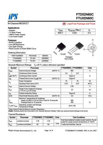
FTD02N60C FTU02N60C N-Channel MOSFET Pb Lead Free Package and Finish Applications VDSS RDS(ON) (Max.) ID Adaptor TV Main Power 600 V 4.4 2 A SMPS Power Supply LCD Panel Power D Features RoHS Compliant Low ON Resistance Low Gate Charge Peak Current vs Pulse Width Curve G G G Ordering Information DS DS TO-251 TO-252 S PART NUMBER PAC
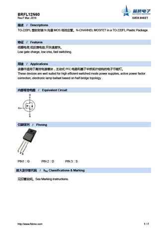
bra2n60.pdf
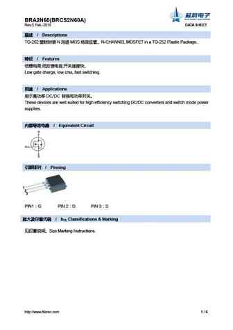
BRA2N60(BRCS2N60A) Rev.C Feb.-2015 DATA SHEET / Descriptions TO-262 N MOS N-CHANNEL MOSFET in a TO-252 Plastic Package.. / Features , , Low gate charge, low crss, fast switching. / Applications DC/DC These devices are well suited for high
br2n60.pdf
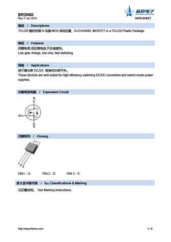
BR2N60 Rev. F Jul.-2018 DATA SHEET / Descriptions TO-220 N MOS N-CHANNEL MOSFET in a TO-220 Plastic Package. / Features , , Low gate charge, low crss, fast switching. / Applications DC/DC These devices are well suited for high efficiency
brd2n60.pdf
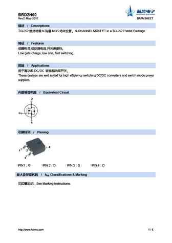
BRD2N60 Rev.D May.-2016 DATA SHEET / Descriptions TO-252 N MOS N-CHANNEL MOSFET in a TO-252 Plastic Package. / Features , , Low gate charge, low crss, fast switching. / Applications DC/DC These devices are well suited for high efficiency
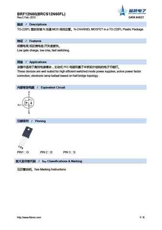
bri2n60.pdf
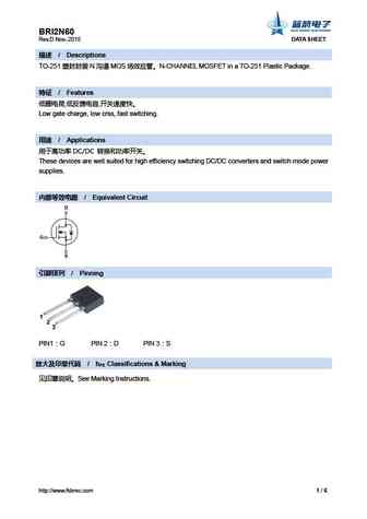
BRI2N60 Rev.D Nov.-2015 DATA SHEET / Descriptions TO-251 N MOS N-CHANNEL MOSFET in a TO-251 Plastic Package. / Features , , Low gate charge, low crss, fast switching. / Applications DC/DC These devices are well suited for high efficiency
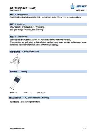
brf2n60.pdf
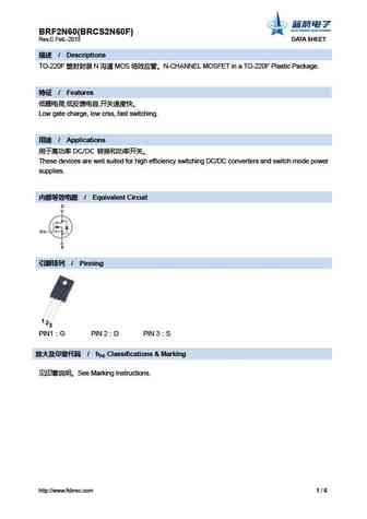
BRF2N60(BRCS2N60F) Rev.C Feb.-2015 DATA SHEET / Descriptions TO-220F N MOS N-CHANNEL MOSFET in a TO-220F Plastic Package. / Features , , Low gate charge, low crss, fast switching. / Applications DC/DC These devices are well suited for hi
brl2n60.pdf
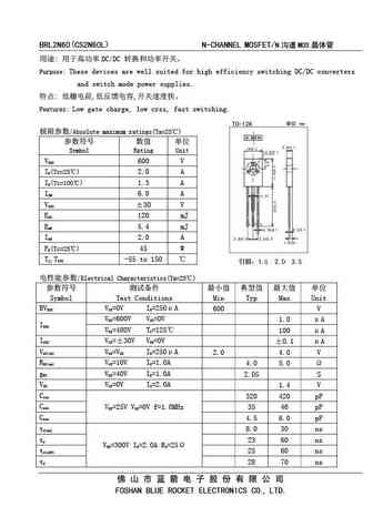
BRL2N60(CS2N60L) N-CHANNEL MOSFET/N MOS DC/DC Purpose These devices are well suited for high efficiency switching DC/DC converters and switch mode power supplies. , , Features Low gate charge, low crss, fast switching. /Absolute maximum ratings(Ta=25
l2n60d l2n60f l2n60i l2n60p.pdf
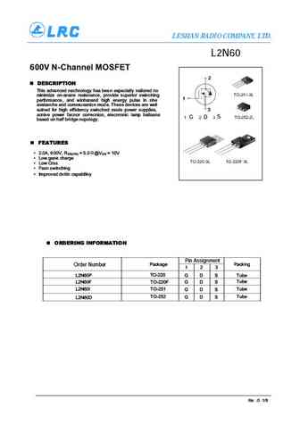
LESHAN RADIO COMPANY, LTD. L2N60 600V N-Channel MOSFET 2 DESCRIPTION 1 3
l2n600.pdf
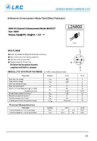
LESHAN RADIO COMPANY, LTD. 600V N-Channel Enhancement-Mode MOSFET VDS= 600V RDS(ON), Vgs@10V, Ids@1A = 3.8 We declare that the material of product compliance with RoHS requirements. 1/5 LESHAN RADIO COMPANY, LTD. L2N600 Electrical Characteristics Tc = 25 C unless otherwise noted Parameter Symbol Test Condition Min Typ Max Unit Off Characteristics Drain-Source Breakdown Voltage
2n60a 2n60af 2n60g.pdf
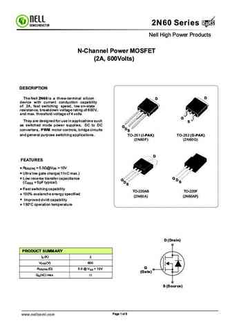
RoHS 2N60 Series RoHS SEMICONDUCTOR Nell High Power Products N-Channel Power MOSFET (2A, 600Volts) DESCRIPTION D The Nell 2N60 is a three-terminal silicon D device with current conduction capability of 2A, fast switching speed, low on-state resistance, breakdown voltage rating of 600V, and max. threshold voltage of 4 volts. G They are designed for use in applications such
12n60a 12n60af.pdf
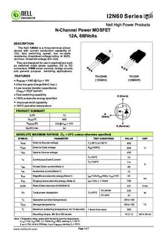
RoHS I2N60 Series RoHS SEMICONDUCTOR Nell High Power Products N-Channel Power MOSFET 12A, 600Volts DESCRIPTION The Nell 12N60 is a three-terminal silicon device with current conduction capability of D 12A, fast switching speed, low on-state resistance, breakdown voltage rating of 600V, and max. threshold voltage of 4 volts. They are designed for use in applications such as s
hfh12n60.pdf
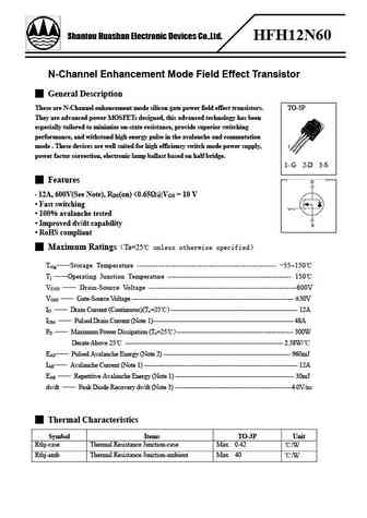
Shantou Huashan Electronic Devices Co.,Ltd. HFH12N60 N-Channel Enhancement Mode Field Effect Transistor General Description These are N-Channel enhancement mode silicon gate power field effect transistors. TO-3P They are advanced power MOSFETs designed, this advanced technology has been especially tailored to minimize on-state resistance, provide superior switching performanc
hff2n60.pdf
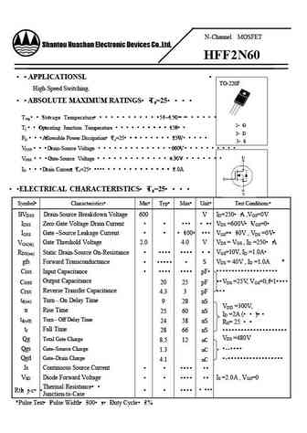
N-Channel MOSFET Shantou Huashan Electronic Devices Co.,Ltd. HFF2N60 APPLICATIONSL TO-220F High-Speed Switching. ABSOLUTE MAXIMUM RATINGS Ta=25 Tstg Storage Temperature -55 150 1 G Tj Operating Junction Temperature 150 2 D PD Allowable Power Dissipation Tc=25
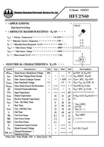
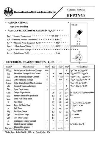
cs12n60 a8r.pdf
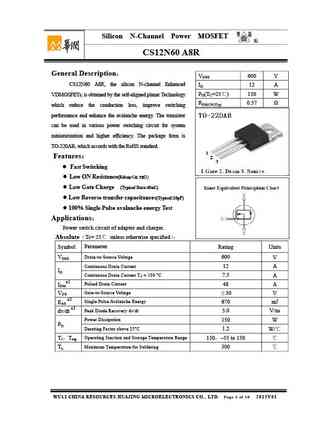
Silicon N-Channel Power MOSFET R CS12N60 A8R General Description VDSS 600 V CS12N60 A8R, the silicon N-channel Enhanced ID 12 A PD(TC=25 ) 150 W VDMOSFETs, is obtained by the self-aligned planar Technology RDS(ON)Typ 0.57 which reduce the conduction loss, improve switching performance and enhance the avalanche energy. The transistor can be used in various po
cs12n60f a9r.pdf

Silicon N-Channel Power MOSFET R CS12N60F A9R General Description VDSS 600 V CS12N60F A9R, the silicon N-channel Enhanced ID 12 A PD(TC=25 ) 42 W VDMOSFETs, is obtained by the self-aligned planar Technology RDS(ON)Typ 0.57 which reduce the conduction loss, improve switching performance and enhance the avalanche energy. The transistor can be used in various p
cs2n60 a7h.pdf
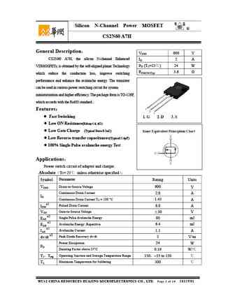
Silicon N-Channel Power MOSFET R CS2N60 A7H General Description VDSS 600 V CS2N60 A7H, the silicon N-channel Enhanced ID 2 A PD (TC=25 ) 24 W VDMOSFETs, is obtained by the self-aligned planar Technology RDS(ON)Typ 3.6 which reduce the conduction loss, improve switching performance and enhance the avalanche energy. The transistor can be used in various power
cs2n60f a9h.pdf

Silicon N-Channel Power MOSFET R CS2N60F A9H General Description VDSS 600 V CS2N60F A9H, the silicon N-channel Enhanced ID 2 A PD (TC=25 ) 24 W VDMOSFETs, is obtained by the self-aligned planar Technology RDS(ON)Typ 3.6 which reduce the conduction loss, improve switching performance and enhance the avalanche energy. The transistor can be used in various pow
cs2n60 a3h.pdf
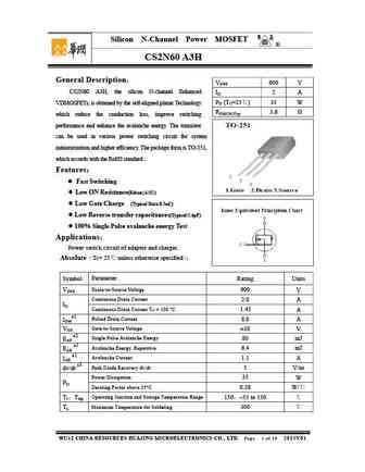
Silicon N-Channel Power MOSFET R CS2N60 A3H General Description VDSS 600 V CS2N60 A3H, the silicon N-channel Enhanced ID 2 A PD (TC=25 ) 35 W VDMOSFETs, is obtained by the self-aligned planar Technology RDS(ON)Typ 3.6 which reduce the conduction loss, improve switching performance and enhance the avalanche energy. The transistor can be used in various power
cs2n60 a4h.pdf
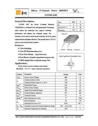
Silicon N-Channel Power MOSFET R CS2N60 A4H General Description VDSS 600 V CS2N60 A4H, the silicon N-channel Enhanced ID 2 A PD (TC=25 ) 35 W VDMOSFETs, is obtained by the self-aligned planar Technology RDS(ON)Typ 3.6 which reduce the conduction loss, improve switching performance and enhance the avalanche energy. The transistor can be used in various power
cs12n60f a9hd.pdf

Silicon N-Channel Power MOSFET R CS12N60F A9HD VDSS 600 V General Description ID 12 A CS12N60F A9HD, the silicon N-channel Enhanced PD (TC=25 ) 55 W VDMOSFETs, is obtained by the self-aligned planar RDS(ON)Typ 0.5 Technology which reduce the conduction loss, improve switching performance and enhance the avalanche energy. The transistor can be used in vario
cs2n60 a4t.pdf

Silicon N-Channel Power MOSFET R CS2N60 A4T General Description VDSS 600 V CS2N60 A4T, the silicon N-channel Enhanced ID 2 A PD (TC=25 ) 35 W VDMOSFETs, is obtained by the self-aligned planar Technology RDS(ON)Typ 3.5 which reduce the conduction loss, improve switching performance and enhance the avalanche energy. The transistor can be used in various power
cs12n60 a8h.pdf
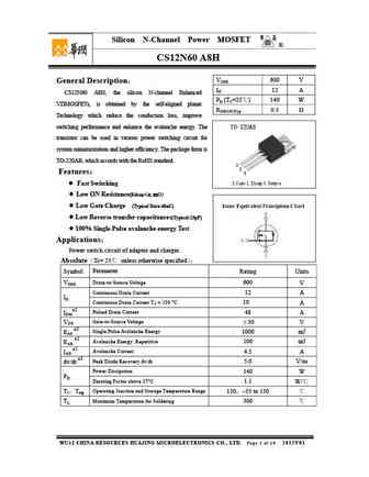
Silicon N-Channel Power MOSFET R CS12N60 A8H VDSS 600 V General Description ID 12 A CS12N60 A8H, the silicon N-channel Enhanced PD (TC=25 ) 140 W VDMOSFETs, is obtained by the self-aligned planar RDS(ON)Typ 0.5 Technology which reduce the conduction loss, improve switching performance and enhance the avalanche energy. The transistor can be used in various po
cs12n60 a8hd.pdf

Silicon N-Channel Power MOSFET R CS12N60 A8HD VDSS 600 V XGeneral Description ID 12 A CS12N60 A8HD, the silicon N-channel Enhanced PD (TC=25 ) 140 W VDMOSFETs, is obtained by the self-aligned planar RDS(ON)Typ 0.5 Technology which reduce the conduction loss, improve switching performance and enhance the avalanche energy. The transistor can be used in various
cs12n60f a9h.pdf
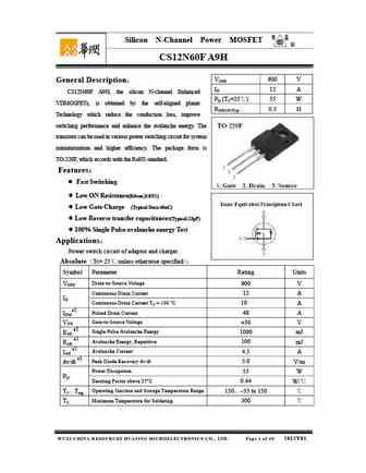
Silicon N-Channel Power MOSFET R CS12N60F A9H VDSS 600 V General Description ID 12 A CS12N60F A9H, the silicon N-channel Enhanced PD (TC=25 ) 55 W VDMOSFETs, is obtained by the self-aligned planar RDS(ON)Typ 0.5 Technology which reduce the conduction loss, improve switching performance and enhance the avalanche energy. The transistor can be used in various
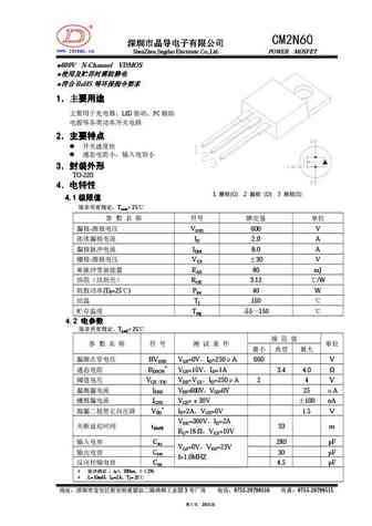
cm12n60a to220a.pdf
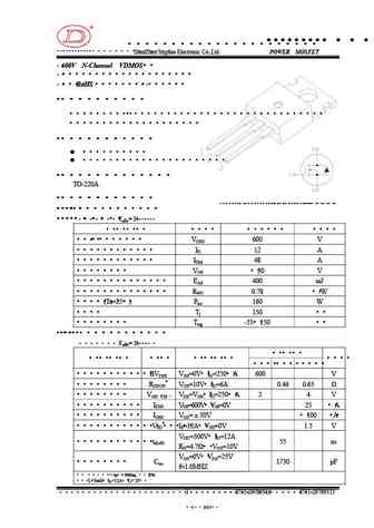
R CM12N60A www.jdsemi.cn ShenZhen Jingdao Electronic Co.,Ltd. POWER MOSFET 600V N-Channel VDMOS RoHS 1 LD E 2 3
cm12n60af.pdf
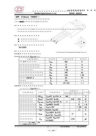
R CM12N60AF www.jdsemi.cn ShenZhen Jingdao Electronic Co.,Ltd. POWER MOSFET 600V N-Channel VDMOS RoHS 1 LD E 2 1
cm2n60c to251.pdf
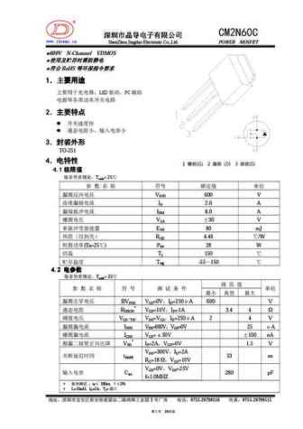
R CM2N60C www.jdsemi.cn ShenZhen Jingdao Electronic Co.,Ltd. POWER MOSFET 600V N-Channel VDMOS RoHS
cm2n60f.pdf
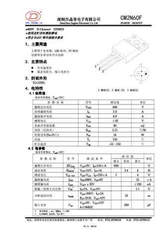
R CM2N60F www.jdsemi.cn ShenZhen Jingdao Electronic Co.,Ltd. POWER MOSFET 600V N-Channel VDMOS RoHS
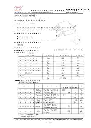
kqb2n60.pdf
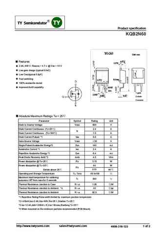
SMD Type IC SMD Type IC SMD Type IC SMD Type IC SMD Type IC SMD Type Transistors SMD Type Transistors SMD Type Transistors SMD Type Transistors SMD Type Transistors SMD Type Transistors SMD Type Transistors SMD Type SMD Type SMD Type SMD Type SMD Type SMD Type SMD Type SMD Type SMD Type SMD Type SMD Type SMD Type SMD Type IC SMD Type IC Product specification KQB2N60
ftk2n60p f d i.pdf
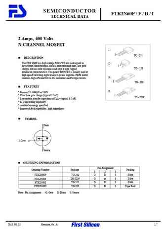
SEMICONDUCTOR FTK2N60P / F / D / I TECHNICAL DATA 2 Amps, 600 Volts N-CHANNEL MOSFET I 1 TO - 251 DESCRIPTION The FTK 2N60 is a high voltage MOSFET and is designed to D have better characteristics, such as fast switching time, low gate 1 TO - 252 charge, low on-state resistance and have a high rugged avalanche characteristics. This power MOSFET is usually used at high sp
d2n60.pdf
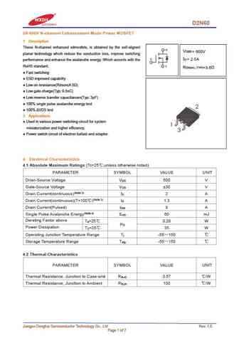
D2N60 2A 600V N-channel Enhancement Mode Power MOSFET 1 Description These N-channel enhanced vdmosfets, is obtained by the self-aligned V DSS = 600V planar technology which reduce the conduction loss, improve switching I = 2.0A D performance and enhance the avalanche energy. Which accords with the RoHS standard. R DS(on) TYP) =3.6 Fast switching ESD improved capabilit
f12n60.pdf
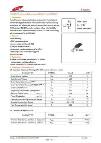
F12N60 12A 600V N-channel Enhancement Mode Power MOSFET 1 Description These N-channel enhanced vdmosfets, is obtained by the self-aligned V DSS = 600V planar technology which reduce the conduction loss, improve switching I = 12.0A D performance and enhance the avalanche energy. Which accords with the RoHS standard. TO-220F provides insulation voltage rated at 2000V R DS(on) TYP)
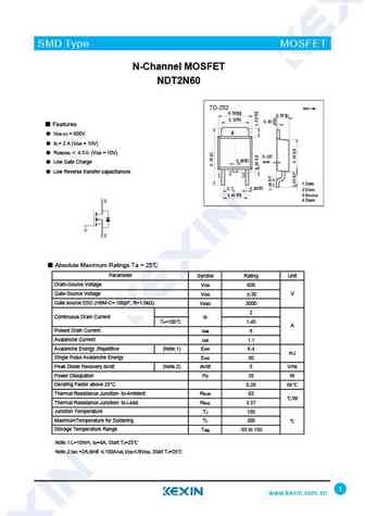
ndt2n60p.pdf
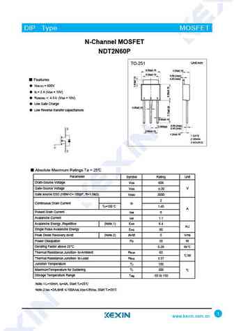
DIP Type MOSFET N-Channel MOSFET NDT2N60P Unit mm TO-251 6.50 0.15 2.30 0.10 5.30 0.10 0.58 (max) 0.43 (min) Features VDS (V) = 600V ID = 2 A (VGS = 10V) RDS(ON) 4.5 (VGS = 10V) 1 2 3 Low Gate Charge 0.80 0.10 Low Reverse transfer capacitances 0.60 0.10 0.58 (max) 2.30(typ) 0.43 (min) 4.60 0.10 1.20 0.15 Absolute Maximum Ratin
svf2n60m svf2n60mj svf2n60nf svf2n60f svf2n60d.pdf
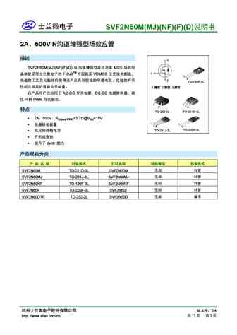
SVF2N60M(MJ)(NF)(F)(D) 2A 600V N 2 SVF2N60M(MJ)(NF)(F)(D) N MOS 1 F-CellTM VDMOS 1 2 3 3 TO-126F-3L
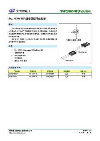
svf2n60rd svf2n60rm svf2n60rmj.pdf
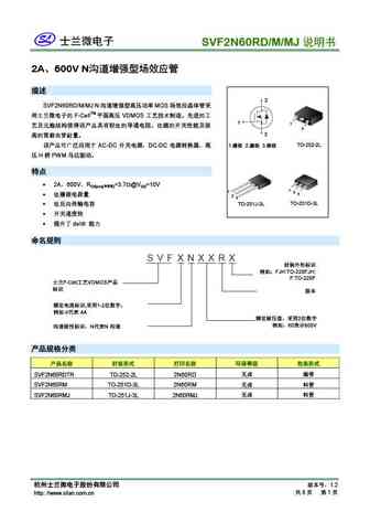
SVF2N60RD/M/MJ 2A 600V N 2 SVF2N60RD/M/MJ N MOS F-CellTM VDMOS 1 1 3 3
svf2n60m-f-t-d.pdf

SVF2N60M/F/T/D_Datasheet 2A, 600V N-CHANNEL MOSFET GENERAL DESCRIPTION SVF2N60M/F/T/D is an N-channel enhancement mode power MOS field effect transistor which is produced using Silan proprietary F-cellTM structure DMOS technology. The improved planar stripe cell and the improved guard ring terminal have been especially tailored to minimize on-state resistance, provide superior s
svd2n60.pdf
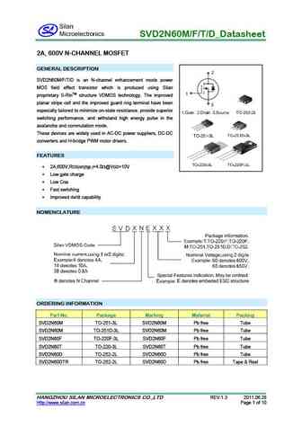
SVD2N60M/F/T/D_Datasheet 2A, 600V N-CHANNEL MOSFET GENERAL DESCRIPTION SVD2N60M/F/T/D is an N-channel enhancement mode power MOS field effect transistor which is produced using Silan proprietary S-RinTM structure VDMOS technology. The improved planar stripe cell and the improved guard ring terminal have been especially tailored to minimize on-state resistance, provide superior s
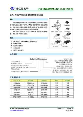
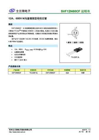
svf12n60cfj.pdf
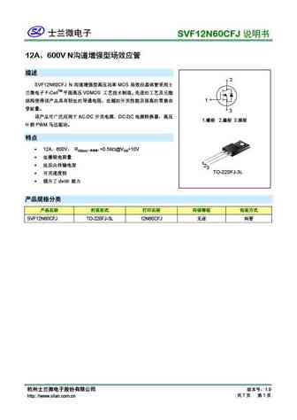
SVF12N60CFJ 12A 600V N 2 SVF12N60CFJ N MOS F-CellTM VDMOS 1 3
svf2n60cn svf2n60cm svf2n60cf.pdf
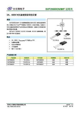
SVF2N60CN/M/F 2A 600V N 2 SVF2N60CN/M/F N MOS F-CellTM VDMOS 1 3 1. 2. 3
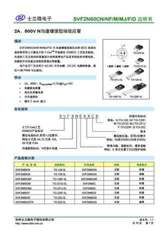
svf2n60m svf2n60mj svf2n60n svf2n60nf svf2n60f svf2n60t svf2n60d.pdf
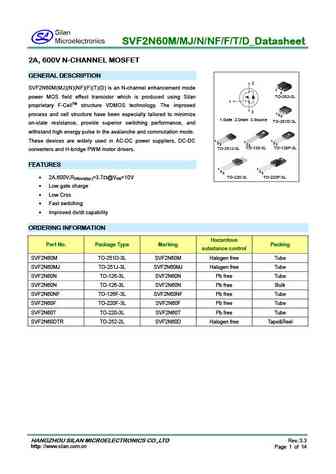
SVF2N60M/MJ/N/NF/F/T/D_Datasheet 2A, 600V N-CHANNEL MOSFET GENERAL DESCRIPTION 2 SVF2N60M(MJ)(N)(NF)(F)(T)(D) is an N-channel enhancement mode 1 3 TO-252-2L power MOS field effect transistor which is produced using Silan 1 proprietary F-CellTM structure VDMOS technology. The improved 3 1 process and cell structure have been especially tailored to minimize 2 3 1.Gate 2.Dra
svf2n60rdtr svf2n60rm svf2n60rmj.pdf
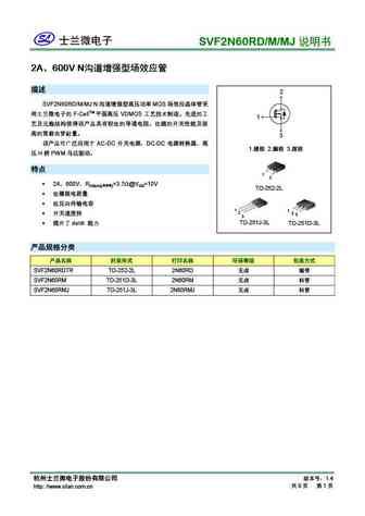
SVF2N60RD/M/MJ 2A 600V N 2 SVF2N60RD/M/MJ N MOS F-CellTM VDMOS 1 3
svf2n60m svf2n60f svf2n60t svf2n60d.pdf
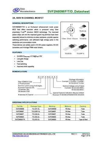
SVF2N60M/F/T/D_Datasheet 2A, 600V N-CHANNEL MOSFET GENERAL DESCRIPTION SVF2N60M/F/T/D is an N-channel enhancement mode power MOS field effect transistor which is produced using Silan proprietary F-cellTM structure DMOS technology. The improved planar stripe cell and the improved guard ring terminal have been especially tailored to minimize on-state resistance, provide superior s
svf12n60f svf12n60s svf12n60str svf12n60k.pdf
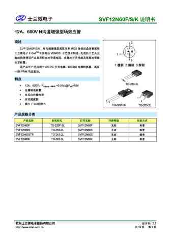
SVF12N60F/S/K 12A 600V N 2 SVF12N60F/S/K N MOS F-CellTM VDMOS 1 3 1. 2. 3
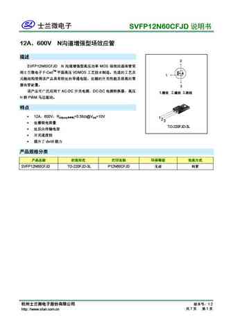
svf12n60t svf12n60f svf12n60s svf12n60k.pdf
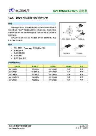
SVF12N60T/F/S/K 12A 600V N SVF12N60T/F/S/K N MOS F-CellTM VDMOS AC-DC
mdis2n60th.pdf
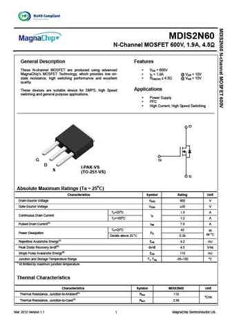
MDIS2N60 N-Channel MOSFET 600V, 1.9A, 4.5 General Description Features These N-channel MOSFET are produced using advanced VDS = 600V MagnaChip s MOSFET Technology, which provides low on- ID = 1.9A @ VGS = 10V state resistance, high switching performance and excellent RDS(ON) 4.5 @ VGS = 10V quality. Applications These devices are suitable device for SM
mdf2n60bth.pdf
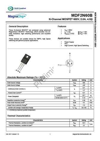
MDF2N60B N-Channel MOSFET 600V, 2.0A, 4.5 General Description Features These N-channel MOSFET are produced using advanced VDS = 600V MagnaChip s MOSFET Technology, which provides low on- ID = 2.0A @ VGS = 10V state resistance, high switching performance and excellent RDS(ON) 4.5 @ VGS = 10V quality. Applications These devices are suitable device for SMP
mdf2n60th mdf2n60tp mdp2n60th mdp2n60tp.pdf
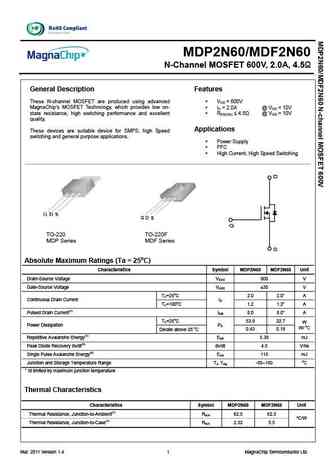
MDP2N60/MDF2N60 N-Channel MOSFET 600V, 2.0A, 4.5 General Description Features These N-channel MOSFET are produced using advanced V = 600V DS MagnaChip s MOSFET Technology, which provides low on- I = 2.0A @ V = 10V D GS state resistance, high switching performance and excellent R 4.5 @ V = 10V DS(ON) GS quality. Applications These devices are suitable device for SM
mdd2n60rh mdi2n60.pdf
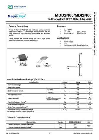
MDD2N60/MDI2N60 N-Channel MOSFET 600V, 1.9A, 4.5 General Description Features These N-channel MOSFET are produced using advanced V = 600V DS MagnaChip s MOSFET Technology, which provides low on- I = 1.9A @ V = 10V D GS state resistance, high switching performance and excellent R 4.5 @ V = 10V DS(ON) GS quality. Applications These devices are suitable device for
ms12n60.pdf
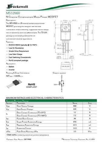
MS12N60 N-Channel Enhancement Mode Power MOSFET Description The MS12N60 is a N-channel enhancement-mode MOSFET, providing the designer with the best combination of fast switching, ruggedized device design, low on-resistance and cost effectiveness. The TO-220 package is universally preferred for all commercial-industrial applications Features BVDSS=6600V typically @ Tj=15
msq2n60.pdf
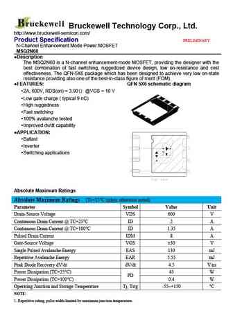
Bruckewell Technology Corp., Ltd. http //www.bruckewell-semicon.com/ Product Specification PRELIMINARY N-Channel Enhancement Mode Power MOSFET MSQ2N60 Description The MSQ2N60 is a N-channel enhancement-mode MOSFET, providing the designer with the best combination of fast switching, ruggedized device design, low on-resistance and cost effectiveness. The QFN-5X6 package which
msf2n60.pdf
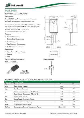
MSF2N60 600V N-Channel MOSFET Description The MSF2N60 is a N-channel enhancement-mode MOSFET , providing the designer with the best combination of fast switching, ruggedized device design, low on-resistance and cost effectiveness. The TO-220F package is universally preferred for all commercial-industrial applications Features Low On Resistance Simple Drive Requirem
msu2n60s.pdf
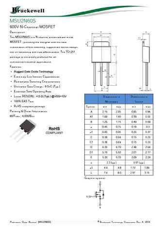
MSU2N60S 600V N-Channel MOSFET Description The MSU2N60S is a N-channel enhancement-mode MOSFET , providing the designer with the best combination of fast switching, ruggedized device design, low on-resistance and cost effectiveness. The TO-251 package is universally preferred for all commercial-industrial applications Features Rugged Gate Oxide Technology Extremely
msd2n60.pdf
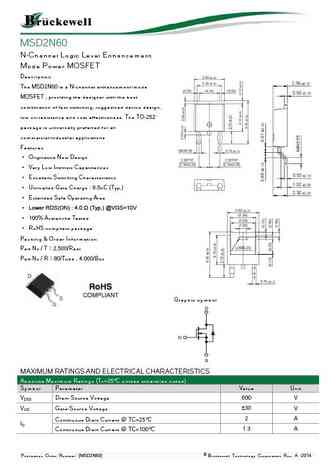
MSD2N60 N-Channel Logic Level Enhancement Mode Power MOSFET Description The MSD2N60 is a N-channel enhancement-mode MOSFET , providing the designer with the best combination of fast switching, ruggedized device design, low on-resistance and cost effectiveness. The TO-252 package is universally preferred for all commercial-industrial applications Features Originative Ne
msf12n60.pdf
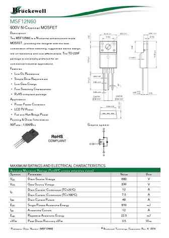
MSF12N60 600V N-Channel MOSFET Description The MSF12N60 is a N-channel enhancement-mode MOSFET , providing the designer with the best combination of fast switching, ruggedized device design, low on-resistance and cost effectiveness. The TO-220F package is universally preferred for all commercial-industrial applications Features Low On Resistance Simple Drive Requir
wfp2n60b.pdf
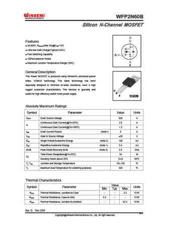
WFP2N60B WFP2N60B WFP2N60B WFP2N60B Silicon N-Channel MOSFET Silicon N-Channel MOSFET Silicon N-Channel MOSFET Silicon N-Channel MOSFET Features 2A,600V, R (Max 5 )@V =10V DS(on) GS Ultra-low Gate Charge(Typical 9.0nC) Fast Switching Capability 100%Avalanche Tested Maximum Junction Temperature Range(150 ) General Description This Power MOSFET is produced u
wff2n60b.pdf
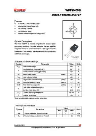
WFF2N60B WFF2N60B WFF2N60B WFF2N60B Silicon N-Channel MOSFET Silicon N-Channel MOSFET Silicon N-Channel MOSFET Silicon N-Channel MOSFET Features 2A,600V,R (Max 5.0 )@V =10V DS(on) GS Ultra-low Gate Charge(Typical 9nC) Fast Switching Capability 100%Avalanche Tested Maximum Junction Temperature Range(150 ) General Description This Power MOSFET is produced u
wff12n60.pdf
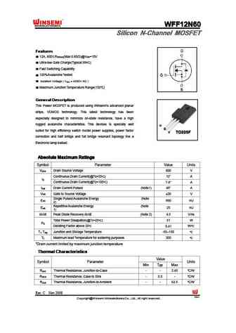
WFF12N60 WFF12N60 WFF12N60 WFF12N60 Silicon N-Channel MOSFET Silicon N-Channel MOSFET Silicon N-Channel MOSFET Silicon N-Channel MOSFET Features Features Features Features 12A, 600V,R (Max 0.65 )@V =10V DS(on) GS Ultra-low Gate Charge(Typical 39nC) Fast Switching Capability 100%Avalanche Tested Isolation Voltage ( V = 4000V AC ) ISO Maximum Junction T
wfp12n60.pdf
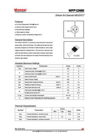
WFP12N60 WFP12N60 WFP12N60 WFP12N60 Silicon N-Channel MOSFET Features 12A, 600V,R (Max 0.65 )@V =10V DS(on) GS Ultra-low Gate Charge(Typical 43nC) Fast Switching Capability 100%Avalanche Tested Maximum Junction Temperature Range(150 ) General Description This Power MOSFET is produced using Winsemi s advanced planar stripe, DMOS technology. This latest tech
wff2n60.pdf
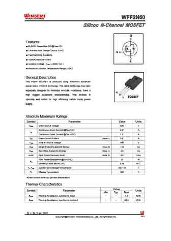
WFF2N60 WFF2N60 WFF2N60 WFF2N60 Silicon N-Channel MOSFET Silicon N-Channel MOSFET Silicon N-Channel MOSFET Silicon N-Channel MOSFET Features 2A,600V, R (Max 5 )@V =10V DS(on) GS Ultra-low Gate Charge(Typical 9.0nC) Fast Switching Capability 100%Avalanche Tested Isolation Voltage ( V = 4000V AC ) ISO Maximum Junction Temperature Range(150 ) General Desc
wfd2n60.pdf
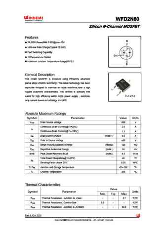
WFD2N60 WFD2N60 WFD2N60 WFD2N60 Silicon N-Channel MOSFET Silicon N-Channel MOSFET Silicon N-Channel MOSFET Silicon N-Channel MOSFET Features 2A,600V,R (Max 5.0 )@V =10V DS(on) GS Ultra-low Gate Charge(Typical 15.3nC) Fast Switching Capability 100%Avalanche Tested Maximum Junction Temperature Range(150 ) General Description This Power MOSFET is produced us
wfp2n60.pdf
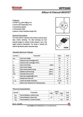
WFP2N60 WFP2N60 WFP2N60 WFP2N60 Silicon N-Channel MOSFET Silicon N-Channel MOSFET Silicon N-Channel MOSFET Silicon N-Channel MOSFET Features 2A,600V, RDS(on)(Max 5 )@VGS=10V Ultra-low Gate Charge(Typical 15nC) Fast Switching Capability 100%Avalanche Tested Maximum Junction Temperature Range(150 ) General Description This Power MOSFET is produced using Wins
wfu2n60b.pdf
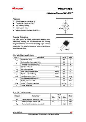
WFU2N60B WFU2N60B WFU2N60B WFU2N60B Silicon N-Channel MOSFET Silicon N-Channel MOSFET Silicon N-Channel MOSFET Silicon N-Channel MOSFET Features 2A,600V,R (Max 5.0 )@V =10V DS(on) GS Ultra-low Gate Charge(Typical 9nC) Fast Switching Capability 100%Avalanche Tested Maximum Junction Temperature Range(150 ) General Description This Power MOSFET is produced u
wfd2n60b.pdf
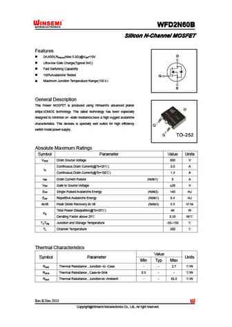
WFD2N60B WFD2N60B WFD2N60B WFD2N60B Silicon N-Channel MOSFET Silicon N-Channel MOSFET Silicon N-Channel MOSFET Silicon N-Channel MOSFET Features 2A,600V,R (Max 5.0 )@V =10V DS(on) GS Ultra-low Gate Charge(Typical 9nC) Fast Switching Capability 100%Avalanche Tested Maximum Junction Temperature Range(150 ) General Description This Power MOSFET is produced u
wfu2n60.pdf
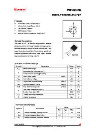
WFU2N60 WFU2N60 WFU2N60 WFU2N60 Silicon N-Channel MOSFET Silicon N-Channel MOSFET Silicon N-Channel MOSFET Silicon N-Channel MOSFET Features 2A,600V,R (Max 5.0 )@V =10V DS(on) GS Ultra-low Gate Charge(Typical 15.3nC) Fast Switching Capability 100%Avalanche Tested Maximum Junction Temperature Range(150 ) General Description This Power MOSFET is produced us
bl12n60-p bl12n60-a.pdf
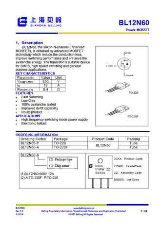
BL12N60 Power MOSFET Power MOSFET Power MOSFET Power MOSFET 1 Description BL12N60, the silicon N-channel Enhanced MOSFETs, is obtained by advanced MOSFET technology which reduce the conduction loss, improve switching performance and enhance the avalanche energy. The transistor is suitable device for SMPS, high speed switching and general purpose application
bl12n60a-p bl12n60a-a.pdf
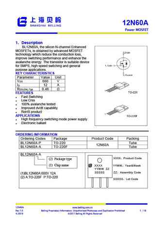
12N60A Power MOSFET 1 Description Step-Down Converter BL12N60A, the silicon N-channel Enhanced , MOSFETs, is obtained by advanced MOSFET technology which reduce the conduction loss, improve switching performance and enhance the avalanche energy. The transistor is suitable device for SMPS, high speed switching and general purpose applications. KEY CHARACTERISTICS Par
blv2n60.pdf
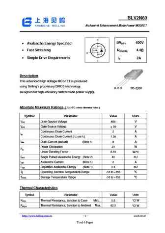
BLV2N60 N-channel Enhancement Mode Power MOSFET 600V DSS Avalanche Energy Specified BV Fast Switching RDS(ON) 4.4 Simple Drive Requirements ID 2A Description This advanced high voltage MOSFET is produced using Belling s proprietary DMOS technology. Designed for high efficiency switch mode power supply. Absolute Maximum Ratings ( TC=25oC unless
bl2n60-p bl2n60-a bl2n60-u bl2n60-d.pdf
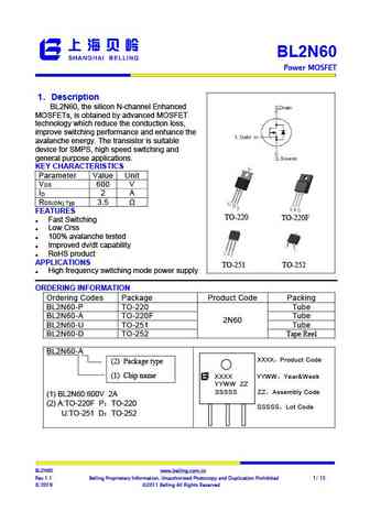
BL2N60 Power MOSFET 1 Description Step-Down Converter BL2N60, the silicon N-channel Enhanced , MOSFETs, is obtained by advanced MOSFET technology which reduce the conduction loss, improve switching performance and enhance the avalanche energy. The transistor is suitable device for SMPS, high speed switching and general purpose applications. KEY CHARACTERISTICS Para
ctm02n60.pdf
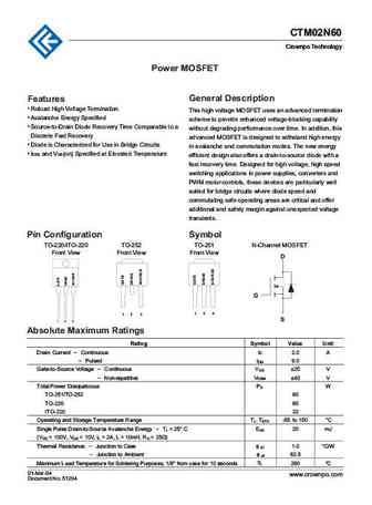
CTM02N60 CTM02N60 Crownpo Technology Crownpo Technology Power MOSFET Features General Description Robust High Voltage Termination This high voltage MOSFET uses an advanced termination Avalanche Energy Specified scheme to provide enhanced voltage-blocking capability Source-to-Drain Diode Recovery Time Comparable to a without degrading performance over time. In addition,
dff2n60.pdf
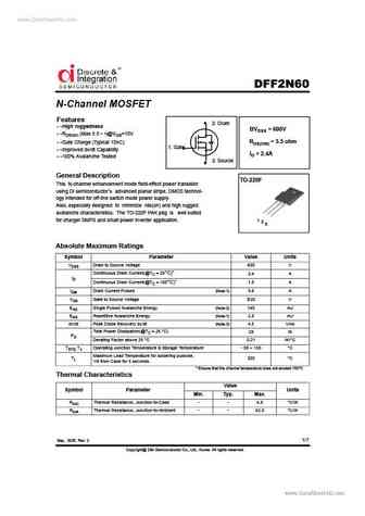
www.DataSheet4U.com DFF2N60 N-Channel MOSFET Features 2. Drain High ruggedness BVDSS = 600V RDS(on) (Max 5.5 )@VGS=10V RDS(ON) = 5.5 ohm Gate Charge (Typical 15nC) 1. Gate Improved dv/dt Capability ID = 2.4A 100% Avalanche Tested 3. Source General Description TO-220F This N-channel enhanceme
fhf2n60e fhp2n60e fhu2n60e fhd2n60e.pdf
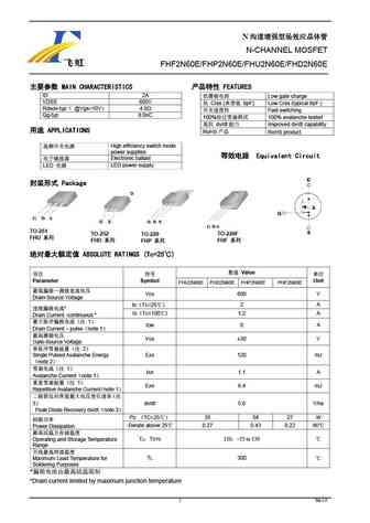
N N-CHANNEL MOSFET FHF2N60E/FHP2N60E/FHU2N60E/FHD2N60E MAIN CHARACTERISTICS FEATURES ID 2A Low gate charge VDSS 600V Crss ( 6pF) Low Crss (typical 6pF ) Rdson-typ @Vgs=10V 4.0 Fast switching Qg-typ 8.0nC 100% 100% avalanche tested dv/
fhf2n60a fhp2n60a fhu2n60a fhd2n60a.pdf
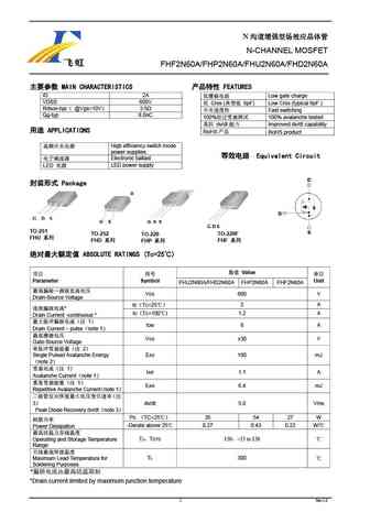
N N-CHANNEL MOSFET FHF2N60A/FHP2N60A/FHU2N60A/FHD2N60A MAIN CHARACTERISTICS FEATURES ID 2A Low gate charge VDSS 600V Crss ( 6pF) Low Crss (typical 6pF ) Rdson-typ @Vgs=10V 3.5 Fast switching Qg-typ 8.0nC 100% 100% avalanche tested dv/
fhp12n60a fhf12n60a.pdf
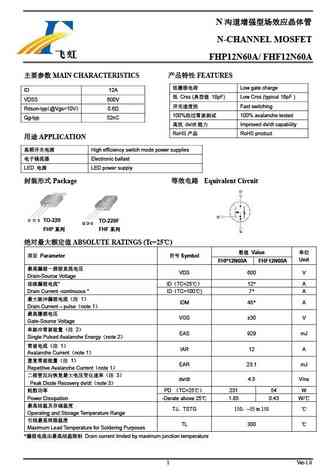
N N-CHANNEL MOSFET FHP12N60A/ FHF12N60A MAIN CHARACTERISTICS FEATURES Low gate charge ID 12A Crss ( 18pF) Low Crss (typical 18pF ) VDSS 600V Fast switching Rdson-typ 0.6 @Vgs=10V 100% 100% avalanche tested Qg-typ 52nC dv/dt Im
cs2n60i.pdf
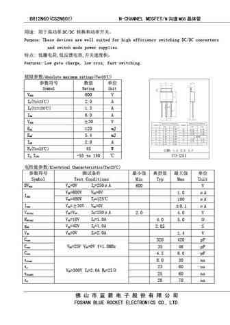
BRI2N60(CS2N60I) N-CHANNEL MOSFET/N MOS DC/DC Purpose These devices are well suited for high efficiency switching DC/DC converters and switch mode power supplies. , , Features Low gate charge, low crss, fast switching. /Absolute maximum ratings(Ta=25
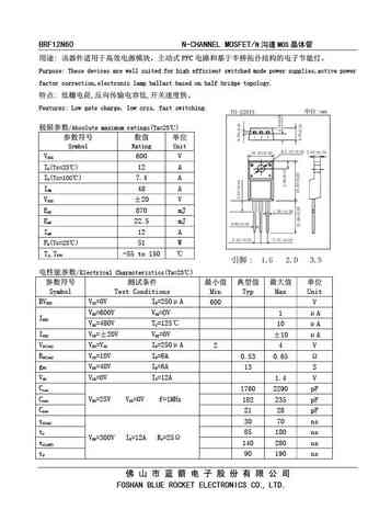
ssf2n60d1.pdf
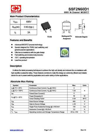
SSF2N60D1 600V N-Channel MOSFET Main Product Characteristics VDSS 600V RDS(on) 3.9 (typ.) ID 2A TO-252 Marking and Pin S c he mati c Diag r a m Assignment Features and Benefits Advanced MOSFET process technology Special designed for PWM, load switching and general purpose applications Ultra low on-resistance with low gate charge Fast switching and re
hy2n60d.pdf
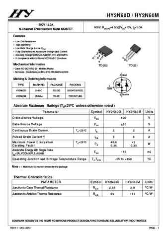
HY2N60D / HY2N60M 600V / 2.0A 600V, RDS(ON)=4.6 @VGS=10V, ID=1.0A N-Channel Enhancement Mode MOSFET Features Low ON Resistance Fast Switching Low Gate Charge & Low CRSS Fully Characterized Avalanche Voltage and Current Specially Desigened for AC Adapter, PFC and SMPS 2 1 1 D G 2 In compliance with EU RoHs 2002/95/EC Directives G 3 DS3 S Mechanical Info
hy2n60t.pdf
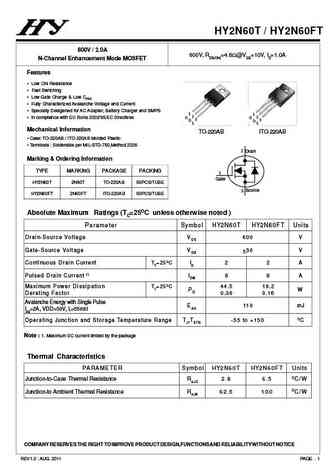
HY2N60T / HY2N60FT 600V / 2.0A 600V, RDS(ON)=4.6 @VGS=10V, ID=1.0A N-Channel Enhancement Mode MOSFET Features Low ON Resistance Fast Switching Low Gate Charge & Low CRSS Fully Characterized Avalanche Voltage and Current Specially Desigened for AC Adapter, Battery Charger and SMPS 1 1 2 2 In compliance with EU RoHs 2002/95/EC Directives G G 3 3 D D S
jfpc12n60c jffm12n60c.pdf
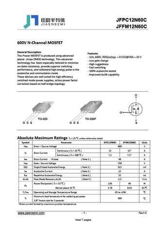
JFPC12N60C JFFM12N60C 600V N-Channel MOSFET General Description Features This Power MOSFET is produced using advanced - 12A, 600V, RDS(on)typ. = 0.52 @VGS = 10 V planar stripe DMOS technology. This advanced - Low gate charge technology has been especially tailored to minimize - High ruggedness on-state resistance, provide superior switching - Fast switching performan
kia2n60h.pdf
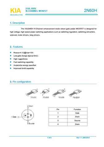
2.0A, 600V N-CHANNELMOSFET 2N60H KIA KIA KIA SEMICONDUCTORS SEMICONDUCTORS SEMICONDUCTORS 1.Description The KIA2N60HN-Channel enhancement mode silicon gate power MOSFET is designed for high voltage, high speed power switching applications such as switchingregulators, switchingconverters, solenoid, motor drivers, relay drivers. 2. Features R =4.1 @V =10V. DS(ON) GS Lowgate cha
kia12n60h.pdf
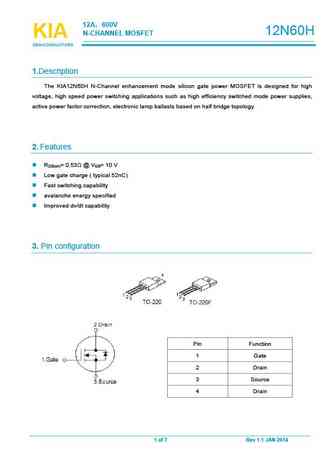
12A 600V 12N60H N-CHANNELMOSFET KIA KIA KIA SEMICONDUCTORS SEMICONDUCTORS SEMICONDUCTORS 1.Description The KIA12N60H N-Channel enhancement mode silicon gate power MOSFET is designed for high voltage, high speed power switching applications such as high efficiency switched mode power supplies, active power factor correction, electronic lamp ballasts based on half bridge topology.
cs12n60.pdf
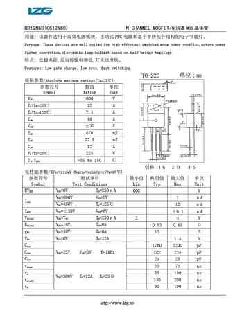
BR12N60(CS12N60) N-CHANNEL MOSFET/N MOS PFC Purpose These devices are well suited for high efficient switched mode power supplies,active power factor correction,electronic lamp ballast based on half bridge topology. , ,
slp12n60c slf12n60c.pdf
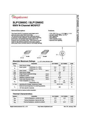
SLP12N60C / SLF12N60C 600V N-Channel MOSFET General Description Features This Power MOSFET is produced using Maple semi s - 12.0A, 600V, RDS(on)typ = 0.51 @VGS = 10 V advanced planar stripe DMOS technology. - Low gate charge ( typical 44.7nC) This advanced technology has been especially tailored - High ruggedness to minimize on-state resistance, provide superior switching - Fast switch
ptp12n60 pta12n60.pdf
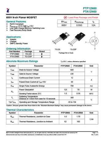
PTP12N60 PTA12N60 600V N-ch Planar MOSFET General Features BVDSS RDS(ON),typ. ID RoHS Compliant 600V 0.55 12A RDS(ON),typ.=0.55 @VGS=10V Low Gate Charge Minimize Switching Loss Fast Recovery Body Diode Applications Adaptor Charger G D S G D SMPS Standby Power S Ordering Information TO-220 TO-220F Part Number Package Brand
pta22n60.pdf
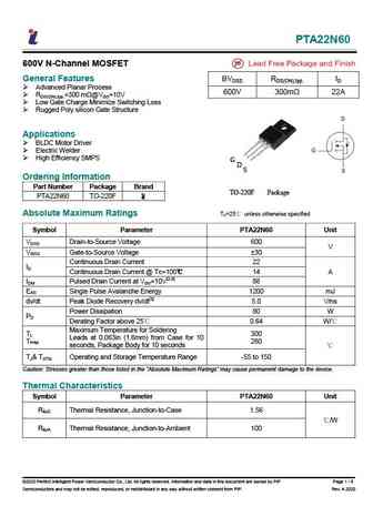
PTA22N60 600V N-Channel MOSFET General Features BVDSS RDS(ON),typ. ID Advanced Planar Process 600V 300m 22A RDS(ON),typ.=300 m @VGS=10V Low Gate Charge Minimize Switching Loss Rugged Poly silicon Gate Structure Applications BLDC Motor Driver Electric Welder High Efficiency SMPS G D S Ordering Information Part Number Package Brand TO-220F Package P
sw2n60b.pdf
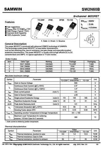
SAMWIN SW2N60B N-channel MOSFET TO-220F IPAK DPAK TO-126 BVDSS 600V Features ID 2.0A High ruggedness RDS(ON) 4.5ohm RDS(ON) (Max 4.5 )@VGS=10V Gate Charge (Typical 7.5nC) 2 Improved dv/dt Capability 1 2 1 2 1 100% Avalanche Tested 3 1 3 2 2 3 3 1 1. Gate 2. Drain 3. Source General Description 3 This power MOSFET is
swf12n60d.pdf
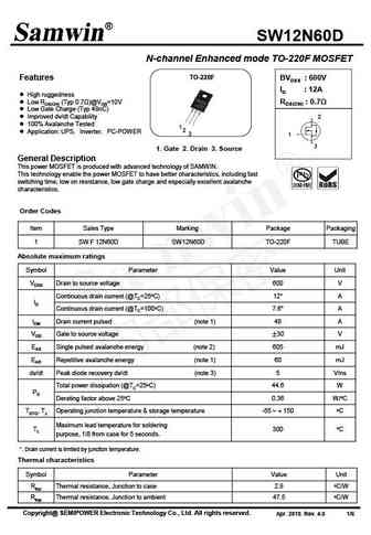
SW12N60D N-channel Enhanced mode TO-220F MOSFET TO-220F Features BVDSS 600V ID 12A High ruggedness Low RDS(ON) (Typ 0.7 )@VGS=10V RDS(ON) 0.7 Low Gate Charge (Typ 48nC) Improved dv/dt Capability 2 100% Avalanche Tested 1 2 Application UPS Inverter PC-POWER 3 1 3 1. Gate 2. Drain 3. Source General Description This power
swd2n60dc swi2n60dc.pdf
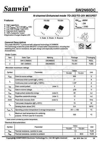
SW2N60DC N-channel Enhanced mode TO-252/TO-251 MOSFET BVDSS 600V Features TO-252 TO-251 ID 2A High ruggedness RDS(ON) 3.9 Low RDS(ON) (Typ 3.9 )@VGS=10V Low Gate Charge (Typ9.5nC) Improved dv/dt Capability 1 100% Avalanche Tested 2 2 1 3 2 Application Charger,Adaptor,LED 3 1 1. Gate 2. Drain 3. Source 3 General Descripti
swf2n60db.pdf
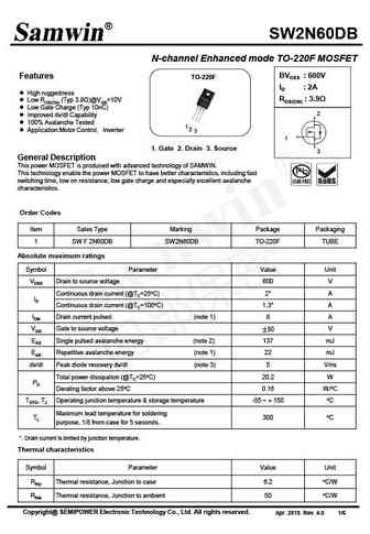
SW2N60DB N-channel Enhanced mode TO-220F MOSFET BVDSS 600V Features TO-220F ID 2A High ruggedness RDS(ON) 3.9 Low RDS(ON) (Typ 3.9 )@VGS=10V Low Gate Charge (Typ 10nC) 2 Improved dv/dt Capability 100% Avalanche Tested 1 2 Application Motor Control Inverter 3 1 1. Gate 2. Drain 3. Source 3 General Description This power
sw2n60a1.pdf
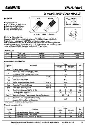
SAMWIN SW2N60A1 SW2N60A1 N-channel IPAK/TO-220F MOSFET TO-251 TO-220F BVDSS 600V Features ID 2.0A High ruggedness RDS(ON) 5.0ohm RDS(ON) (Max 5.0 )@VGS=10V Gate Charge (Typical 10nC) Improved dv/dt Capability 1 1 2 100% Avalanche Tested 2 2 3 3 1. Gate 2. Drain 3. Source 1 General Description 3 This power MOSFET is produced w
sw2n60d.pdf
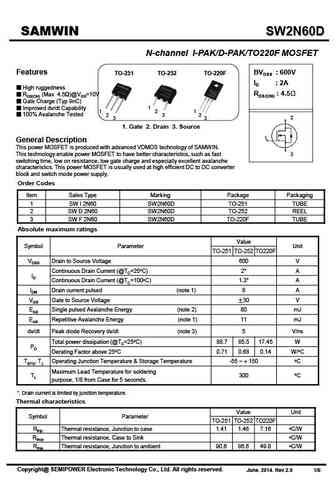
SAMWIN SW2N60D N-channel I-PAK/D-PAK/TO220F MOSFET BVDSS 600V Features TO-252 TO-251 TO-220F ID 2A High ruggedness RDS(ON) 4.5 RDS(ON) (Max 4.5 )@VGS=10V Gate Charge (Typ 9nC) Improved dv/dt Capability 1 1 2 1 100% Avalanche Tested 2 3 2 2 3 3 1. Gate 2. Drain 3. Source 1 General Description This power MOSFET is produced with ad
sw2n60.pdf
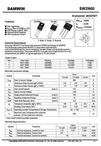
SW2N60 SW2N60 SAMWIN N-channel MOSFET BVDSS 600V TO-220F TO-220 TO-251 Features ID 2.0A High ruggedness RDS(ON) 5.0ohm RDS(ON) (Max 5.0 )@VGS=10V Gate Charge (Typical 15nC) Improved dv/dt Capability 2 100% Avalanche Tested 1 1 2 1 2 3 2 3 3 1 1. Gate 2. Drain 3. Source General Description 3 This power MOSFET is produced wit
srm2n60.pdf
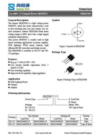
Datasheet 2A, 600V, N-Channel Power MOSFET SRM2N60 General Description Symbol The Sanrise SRM2N60 is a high voltage power MOSFET, which has better characteristics, such as fast switching time, low gate charge, low on- state resistance. Sanrise SRM2N60 break down voltage rating is 600V and it has a high rugged avalanche characteristics. This power MOSFET is usually used at high
hfs12n60s.pdf
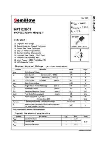
Nov 2007 BVDSS = 600 V RDS(on) typ = 0.53 HFS12N60S ID = 12 A 600V N-Channel MOSFET TO-220F FEATURES 1 Originative New Design 2 3 Superior Avalanche Rugged Technology 1.Gate 2. Drain 3. Source Robust Gate Oxide Technology Very Low Intrinsic Capacitances Excellent Switching Characteristics Unrivalled Gate Charge 38 nC (Typ.) Unrivalled Gate Charge 38 nC (Typ ) E
hfs2n60.pdf
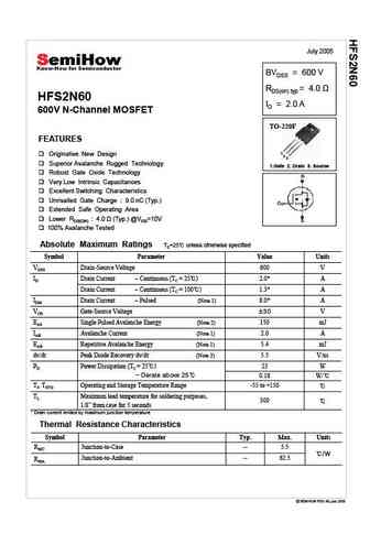
July 2005 BVDSS = 600 V RDS(on) typ HFS2N60 ID = 2.0 A 600V N-Channel MOSFET TO-220F FEATURES 1 Originative New Design 2 3 Superior Avalanche Rugged Technology 1.Gate 2. Drain 3. Source Robust Gate Oxide Technology Very Low Intrinsic Capacitances Excellent Switching Characteristics Unrivalled Gate Charge 9.0 nC (Typ.) Extended Safe Operating Area Lower RDS
hfp2n60f hfs2n60f.pdf
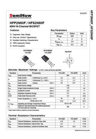
Oct 2016 HFP2N60F / HFS2N60F 600V N-Channel MOSFET Features Key Parameters Parameter Value Unit Originative New Design BVDSS 600 V Very Low Intrinsic Capacitances ID 2A Excellent Switching Characteristics RDS(on), Typ 3.6 100% Avalanche Tested Qg, Typ 6.5 nC RoHS Compliant HFP2N60F HFS2N60F Symbol TO-220 TO-220F S S D D G G Absolute Maximum Ratings TC=25 unles
hfp2n60u.pdf
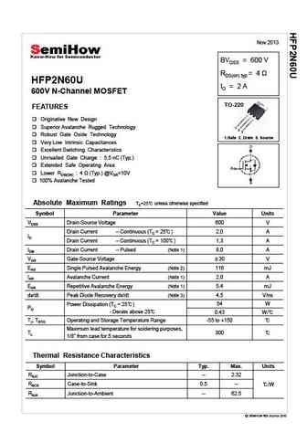
Nov 2013 BVDSS = 600 V RDS(on) typ = HFP2N60U ID = 2 A 600V N-Channel MOSFET TO-220 FEATURES Originative New Design Superior Avalanche Rugged Technology 1 2 3 Robust Gate Oxide Technology 1.Gate 2. Drain 3. Source Very Low Intrinsic Capacitances Excellent Switching Characteristics Unrivalled Gate Charge 5.5 nC (Typ.) Extended Safe Operating Area Lower R
hfd2n60u hfu2n60u.pdf

June 2015 BVDSS = 600 V RDS(on) typ = 4 HFD2N60U / HFU2N60U ID = 1.8 A 600V N-Channel MOSFET D-PAK I-PAK FEATURES 2 1 Originative New Design 1 3 2 3 Superior Avalanche Rugged Technology HFD2N60U HFU2N60U Robust Gate Oxide Technology 1.Gate 2. Drain 3. Source Very Low Intrinsic Capacitances Excellent Switching Characteristics Unrivalled Gate Charge 5.5 nC (T
hfs2n60s.pdf
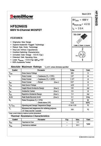
March 2014 BVDSS = 600 V RDS(on) typ HFS2N60S ID = 2.0 A 600V N-Channel MOSFET TO-220F FEATURES 1 Originative New Design 2 3 Superior Avalanche Rugged Technology 1.Gate 2. Drain 3. Source Robust Gate Oxide Technology Very Low Intrinsic Capacitances Excellent Switching Characteristics Unrivalled Gate Charge 6.0 nC (Typ.) Extended Safe Operating Area
hfc2n60u.pdf
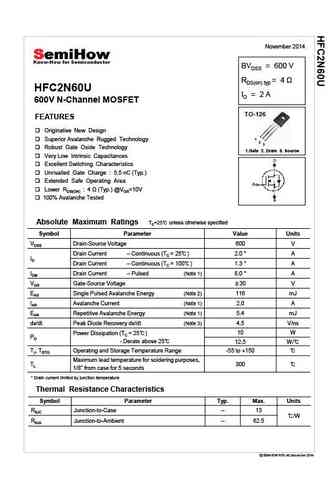
November 2014 BVDSS = 600 V RDS(on) typ = HFC2N60U ID = 2 A 600V N-Channel MOSFET TO-126 FEATURES Originative New Design 1 Superior Avalanche Rugged Technology 2 3 Robust Gate Oxide Technology 1.Gate 2. Drain 3. Source Very Low Intrinsic Capacitances Excellent Switching Characteristics Unrivalled Gate Charge 5.5 nC (Typ.) Extended Safe Operating Area L
hfd2n60u.pdf
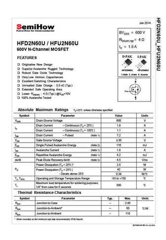
Jan 2014 BVDSS = 600 V RDS(on) typ = 4 HFD2N60U / HFU2N60U ID = 1.8 A 600V N-Channel MOSFET D-PAK I-PAK FEATURES 2 1 Originative New Design 1 3 2 3 Superior Avalanche Rugged Technology HFD2N60U HFU2N60U Robust Gate Oxide Technology 1.Gate 2. Drain 3. Source Very Low Intrinsic Capacitances Excellent Switching Characteristics Unrivalled Gate Charge 5.5 nC (Ty
hfp12n60u.pdf
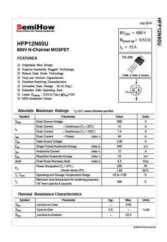
July 2014 BVDSS = 600 V RDS(on) typ = 0.53 HFP12N60U ID = 12 A 600V N-Channel MOSFET TO-220 FEATURES Originative New Design Superior Avalanche Rugged Technology 1 2 3 Robust Gate Oxide Technology 1.Gate 2. Drain 3. Source Very Low Intrinsic Capacitances Excellent Switching Characteristics Unrivalled Gate Charge 42 nC (Typ.) Extended Safe Operating Area Lo
hfp2n60s.pdf
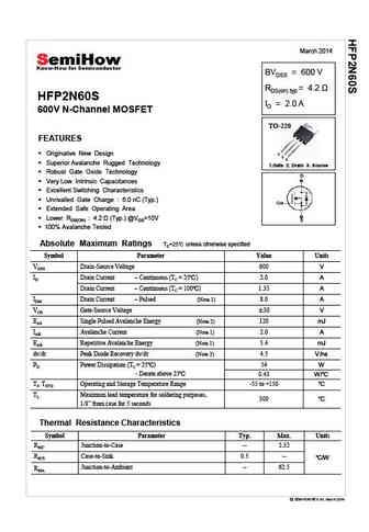
March 2014 BVDSS = 600 V RDS(on) typ HFP2N60S ID = 2.0 A 600V N-Channel MOSFET TO-220 FEATURES Originative New Design 1 2 3 Superior Avalanche Rugged Technology 1.Gate 2. Drain 3. Source Robust Gate Oxide Technology Very Low Intrinsic Capacitances Excellent Switching Characteristics Unrivalled Gate Charge 6.0 nC (Typ.) Extended Safe Operating Area L
hfp12n60s.pdf
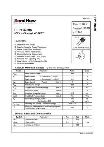
Nov 2007 BVDSS = 600 V RDS(on) typ = 0.53 HFP12N60S ID = 12 A 600V N-Channel MOSFET TO-220 FEATURES Originative New Design 1 2 3 Superior Avalanche Rugged Technology 1.Gate 2. Drain 3. Source Robust Gate Oxide Technology Very Low Intrinsic Capacitances Excellent Switching Characteristics Unrivalled Gate Charge 38 nC (Typ.) Unrivalled Gate Charge 38 nC (Typ ) Ext
hfd2n60s.pdf

March 2014 BVDSS = 600 V RDS(on) typ HFD2N60S / HFU2N60S ID = 1.9 A 600V N-Channel MOSFET D-PAK I-PAK 2 FEATURES 1 1 3 2 3 Originative New Design HFD2N60S HFU2N60S Superior Avalanche Rugged Technology 1.Gate 2. Drain 3. Source Robust Gate Oxide Technology Very Low Intrinsic Capacitances Excellent Switching Characteristics Unrivalled Gate Charge 6.0 nC
hfs12n60u.pdf
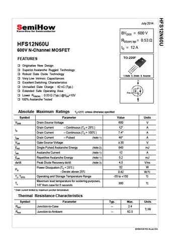
July 2014 BVDSS = 600 V RDS(on) typ = 0.53 HFS12N60U ID = 12 A 600V N-Channel MOSFET TO-220F FEATURES Originative New Design Superior Avalanche Rugged Technology 1 2 3 Robust Gate Oxide Technology 1.Gate 2. Drain 3. Source Very Low Intrinsic Capacitances Excellent Switching Characteristics Unrivalled Gate Charge 42 nC (Typ.) Extended Safe Operating Area Lo
hfs2n60fs.pdf
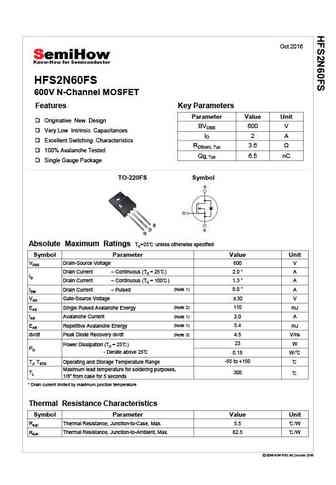
Oct 2016 HFS2N60FS 600V N-Channel MOSFET Features Key Parameters Parameter Value Unit Originative New Design BVDSS 600 V Very Low Intrinsic Capacitances ID 2A Excellent Switching Characteristics RDS(on), Typ 3.6 100% Avalanche Tested Qg, Typ 6.5 nC Single Gauge Package TO-220FS Symbol S D G Absolute Maximum Ratings TC=25 unless otherwise specified Symbol Paramete
hfs2n60u.pdf
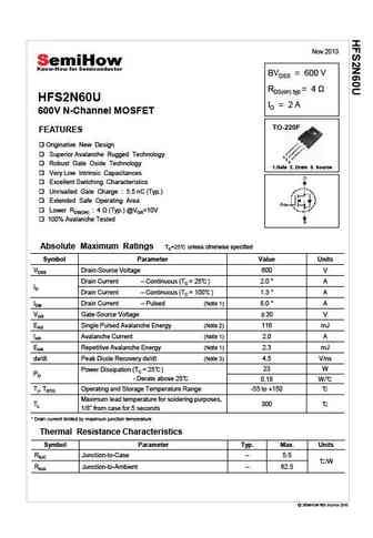
Nov 2013 BVDSS = 600 V RDS(on) typ HFS2N60U ID = 2 A 600V N-Channel MOSFET TO-220F FEATURES Originative New Design Superior Avalanche Rugged Technology 1 2 3 Robust Gate Oxide Technology 1.Gate 2. Drain 3. Source Very Low Intrinsic Capacitances Excellent Switching Characteristics Unrivalled Gate Charge 5.5 nC (Typ.) Extended Safe Operating Area Lower
hfd2n60.pdf
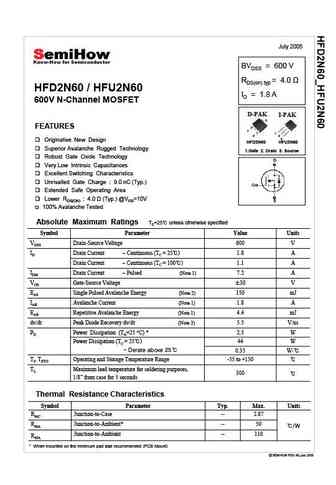
July 2005 BVDSS = 600 V RDS(on) typ HFD2N60 / HFU2N60 ID = 1.8 A 600V N-Channel MOSFET D-PAK I-PAK 2 FEATURES 1 1 3 2 3 Originative New Design HFD2N60 HFU2N60 Superior Avalanche Rugged Technology 1.Gate 2. Drain 3. Source Robust Gate Oxide Technology Very Low Intrinsic Capacitances Excellent Switching Characteristics Unrivalled Gate Charge 9.0 nC (Typ
hfu2n60f hfd2n60f.pdf
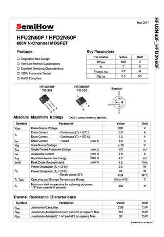
May 2017 HFU2N60F / HFD2N60F 600V N-Channel MOSFET Features Key Parameters Parameter Value Unit Originative New Design BVDSS 600 V Very Low Intrinsic Capacitances ID 2 A Excellent Switching Characteristics RDS(on), Typ 3.6 100% Avalanche Tested Qg, Typ 6.5 nC RoHS Compliant HFU2N60F HFD2N60F Symbol TO-251 TO-252 D S S G D G Ab
hfw12n60s.pdf
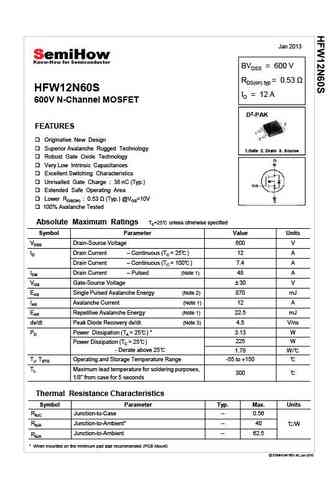
Jan 2013 BVDSS = 600 V RDS(on) typ = 0.53 HFW12N60S ID = 12 A 600V N-Channel MOSFET D2-PAK FEATURES Originative New Design Superior Avalanche Rugged Technology 1.Gate 2. Drain 3. Source Robust Gate Oxide Technology Very Low Intrinsic Capacitances Excellent Switching Characteristics Unrivalled Gate Charge 38 nC (Typ.) Extended Safe Operating Area Lower RDS(ON
hfd2n60s hfu2n60s.pdf
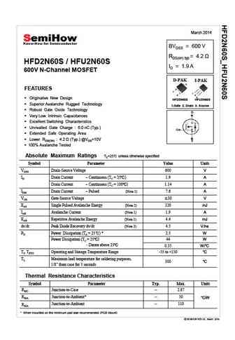
March 2014 BVDSS = 600 V RDS(on) typ HFD2N60S / HFU2N60S ID = 1.9 A 600V N-Channel MOSFET D-PAK I-PAK 2 FEATURES 1 1 3 2 3 Originative New Design HFD2N60S HFU2N60S Superior Avalanche Rugged Technology 1.Gate 2. Drain 3. Source Robust Gate Oxide Technology Very Low Intrinsic Capacitances Excellent Switching Characteristics Unrivalled Gate Charge 6.0 nC
sff12n60.pdf
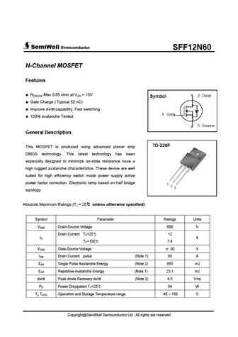
SemiWell Semiconductor SFF12N60 N-Channel MOSFET Features RDS(ON) Max 0.65 ohm at VGS = 10V Gate Charge ( Typical 52 nC) Improve dv/dt capability, Fast switching 100% avalanche Tested General Description This MOSFET is produced using advanced planar strip DMOS technology. This latest technology has been especially designed to minimize on-state resistance h
sff2n60-kr.pdf
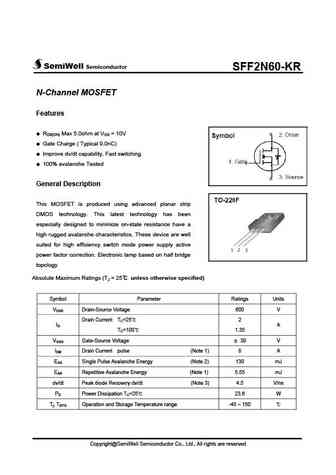
SemiWell Semiconductor SFF2N60-KR N-Channel MOSFET Features RDS(ON) Max 5.0ohm at VGS = 10V Gate Charge ( Typical 9.0nC) Improve dv/dt capability, Fast switching 100% avalanche Tested General Description This MOSFET is produced using advanced planar strip DMOS technology. This latest technology has been especially designed to minimize on-state resistance ha
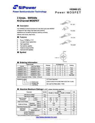
msk2n60f msk2n60t.pdf
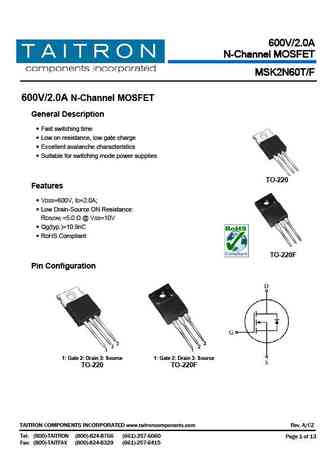
600V/2.0A N-Channel MOSFET MSK2N60T/F 600V/2.0A N-Channel MOSFET General Description Fast switching time Low on resistance, low gate charge Excellent avalanche characteristics Suitable for switching mode power supplies TO-220 Features VDSS=600V, ID=2.0A; Low Drain-Source ON Resistance RDS(ON) =5.0 @ VGS=10V Qg(typ.)=10.9nC RoHS C
msu2n60.pdf
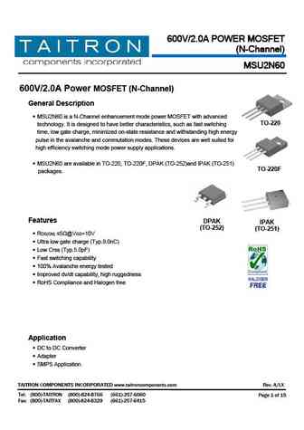
600V/2.0A POWER MOSFET (N-Channel) MSU2N60 600V/2.0A Power MOSFET (N-Channel) General Description MSU2N60 is a N-Channel enhancement mode power MOSFET with advanced TO-220 technology. It is designed to have better characteristics, such as fast switching time, low gate charge, minimized on-state resistance and withstanding high energy pulse in the avalanche and commutati
msu12n60f msu12n60t.pdf
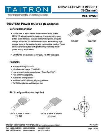
600V/12A POWER MOSFET (N-Channel) MSU12N60 600V/12A Power MOSFET (N-Channel) General Description MSU12N60 is a N-Channel enhancement mode power MOSFET with advanced technology. It is designed to have Better characteristics, such as fast switching time, low gate TO-220 TO-220F charge, minimized on-state resistance and withstanding high energy pulse in the avalanche and
tmp12n60a tmpf12n60a.pdf
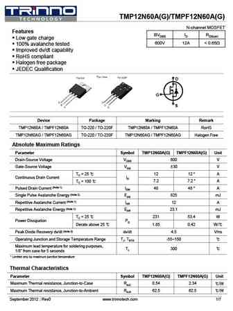
TMP12N60A(G)/TMPF12N60A(G) N-channel MOSFET Features BVDSS ID RDS(on) Low gate charge 600V 12A
tmt2n60zg.pdf
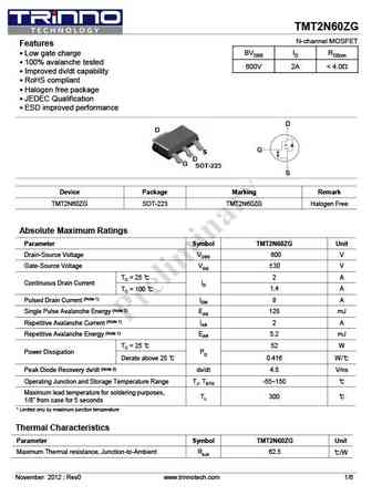
TMT2N60ZG N-channel MOSFET Features Low gate charge BVDSS ID RDS(on 100% avalanche tested 600V 2A
tmp2n60z tmpf2n60z.pdf
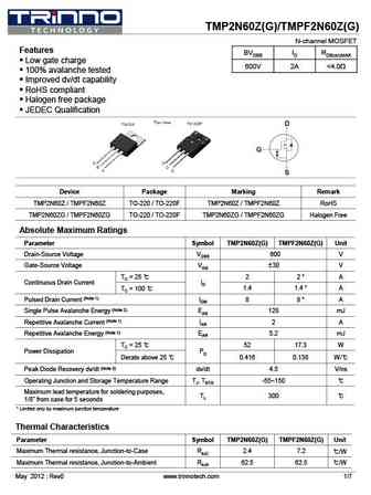
TMP2N60Z(G)/TMPF2N60Z(G) N-channel MOSFET Features BVDSS ID RDS(on)MAX Low gate charge 600V 2A
tmd2n60z tmu2n60z.pdf
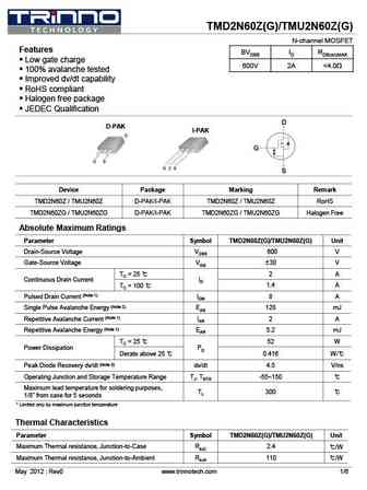
TMD2N60Z(G)/TMU2N60Z(G) N-channel MOSFET Features BVDSS ID RDS(on)MAX Low gate charge 600V 2A
tmp2n60az tmpf2n60az.pdf
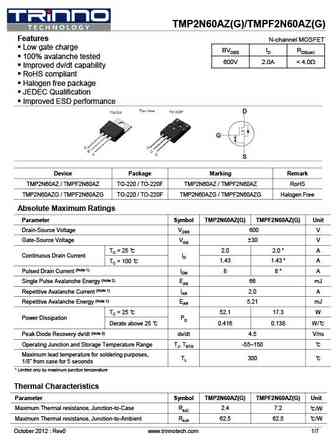
TMP2N60AZ(G)/TMPF2N60AZ(G) Features N-channel MOSFET Low gate charge BVDSS ID RDS(on) 100% avalanche tested 600V 2.0A
tmd2n60az tmu2n60az.pdf
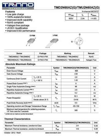
TMD2N60AZ(G)/TMU2N60AZ(G) N-channel MOSFET Features Low gate charge BVDSS ID RDS(on) 100% avalanche tested 600V 2.0A
tmp12n60 tmpf12n60.pdf
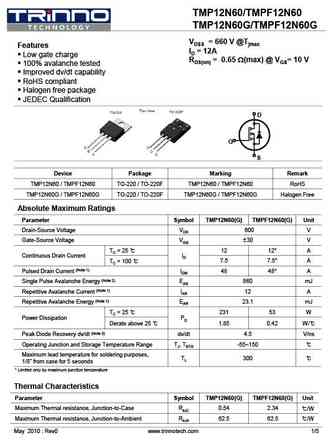
TMP12N60/TMPF12N60 TMP12N60G/TMPF12N60G VDSS = 660 V @Tjmax Features ID = 12A Low gate charge RDS(on) = 0.65 W(max) @ VGS= 10 V 100% avalanche tested Improved dv/dt capability RoHS compliant Halogen free package JEDEC Qualification D G S Device Package Marking Remark TMP12N60 / TMPF12N60 TO-220 / TO-220F TMP12N60 / TMPF12N60 RoHS TMP12N60G / TMPF12N60G
tsp12n60m tsf12n60m.pdf
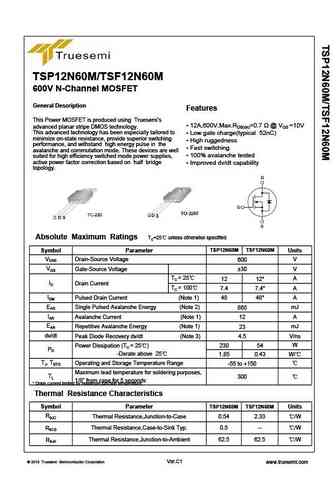
TSP12N60M/TSF12N60M 600V N-Channel MOSFET General Description Features This Power MOSFET is produced using Truesemi s 12A,600V,Max.RDS(on)=0.7 @ VGS =10V advanced planar stripe DMOS technology. This advanced technology has been especially tailored to Low gate charge(typical 52nC) minimize on-state resistance, provide superior switching High ruggedness performance, an
cs12n60fa9r.pdf
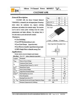
Silicon N-Channel Power MOSFET R CS12N60F A9R General Description VDSS 600 V CS12N60F A9R, the silicon N-channel Enhanced ID 12 A PD(TC=25 ) 42 W VDMOSFETs, is obtained by the self-aligned planar Technology RDS(ON)Typ 0.57 which reduce the conduction loss, improve switching performance and enhance the avalanche energy. The transistor can be used in various p
cs2n60fa9h.pdf
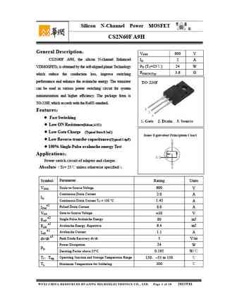
Silicon N-Channel Power MOSFET R CS2N60F A9H General Description VDSS 600 V CS2N60F A9H, the silicon N-channel Enhanced ID 2 A PD (TC=25 ) 24 W VDMOSFETs, is obtained by the self-aligned planar Technology RDS(ON)Typ 3.6 which reduce the conduction loss, improve switching performance and enhance the avalanche energy. The transistor can be used in various pow
cs12n60a8hd.pdf
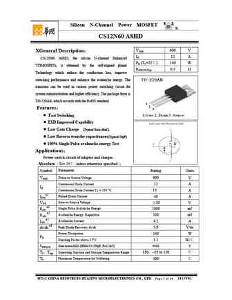
Silicon N-Channel Power MOSFET R CS12N60 A8HD VDSS 600 V XGeneral Description ID 12 A CS12N60 A8HD, the silicon N-channel Enhanced PD (TC=25 ) 140 W VDMOSFETs, is obtained by the self-aligned planar RDS(ON)Typ 0.5 Technology which reduce the conduction loss, improve switching performance and enhance the avalanche energy. The transistor can be used in various
cs2n60a7h.pdf

Silicon N-Channel Power MOSFET R CS2N60 A7H General Description VDSS 600 V CS2N60 A7H, the silicon N-channel Enhanced ID 2 A PD (TC=25 ) 24 W VDMOSFETs, is obtained by the self-aligned planar Technology RDS(ON)Typ 3.6 which reduce the conduction loss, improve switching performance and enhance the avalanche energy. The transistor can be used in various power
cs12n60fa9h.pdf

Silicon N-Channel Power MOSFET R CS12N60F A9H VDSS 600 V General Description ID 12 A CS12N60F A9H, the silicon N-channel Enhanced PD (TC=25 ) 55 W VDMOSFETs, is obtained by the self-aligned planar RDS(ON)Typ 0.5 Technology which reduce the conduction loss, improve switching performance and enhance the avalanche energy. The transistor can be used in various
cs2n60a3h.pdf
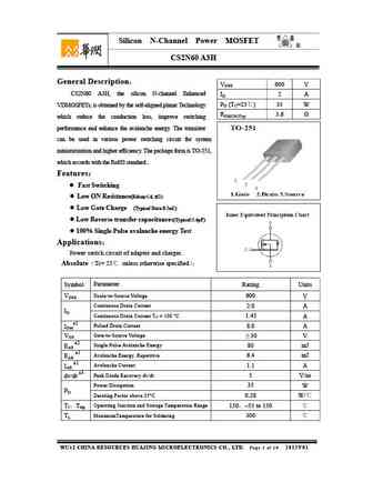
Silicon N-Channel Power MOSFET R CS2N60 A3H General Description VDSS 600 V CS2N60 A3H, the silicon N-channel Enhanced ID 2 A PD (TC=25 ) 35 W VDMOSFETs, is obtained by the self-aligned planar Technology RDS(ON)Typ 3.6 which reduce the conduction loss, improve switching performance and enhance the avalanche energy. The transistor can be used in various power
cs2n60a4t.pdf
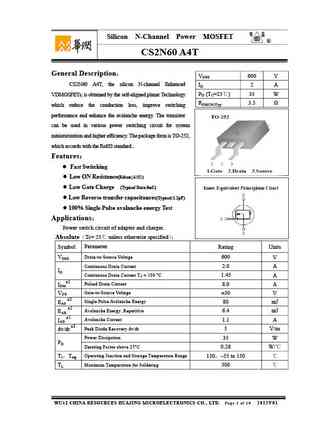
Silicon N-Channel Power MOSFET R CS2N60 A4T General Description VDSS 600 V CS2N60 A4T, the silicon N-channel Enhanced ID 2 A PD (TC=25 ) 35 W VDMOSFETs, is obtained by the self-aligned planar Technology RDS(ON)Typ 3.5 which reduce the conduction loss, improve switching performance and enhance the avalanche energy. The transistor can be used in various power
cs12n60fa9hd.pdf
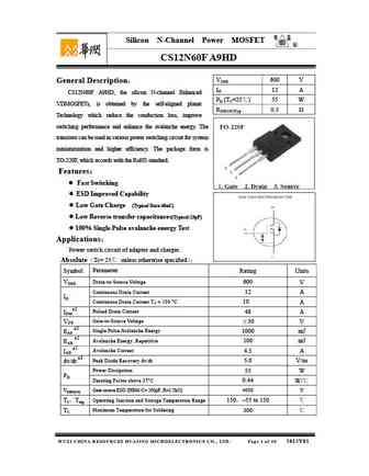
Silicon N-Channel Power MOSFET R CS12N60F A9HD VDSS 600 V General Description ID 12 A CS12N60F A9HD, the silicon N-channel Enhanced PD (TC=25 ) 55 W VDMOSFETs, is obtained by the self-aligned planar RDS(ON)Typ 0.5 Technology which reduce the conduction loss, improve switching performance and enhance the avalanche energy. The transistor can be used in vario
cs2n60a4h.pdf
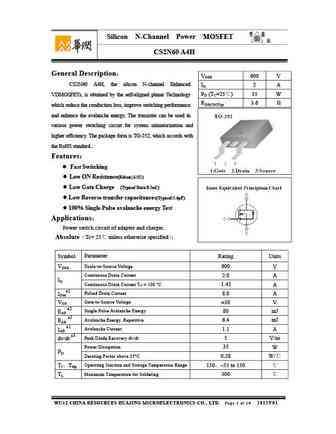
Silicon N-Channel Power MOSFET R CS2N60 A4H General Description VDSS 600 V CS2N60 A4H, the silicon N-channel Enhanced ID 2 A PD (TC=25 ) 35 W VDMOSFETs, is obtained by the self-aligned planar Technology RDS(ON)Typ 3.6 which reduce the conduction loss, improve switching performance and enhance the avalanche energy. The transistor can be used in various power
cs12n60a8h.pdf

Silicon N-Channel Power MOSFET R CS12N60 A8H VDSS 600 V General Description ID 12 A CS12N60 A8H, the silicon N-channel Enhanced PD (TC=25 ) 140 W VDMOSFETs, is obtained by the self-aligned planar RDS(ON)Typ 0.5 Technology which reduce the conduction loss, improve switching performance and enhance the avalanche energy. The transistor can be used in various po
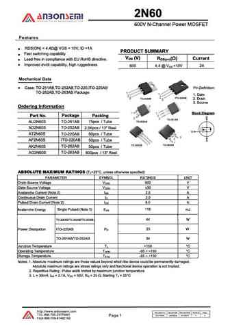
csfr12n60f.pdf
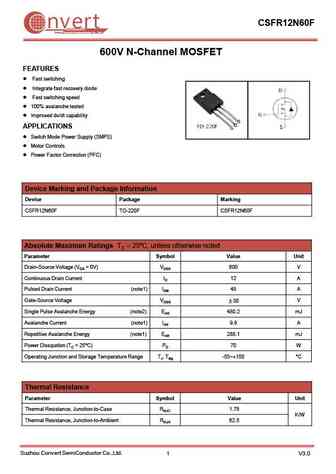
CSFR12N60F nvert Suzhou Convert Semiconductor Co ., Ltd. 600V N-Channel MOSFET FEATURES Fast switching Integrate fast recovery diode Fast switching speed 100% avalanche tested Improved dv/dt capability APPLICATIONS Switch Mode Power Supply (SMPS) Motor Controls Power Factor Correction (PFC) Device Marking and Package Information Device Package Mark
csfr2n60f csfr2n60p csfr2n60u csfr2n60d.pdf
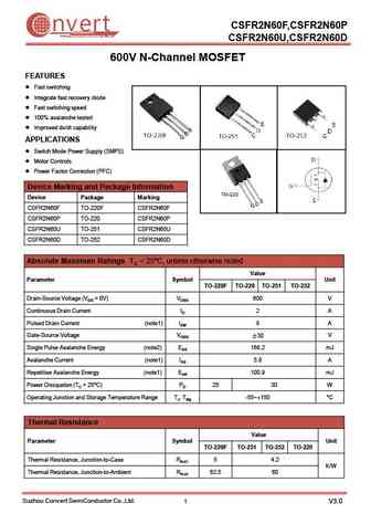
CSFR2N60F,CSFR2N60P nvert Suzhou Convert Semiconductor Co ., Ltd. CSFR2N60U,CSFR2N60D 600V N-Channel MOSFET FEATURES Fast switching Integrate fast recovery diode Fast switching speed 100% avalanche tested Improved dv/dt capability APPLICATIONS Switch Mode Power Supply (SMPS) Motor Controls Power Factor Correction (PFC) Device Marking and Package In
cs2n60f cs2n60p cs2n60u cs2n60d cs2n60c.pdf
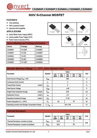
nvert Suzhou Convert Semiconductor Co ., Ltd. CS2N60F,CS2N60P,CS2N60U,CS2N60D,CS2N60C 600V N-Channel MOSFET FEATURES Fast switching 100% avalanche tested Improved dv/dt capability APPLICATIONS Switch Mode Power Supply (SMPS) Uninterruptible Power Supply (UPS) Power Factor Correction (PFC) Device Marking and Package Information Device Package Marking CS2N60F
cs12n60f cs12n60p.pdf
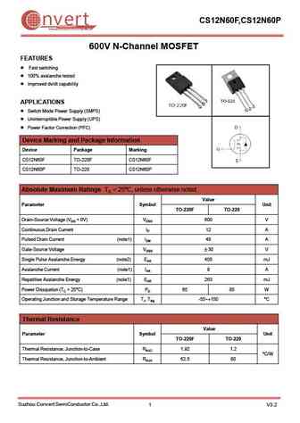
CS12N60F,CS12N60P nvert Suzhou Convert Semiconductor Co ., Ltd. 600V N-Channel MOSFET FEATURES Fast switching 100% avalanche tested Improved dv/dt capability APPLICATIONS Switch Mode Power Supply (SMPS) Uninterruptible Power Supply (UPS) Power Factor Correction (PFC) Device Marking and Package Information Device Package Marking CS12N60F TO-220F CS12N60F CS
fir12n60fg.pdf
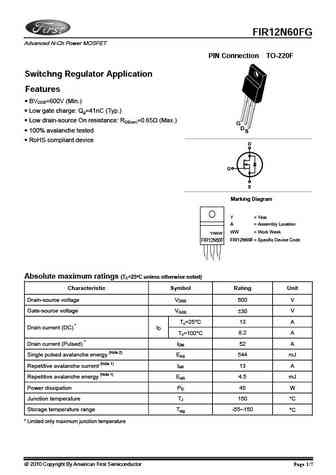
FIR12N60FG Advanced N-Ch Power MOSFET PIN Connection TO-220F Switchng Regulator Application Features BVDDS=600V (Min.) Low gate charge Qg=41nC (Typ.) Low drain-source On resistance RDS(on)=0.65 (Max.) G D S 100% avalanche tested RoHS compliant device D G S Marking Diagram Y = Year A = Assembly Location WW = Work Week YAWW FIR12N60F = Specif
fir2n60alg.pdf
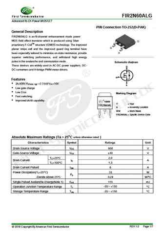
FIR2N60ALG Advanced N-Ch Power MOSFET PIN Connection TO-252(D-PAK) General Description FIR2N60ALG is an N-channel enhancement mode power MOS field effect transistor which is produced using Silan D proprietary F-CellTM structure VDMOS technology. The improved G planar stripe cell and the improved guard ring terminal have been especially tailored to minimize on-state resistance, prov
fir2n60afg.pdf
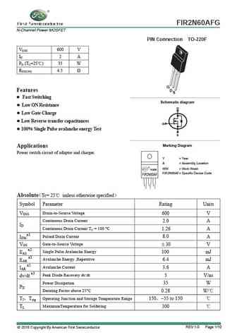
FIR2N60AFG N-Channel Power MOSFET PIN Connection TO-220F VDSS 600 V ID 2 A PD (TC=25 ) 35 W RDS(ON) 4.5 G Features D S Fast Switching g Schematic dia ram Low ON Resistance D Low Gate Charge Low Reverse transfer capacitances G 100% Single Pulse avalanche energy Test S Marking Diagram Applications Power switch circuit of adaptor and charger. Y = Year
smf2n60.pdf
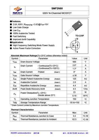
SMF2N60 600V N-Channnel MOSFET Features 2.0A, 600V, R =3.8 @V =10V DS(on)(Typ) GS Low Gate Charge Low C rss 100% Avalanche Tested Fast Switching Improved dv/dt Capability Application High Frequency Switching Mode Power Supply Active Power Factor Correction Absolute Maximum Ratings(Tc=25 C unless otherwise noted) Symbol Parameter Value
smt12n60.pdf
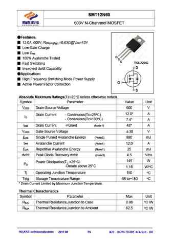
SMT12N60 600V N-Channnel MOSFET Features 12.0A, 600V, R =0.63 @V =10V DS(on)(Typ) GS Low Gate Charge Low C rss 100% Avalanche Tested Fast Switching Improved dv/dt Capability Application High Frequency Switching Mode Power Supply Active Power Factor Correction Absolute Maximum Ratings(Tc=25 C unless otherwise noted) Symbol Parameter Va
smf12n60.pdf

SMF12N60 600V N-Channnel MOSFET Features 12.0A, 600V, R =0.63 @V =10V DS(on)(Typ) GS Low Gate Charge Low C rss 100% Avalanche Tested Fast Switching Improved dv/dt Capability Application High Frequency Switching Mode Power Supply Active Power Factor Correction Absolute Maximum Ratings(Tc=25 C unless otherwise noted) Symbol Parameter Va
hf12n60.pdf
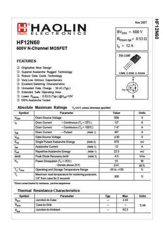
Nov 2007 BVDSS = 600 V RDS(on) typ = 0.53 HF12N60 ID = 12 A 600V N-Channel MOSFET TO-220F FEATURES 1 Originative New Design 2 3 Superior Avalanche Rugged Technology 1.Gate 2. Drain 3. Source Robust Gate Oxide Technology Very Low Intrinsic Capacitances Excellent Switching Characteristics Unrivalled Gate Charge 38 nC (Typ.) Extended Safe Operati
2n5419 2n5420 2n5550 2n5551 2n5830 2n5831 2n5832 2n5998 2n5999 2n6008 2n6009 2n6076 2n6426 2n6427.pdf
jmpf12n60bj.pdf
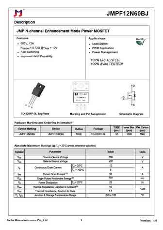
JMPF12N60BJ Description JMP N-channel Enhancement Mode Power MOSFET Features Applications 600V, 12A Load Switch RDS(ON)
jmpc12n60bj.pdf
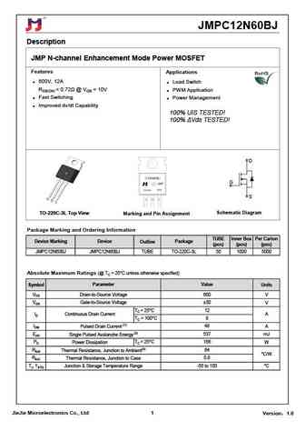
JMPC12N60BJ Description JMP N-channel Enhancement Mode Power MOSFET Features Applications 600V, 12A Load Switch RDS(ON)
lnd12n60 lnc12n60 lne12n60 lnf12n60.pdf
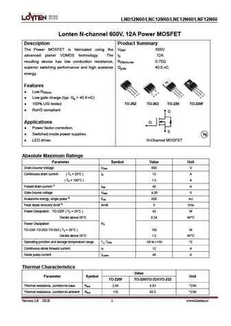
LND12N60/LNC12N60/LNE12N60/LNF12N60 Lonten N-channel 600V, 12A Power MOSFET Description Product Summary The Power MOSFET is fabricated using the VDSS 600V advanced planer VDMOS technology. The ID 12A resulting device has low conduction resistance, RDS(on),max 0.75 superior switching performance and high avalance Qg,typ 40.8 nC energy. Features Low RDS(on) Low gate
lnd2n60 lnc2n60 lng2n60 lnh2n60.pdf

LND2N60/LNC2N60/LNG2N60/LNH2N60 Lonten N-channel 600V, 2A Power MOSFET Description Product Summary The Power MOSFET is fabricated using the V 600V DSS advanced planer VDMOS technology. The I 2A D resulting device has low conduction resistance, R 4.5 DS(on),max superior switching performance and high avalance Q 10.2 nC g,typ energy. Features Low R DS(on) Low gate charge
si12n60.pdf

N-CHANNEL MOSFET SI12N60 ABSOLUTE RATINGS (Tc=25 ) Value Parameter Symbol Unit SSS12N60 VDSS V 600 Drain-Source Voltage ID 12 A Drain Current -continuous T=25 1 IDM 48 A Drain Current - pulse note 1
pjm02n60sa.pdf
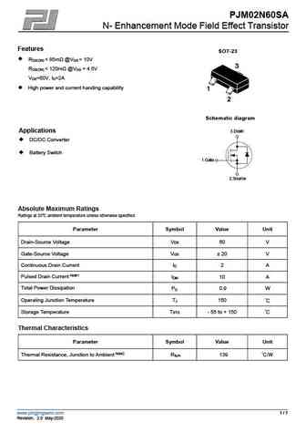
PJM02 60SA N- Enhancement Mode Field Effect Transistor Features SOT-23 R
sss2n60.pdf
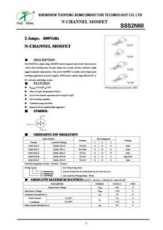
SHENZHEN TUOFENG SEMICONDUCTOR TECHNOLOGY CO. LTD N-CHANNEL MOSFET SSS2N60 2 Amps 600Volts 2 Amps 600Volts 2 Amps 600Volts 2 Amps 600Volts N-CHANNEL MOSFET N-CHANNEL MOSFET N-CHANNEL MOSFET N-CHANNEL MOSFET DESCRIPTION The SSS2N60 is a high voltage MOSFET and is designed to have better characteristics, such as fast switching time, low gate charge, low on-state resistance and
se2n60b.pdf
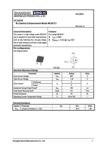
Oct 2014 SE2N60B N-Channel Enhancement-Mode MOSFET Revision A General Description Features This series is a high voltage power MOSFET For a single MOSFET and is designed to have better characteristics, VDS = 600V such as fast switching time, low gate charge, RDS(ON) = 3.4 @ VGS=10V low on-state resistance and have a high rugged avalanche characteristics Pin co
ndf02n60zg.pdf
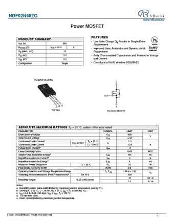
NDF02N60ZG www.VBsemi.tw Power MOSFET FEATURES PRODUCT SUMMARY Low Gate Charge Qg Results in Simple Drive VDS (V) 650 Available Requirement RDS(on) ( )VGS = 10 V 5 RoHS* Improved Gate, Avalanche and Dynamic dV/dt COMPLIANT Qg (Max.) (nC) 11 Ruggedness Qgs (nC) 2.3 Fully Characterized Capacitance and Avalanche Voltage and Current Qgd (nC) 5.2 Compliant to RoHS
fqd2n60c.pdf
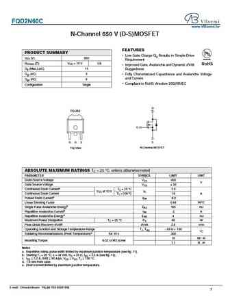
FQD2N60C www.VBsemi.tw N-Channel 650 V (D-S) MOSFET FEATURES PRODUCT SUMMARY Low Gate Charge Qg Results in Simple Drive VDS (V) 650 Available Requirement RDS(on) ( )VGS = 10 V 3.8 RoHS Improved Gate, Avalanche and Dynamic dV/dt Qg (Max.) (nC) 15 Ruggedness Qgs (nC) 3 Fully Characterized Capacitance and Avalanche Voltage and Current Qgd (nC) 6 Compliant to RoHS
vbze2n60.pdf
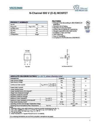
VBZE2N60 www.VBsemi.com N-Channel 600 V (D-S) MOSFET FEATURES PRODUCT SUMMARY Halogen-free According to IEC 61249-2-21 VDS (V) 600 Definition Dynamic dV/dt Rating RDS(on) ( )VGS = 10 V 3.5 Repetitive Avalanche Rated Qg (Max.) (nC) 18 Surface Mount (IRFRC20, SiHFRC20) Qgs (nC) 3.0 Straight Lead (IRFUC20, SiHFUC20) Qgd (nC) 8.9 Available in Tape and Reel
tma2n60h tmd2n60h tmt2n60h tmu2n60h.pdf
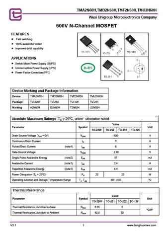
TMA2N60H,TMD2N60H,TMT2N60H,TMU2N60H Wuxi Unigroup Microelectronics Company Wuxi Unigroup Microelectronics Company 600V N-Channel MOSFET FEATURES Fast switching 100% avalanche tested Improved dv/dt capability APPLICATIONS Switch Mode Power Supply (SMPS) Uninterruptible Power Supply (UPS) Power Factor Correction (PFC) Device Marking and Package Info
hm12n60 hm12n60f.pdf
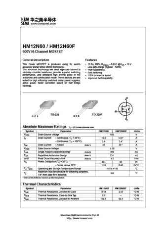
HM12N60 / HM12N60F 600V N-Channel MOSFET General Description Features This Power MOSFET is produced using SL semi s 12.0A, 600V, RDS(on) = 0.65 @VGS = 10 V advanced planar stripe DMOS technology. Low gate charge ( typical 52nC) This advanced technology has been especially tailored to High ruggedness minimize on-state resistance, provide superior switching Fast switc
hm2n60.pdf
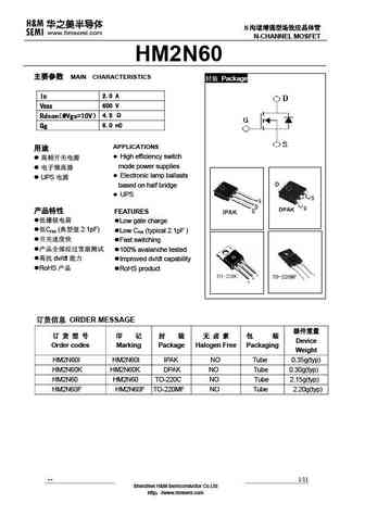
N R N-CHANNEL MOSFET HM2N60 MAIN CHARACTERISTICS Package 2.0 A ID 600 V VDSS Rdson 4.5 @Vgs=10V 6.0 nC Qg APPLICATIONS High efficiency switch mode power supplies Electronic lamp ballasts UPS based on half bridge UPS
mdp2n60 mdt2n60 mpf2n60.pdf
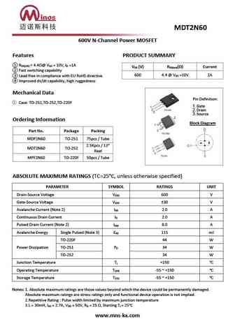
600V N-Channel Power MOSFET Features PRODUCT SUMMARY R
fxn2n60d.pdf
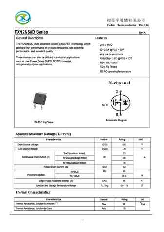
FuXin Semiconductor Co., Ltd. FXN2N60D Series Rev.A General Description Features The FXN2N60D uses advanced Silicon s MOSFET Technology, which VDS = 600V provides high performance in on-state resistance, fast switching ID = 2.3A @VGS = 10V performance, and excellent quality. Very low on-resistance These devices can also be utilized in industr
fxn12n60fs.pdf
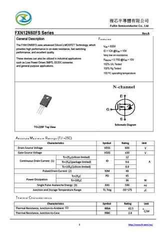
FuXin Semiconductor Co., Ltd. FXN12N60FS Series Rev.A General Description Features The FXN12N60FS uses advanced Silicon s MOSFET Technology, which V = 600V DS provides high performance in on-state resistance, fast switching ID = 12A @V = 10V GS performance, and excellent quality. Very low on-resistance These devices can also be utilized in i
h12n60p h12n60f.pdf
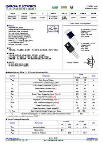
12N60 Series N-Channel MOSFET 12A, 600V, N H FQP12N60C H12N60P P TO-220AB HAOHAI 50Pcs 1000Pcs 5000Pcs 12N60 FQPF12N60C H12N60F F TO-220FP 12N60 Series Pin Assignment Features ID=12A Originative
h2n60p h2n60f.pdf
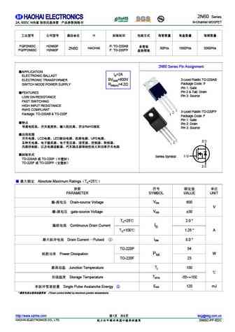
2N60 Series N-Channel MOSFET 2A, 600V, N H FQP2N60C H2N60P P TO-220AB HAOHAI 50Pcs 1000Pcs 5000Pcs 2N60 FQPF2N60C H2N60F F TO-220FP 2N60 Series Pin Assignment APPLICATION ID=2A ELECTRONIC BALLAST
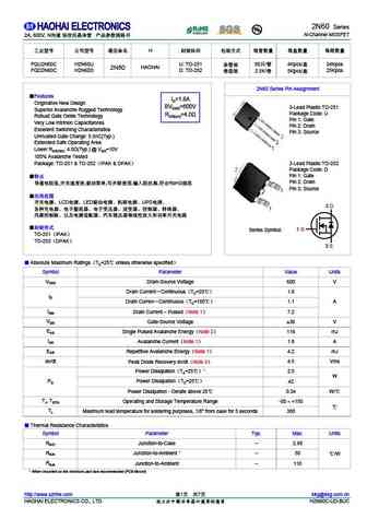
spp02n60c3.pdf
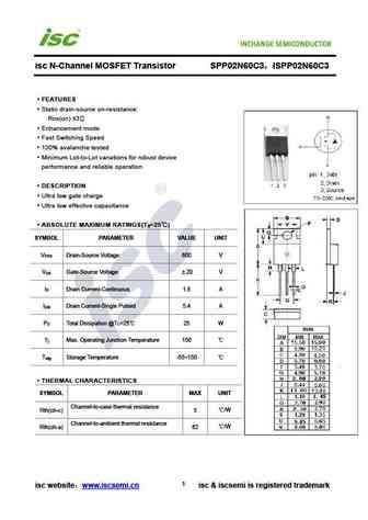
isc N-Channel MOSFET Transistor SPP02N60C3 ISPP02N60C3 FEATURES Static drain-source on-resistance RDS(on) 3 Enhancement mode Fast Switching Speed 100% avalanche tested Minimum Lot-to-Lot variations for robust device performance and reliable operation DESCRIPTION Ultra low gate charge Ultra low effective capacitance ABSOLUTE MAXIMUM RATINGS(T =25 ) a
2n6059.pdf
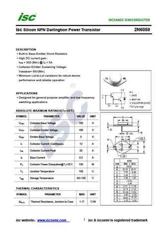
isc Silicon NPN Darlingtion Power Transistor 2N6059 DESCRIPTION Built-in Base-Emitter Shunt Resistors High DC current gain- h = 300 (Min) @ I = 5A FE C Collector-Emitter Sustaining Voltage- V = 80V(Min) CEO(SUS) Minimum Lot-to-Lot variations for robust device performance and reliable operation APPLICATIONS Designed for general purpose amplifier and low frequency switching
aou2n60a.pdf

isc N-Channel MOSFET Transistor AOU2N60A FEATURES Drain Current I = 2A@ T =25 D C Drain Source Voltage- V =600V(Min) DSS Static Drain-Source On-Resistance R =4.7 (Max) DS(on) 100% avalanche tested Minimum Lot-to-Lot variations for robust device performance and reliable operation DESCRIPTION Designed for use in switch mode power supplies and general purpose
2n6029 2n6030.pdf
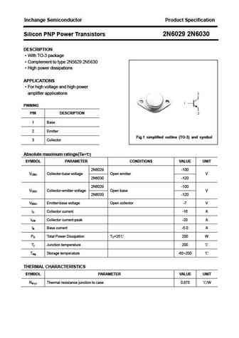
Inchange Semiconductor Product Specification Silicon PNP Power Transistors 2N6029 2N6030 DESCRIPTION With TO-3 package Complement to type 2N5629 2N5630 High power dissipations APPLICATIONS For high voltage and high power amplifier applications PINNING PIN DESCRIPTION 1 Base 2 Emitter Fig.1 simplified outline (TO-3) and symbol 3 Collector Absolute maximum rating
spd02n60s5.pdf
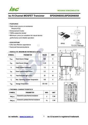
isc N-Channel MOSFET Transistor SPD02N60S5,ISPD02N60S5 FEATURES Static drain-source on-resistance RDS(on) 3 Enhancement mode 100% avalanche tested Minimum Lot-to-Lot variations for robust device performance and reliable operation DESCRITION Ultra low effective capacitance Improved transconductance ABSOLUTE MAXIMUM RATINGS(T =25 ) a SYMBOL PARAMETER VALUE
2n6053 2n6054.pdf
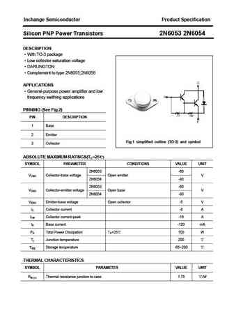
Inchange Semiconductor Product Specification Silicon PNP Power Transistors 2N6053 2N6054 DESCRIPTION With TO-3 package Low collector saturation voltage DARLINGTON Complement to type 2N6055;2N6056 APPLICATIONS General-purpose power amplifier and low frequency swithing applications PINNING (See Fig.2) PIN DESCRIPTION 1 Base 2 Emitter Fig.1 simplified outline (T
2n6032.pdf

isc Silicon NPN Power Transistor 2N6032 DESCRIPTION Collector-Emitter Breakdown Voltage- V =90V(Min) (BR)CEO Minimum Lot-to-Lot variations for robust device Performance and reliable operation APPLICATIONS Power amplifier and switching applications ABSOLUTE MAXIMUM RATINGS(Ta=25 ) UNI SYMBOL PARAMETER VALUE T V Collector-Base Voltage 120 V CBO V Collector-Emitter Voltage
2n6054.pdf
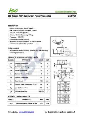
INCHANGE Semiconductor isc Silicon PNP Darlingtion Power Transistor 2N6054 DESCRIPTION Built-in Base-Emitter Shunt Resistors Low Collector-Emitter Saturation Voltage V = -2.0V(Max)@ I = -4A CE(sat) C Collector-Emitter Sustaining Voltage- V = -80V(Min) CEO(SUS) Complement to type 2N6056 Minimum Lot-to-Lot variations for robust device performance and reliable operation
2n6034 2n6035 2n6036.pdf
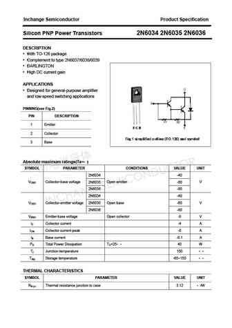
Inchange Semiconductor Product Specification Silicon PNP Power Transistors 2N6034 2N6035 2N6036 DESCRIPTION With TO-126 package Complement to type 2N6037/6038/6039 DARLINGTON High DC current gain APPLICATIONS Designed for general-purpose amplifier and low-speed switching applications PINNING(see Fig.2) PIN DESCRIPTION 1 Emitter 2 Collector 3 Base Absolute ma
2n6031.pdf
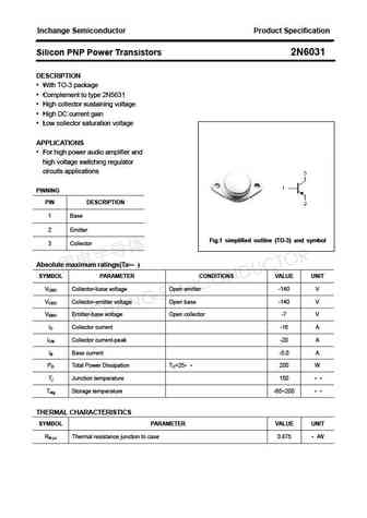
Inchange Semiconductor Product Specification Silicon PNP Power Transistors 2N6031 DESCRIPTION With TO-3 package Complement to type 2N5631 High collector sustaining voltage High DC current gain Low collector saturation voltage APPLICATIONS For high power audio amplifier and high voltage switching regulator circuits applications PINNING PIN DESCRIPTION 1 Bas
aoi2n60.pdf
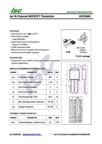
isc N-Channel MOSFET Transistor AOI2N60 FEATURES Drain Current I = 2A@ T =25 D C Drain Source Voltage- V =600V(Min) DSS Static Drain-Source On-Resistance R =4.4 (Max) DS(on) 100% avalanche tested Minimum Lot-to-Lot variations for robust device performance and reliable operation DESCRIPTION Designed for use in switch mode power supplies and general purpose a
2n6039.pdf
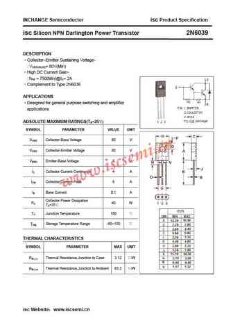
INCHANGE Semiconductor isc Product Specification isc Silicon NPN Darlington Power Transistor 2N6039 DESCRIPTION Collector Emitter Sustaining Voltage- VCEO(SUS)= 80V(Min) High DC Current Gain- hFE = 750(Min)@IC= 2A Complement to Type 2N6036 APPLICATIONS Designed for general purpose switching and amplifier applications ABSOLUTE MAXIMUM RATINGS(Ta=25 ) SYMBO
aot12n60.pdf

isc N-Channel MOSFET Transistor AOT12N60 FEATURES Drain Current I =12A@ T =25 D C Drain Source Voltage- V =600V(Min) DSS Static Drain-Source On-Resistance R = 0.55 (Max) DS(on) 100% avalanche tested Minimum Lot-to-Lot variations for robust device performance and reliable operation DESCRIPTION Designed for use in switch mode power supplies and general purpos
2n6037 2n6038 2n6039.pdf
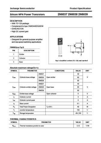
Inchange Semiconductor Product Specification Silicon NPN Power Transistors 2N6037 2N6038 2N6039 DESCRIPTION With TO-126 package Complement to type 2N6034/6035/6036 DARLINGTON High DC current gain APPLICATIONS Designed for general-purpose amplifier and low-speed switching applications PINNING(see Fig.2) PIN DESCRIPTION 1 Emitter 2 Collector 3 Base Absolute ma
2n6098 2n6099 2n6100 2n6101.pdf
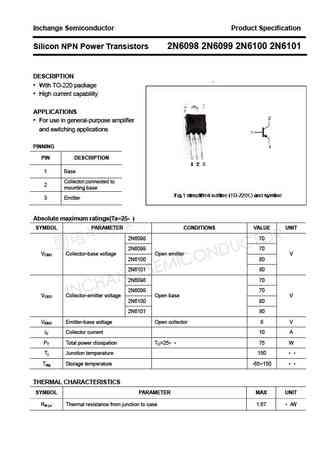
Inchange Semiconductor Product Specification Silicon NPN Power Transistors 2N6098 2N6099 2N6100 2N6101 DESCRIPTION With TO-220 package High current capability APPLICATIONS For use in general-purpose amplifier and switching applications PINNING PIN DESCRIPTION 1 Base Collector;connected to 2 mounting base 3 Emitter Absolute maximum ratings(Ta=25 ) SYMBOL PA
2n6057.pdf
INCHANGE Semiconductor isc Product Specification isc Silicon NPN Darlingtion Power Transistor 2N6057 DESCRIPTION Built-in Base-Emitter Shunt Resistors High DC current gain- hFE = 750 (Min) @ IC = 6A Collector-Emitter Sustaining Voltage- VCEO(SUS)= 60V(Min) Complement to type 2N6050 APPLICATIONS Designed for general purpose amplifier and low frequency switching ap
12n60-263.pdf
INCHANGE Semiconductor Isc N-Channel MOSFET Transistor 12N60 FEATURES With To-263(D2PAK) package Low input capacitance and gate charge Low gate input resistance 100% avalanche tested Minimum Lot-to-Lot variations for robust device performance and reliable operation APPLICATIONS Switching applications Designed for high efficiency switch mode power supply ABSOLUTE
2n6045g.pdf
INCHANGE Semiconductor isc Silicon NPN Darlington Power Transistor 2N6045G DESCRIPTION High DC Current Gain- h = 1000(Min)@ I = 3A FE C Collector-Emitter Sustaining Voltage- V = 100V(Min) CEO(SUS) Low Collector-Emitter Saturation Voltage- V = 2.0V(Max)@ I = 3A CE(sat) C Complement to Type 2N6042 G Pb-Free package Minimum Lot-to-Lot variations for robust device
spu02n60c3.pdf
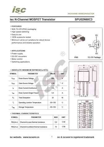
isc N-Channel MOSFET Transistor SPU02N60C3 FEATURES With TO-251(IPAK) packaging High speed switching Easy to use 100% avalanche tested Minimum Lot-to-Lot variations for robust device performance and reliable operation APPLICATIONS Power supply DC-DC converters Motor control Switching applications ABSOLUTE MAXIMUM RATINGS(T =25 ) a SYMBOL PARAMETER VALUE
aod2n60.pdf
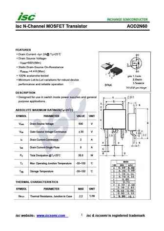
isc N-Channel MOSFET Transistor AOD2N60 FEATURES Drain Current I = 2A@ T =25 D C Drain Source Voltage- V =600V(Min) DSS Static Drain-Source On-Resistance R =4.4 (Max) DS(on) 100% avalanche tested Minimum Lot-to-Lot variations for robust device performance and reliable operation DESCRIPTION Designed for use in switch mode power supplies and general purpose a
aotf12n60.pdf
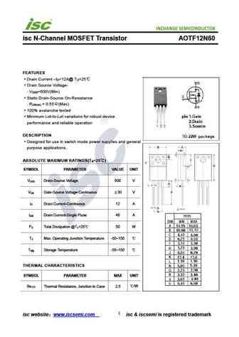
isc N-Channel MOSFET Transistor AOTF12N60 FEATURES Drain Current I =12A@ T =25 D C Drain Source Voltage- V =600V(Min) DSS Static Drain-Source On-Resistance R = 0.55 (Max) DS(on) 100% avalanche tested Minimum Lot-to-Lot variations for robust device performance and reliable operation DESCRIPTION Designed for use in switch mode power supplies and general purpo
aou2n60.pdf

isc N-Channel MOSFET Transistor AOU2N60 FEATURES Drain Current I = 2A@ T =25 D C Drain Source Voltage- V =600V(Min) DSS Static Drain-Source On-Resistance R =4.4 (Max) DS(on) 100% avalanche tested Minimum Lot-to-Lot variations for robust device performance and reliable operation DESCRIPTION Designed for use in switch mode power supplies and general purpose a
2n6056.pdf
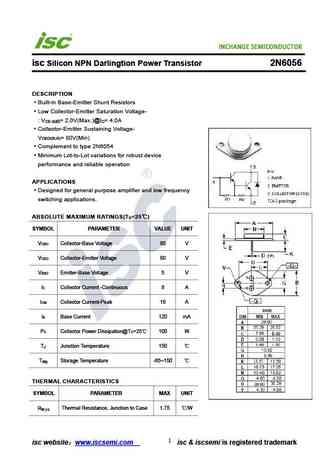
INCHANGE Semiconductor isc Silicon NPN Darlingtion Power Transistor 2N6056 DESCRIPTION Built-in Base-Emitter Shunt Resistors Low Collector-Emitter Saturation Voltage- V = 2.0V(Max.)@I = 4.0A CE (sat) C Collector-Emitter Sustaining Voltage- V = 80V(Min) CEO(SUS) Complement to type 2N6054 Minimum Lot-to-Lot variations for robust device performance and reliable operation A
2n6049.pdf
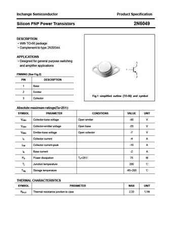
Inchange Semiconductor Product Specification Silicon PNP Power Transistors 2N6049 DESCRIPTION With TO-66 package Complement to type 2N3054A APPLICATIONS Designed for general purpose switching and amplifier applications PINNING (See Fig.2) PIN DESCRIPTION 1 Base 2 Emitter Fig.1 simplified outline (TO-66) and symbol 3 Collector Absolute maximum ratings(Ta=25 ) SY
12n60.pdf
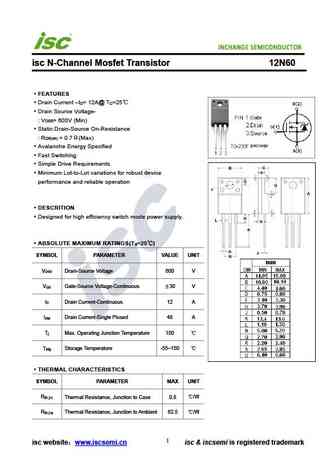
isc N-Channel Mosfet Transistor 12N60 FEATURES Drain Current I = 12A@ T =25 D C Drain Source Voltage- V = 600V (Min) DSS Static Drain-Source On-Resistance R = 0.7 (Max) DS(on) Avalanche Energy Specified Fast Switching Simple Drive Requirements Minimum Lot-to-Lot variations for robust device performance and reliable operation DESCRITION Designed for
aot12n60fd.pdf
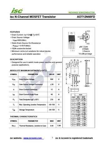
isc N-Channel MOSFET Transistor AOT12N60FD FEATURES Drain Current I =12A@ T =25 D C Drain Source Voltage- V =600V(Min) DSS Static Drain-Source On-Resistance R = 0.65 (Max) DS(on) 100% avalanche tested Minimum Lot-to-Lot variations for robust device performance and reliable operation DESCRIPTION Designed for use in switch mode power supplies and general purp
2n6055 2n6056.pdf
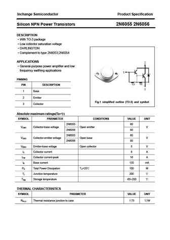
Inchange Semiconductor Product Specification Silicon NPN Power Transistors 2N6055 2N6056 DESCRIPTION With TO-3 package Low collector saturation voltage DARLINGTON Complement to type 2N6053;2N6054 APPLICATIONS General-purpose power amplifier and low frequency swithing applications PINNING PIN DESCRIPTION 1 Base 2 Emitter Fig.1 simplified outline (TO-3) and sy
2n6052.pdf
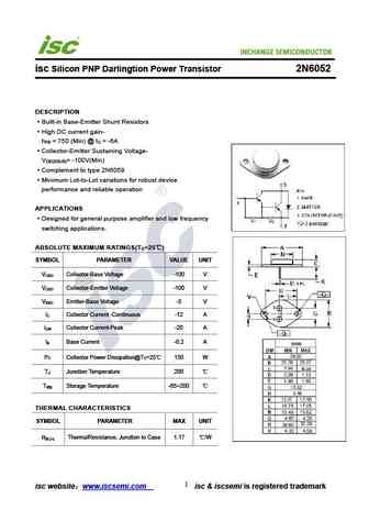
INCHANGE Semiconductor isc Silicon PNP Darlingtion Power Transistor 2N6052 DESCRIPTION Built-in Base-Emitter Shunt Resistors High DC current gain- h = 750 (Min) @ I = -6A FE C Collector-Emitter Sustaining Voltage- V = -100V(Min) CEO(SUS) Complement to type 2N6059 Minimum Lot-to-Lot variations for robust device performance and reliable operation APPLICATIONS Designed fo
fch072n60f.pdf
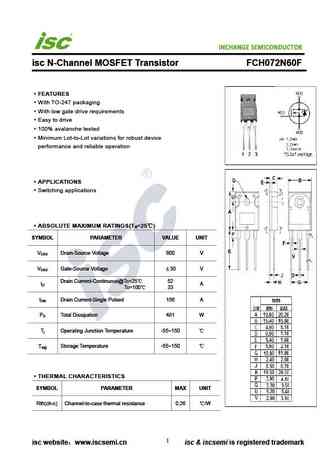
INCHANGE Semiconductor isc N-Channel MOSFET Transistor FCH072N60F FEATURES With TO-247 packaging With low gate drive requirements Easy to drive 100% avalanche tested Minimum Lot-to-Lot variations for robust device performance and reliable operation APPLICATIONS Switching applications ABSOLUTE MAXIMUM RATINGS(T =25 ) a SYMBOL PARAMETER VALUE UNIT V Drain-Source
aotf12n60fd.pdf
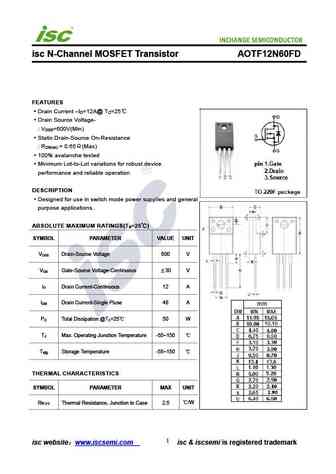
isc N-Channel MOSFET Transistor AOTF12N60FD FEATURES Drain Current I =12A@ T =25 D C Drain Source Voltage- V =600V(Min) DSS Static Drain-Source On-Resistance R = 0.65 (Max) DS(on) 100% avalanche tested Minimum Lot-to-Lot variations for robust device performance and reliable operation DESCRIPTION Designed for use in switch mode power supplies and general pur
aob12n60fd.pdf
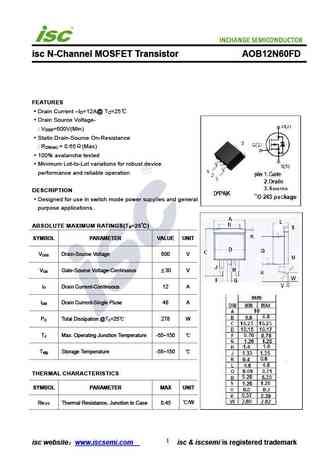
isc N-Channel MOSFET Transistor AOB12N60FD FEATURES Drain Current I =12A@ T =25 D C Drain Source Voltage- V =600V(Min) DSS Static Drain-Source On-Resistance R = 0.65 (Max) DS(on) 100% avalanche tested Minimum Lot-to-Lot variations for robust device performance and reliable operation DESCRIPTION Designed for use in switch mode power supplies and general purp
jcs2n60f.pdf
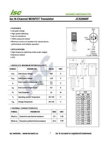
INCHANGE Semiconductor Isc N-Channel MOSFET Transistor JCS2N60F FEATURES Low gate charge High speed switching Low on-resistance 100% avalanche tested Minimum Lot-to-Lot variations for robust device performance and reliable operation APPLICATIONS High frequency switching mode power supply Electronic ballast UPS ABSOLUTE MAXIMUM RATINGS(T =25 ) a SYMBOL PARA
aot2n60.pdf
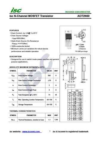
isc N-Channel MOSFET Transistor AOT2N60 FEATURES Drain Current I = 2A@ T =25 D C Drain Source Voltage- V =600V(Min) DSS Static Drain-Source On-Resistance R =4.4 (Max) DS(on) 100% avalanche tested Minimum Lot-to-Lot variations for robust device performance and reliable operation DESCRIPTION Designed for use in switch mode power supplies and general purpose a
spb02n60c3.pdf

Isc N-Channel MOSFET Transistor SPB02N60C3 FEATURES With To-263(D2PAK) package Low input capacitance and gate charge Low gate input resistance 100% avalanche tested Minimum Lot-to-Lot variations for robust device performance and reliable operation APPLICATIONS Switching applications ABSOLUTE MAXIMUM RATINGS(T =25 ) a SYMBOL PARAMETER VALUE UNIT V Drain-Source Vo
spp02n60s5.pdf
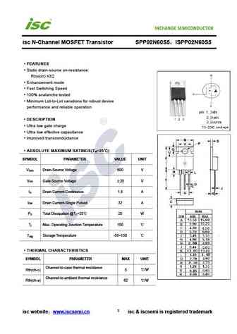
isc N-Channel MOSFET Transistor SPP02N60S5 ISPP02N60S5 FEATURES Static drain-source on-resistance RDS(on) 3 Enhancement mode Fast Switching Speed 100% avalanche tested Minimum Lot-to-Lot variations for robust device performance and reliable operation DESCRIPTION Ultra low gate charge Ultra low effective capacitance Improved transconductance ABSOLUTE M
2n6098.pdf
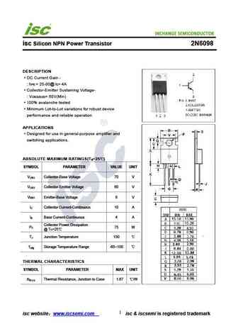
isc Silicon NPN Power Transistor 2N6098 DESCRIPTION DC Current Gain - h = 20-80@ I = 4A FE C Collector-Emitter Sustaining Voltage- V = 60V(Min) CEO(SUS) 100% avalanche tested Minimum Lot-to-Lot variations for robust device performance and reliable operation APPLICATIONS Designed for use in general-purpose amplifier and switching applications. ABSOLUTE MAXIMUM RATINGS
2n6033.pdf
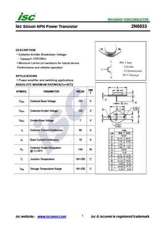
isc Silicon NPN Power Transistor 2N6033 DESCRIPTION Collector-Emitter Breakdown Voltage- V =-120V(Min) (BR)CEO Minimum Lot-to-Lot variations for robust device Performance and reliable operation APPLICATIONS Power amplifier and switching applications ABSOLUTE MAXIMUM RATINGS(Ta=25 ) UNI SYMBOL PARAMETER VALUE T V Collector-Base Voltage 150 V CBO V Collector-Emitter Volta
fqpf12n60c.pdf
isc N-Channel Mosfet Transistor FQPF12N60C FEATURES Drain Current I = 12A@ T =25 D C Drain Source Voltage- V = 600V(Min) DSS Static Drain-Source On-Resistance R = 0.65 (Max) DS(on) 100% avalanche tested Minimum Lot-to-Lot variations for robust device performance and reliable operation DESCRITION Designed for high efficiency switch mode power supply. A
2n6043 2n6044 2n6045.pdf
Inchange Semiconductor Product Specification Silicon NPN Power Transistors 2N6043 2N6044 2N6045 DESCRIPTION With TO-220C package Complement to type 2N6040/6041/6042 DARLINGTON High DC current gain Low collector saturation voltage APPLICATIONS For general-purpose amplifier and low-speed switching applications PINNING PIN DESCRIPTION 1 Base Collector;co
spd02n60c3.pdf
isc N-Channel MOSFET Transistor SPD02N60C3,ISPD02N60C3 FEATURES Static drain-source on-resistance RDS(on) 3 Enhancement mode 100% avalanche tested Minimum Lot-to-Lot variations for robust device performance and reliable operation DESCRITION Ultra low effective capacitance ABSOLUTE MAXIMUM RATINGS(T =25 ) a SYMBOL PARAMETER VALUE UNIT V Drain-Source Voltage
aow12n60.pdf
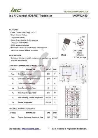
isc N-Channel MOSFET Transistor AOW12N60 FEATURES Drain Current I =12A@ T =25 D C Drain Source Voltage- V =600V(Min) DSS Static Drain-Source On-Resistance R = 0.55 (Max) DS(on) 100% avalanche tested Minimum Lot-to-Lot variations for robust device performance and reliable operation DESCRIPTION Designed for use in switch mode power supplies and general purpos
2n6078.pdf
isc Silicon NPN Power Transistor 2N6078 DESCRIPTION Low Collector-Emitter Sustaining Voltage High voltage Low Collector-Emitter Saturation Voltage- 100% avalanche tested Minimum Lot-to-Lot variations for robust device performance and reliable operation APPLICATIONS Linear applications Power switching circuits ABSOLUTE MAXIMUM RATINGS (T =25 ) a SYMBOL PARAMETER VALU
spu02n60s5.pdf

isc N-Channel MOSFET Transistor SPU02N60S5 FEATURES With TO-251(IPAK) packaging High speed switching Easy to use 100% avalanche tested Minimum Lot-to-Lot variations for robust device performance and reliable operation APPLICATIONS Power supply DC-DC converters Motor control Switching applications ABSOLUTE MAXIMUM RATINGS(T =25 ) a SYMBOL PARAMETER VALUE
aoy2n60.pdf

isc N-Channel MOSFET Transistor AOY2N60 FEATURES Drain Current I = 2A@ T =25 D C Drain Source Voltage- V =600V(Min) DSS Static Drain-Source On-Resistance R =4.7 (Max) DS(on) 100% avalanche tested Minimum Lot-to-Lot variations for robust device performance and reliable operation DESCRIPTION Designed for use in switch mode power supplies and general purpose a
aoi2n60a.pdf

isc N-Channel MOSFET Transistor AOI2N60A FEATURES Drain Current I = 2A@ T =25 D C Drain Source Voltage- V =600V(Min) DSS Static Drain-Source On-Resistance R =4.7 (Max) DS(on) 100% avalanche tested Minimum Lot-to-Lot variations for robust device performance and reliable operation DESCRIPTION Designed for use in switch mode power supplies and general purpose
irfp22n60k.pdf
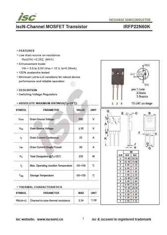
iscN-Channel MOSFET Transistor IRFP22N60K FEATURES Low drain-source on-resistance RDS(ON) =0.28 (MAX) Enhancement mode Vth = 3.0 to 5.0V (VDS = 10 V, ID=0.25mA) 100% avalanche tested Minimum Lot-to-Lot variations for robust device performance and reliable operation DESCRITION Switching Voltage Regulators ABSOLUTE MAXIMUM RATINGS(T =25 ) a SYMBOL PARAMETER VAL
spb02n60s5.pdf
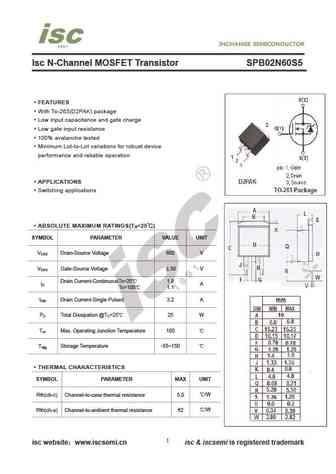
Isc N-Channel MOSFET Transistor SPB02N60S5 FEATURES With To-263(D2PAK) package Low input capacitance and gate charge Low gate input resistance 100% avalanche tested Minimum Lot-to-Lot variations for robust device performance and reliable operation APPLICATIONS Switching applications ABSOLUTE MAXIMUM RATINGS(T =25 ) a SYMBOL PARAMETER VALUE UNIT V Drain-Source Vo
2n6058 2n6059.pdf
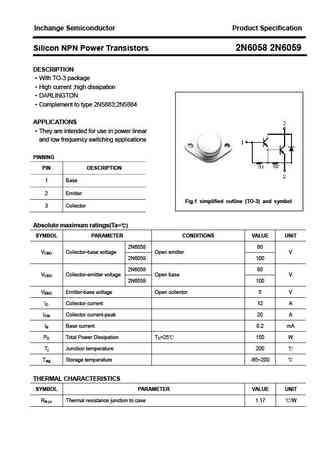
Inchange Semiconductor Product Specification Silicon NPN Power Transistors 2N6058 2N6059 DESCRIPTION With TO-3 package High current ;high dissipation DARLINGTON Complement to type 2N5883;2N5884 APPLICATIONS They are intended for use in power linear and low frequency switching applications PINNING PIN DESCRIPTION 1 Base 2 Emitter Fig.1 simplified outline (TO-
sihb22n60e.pdf
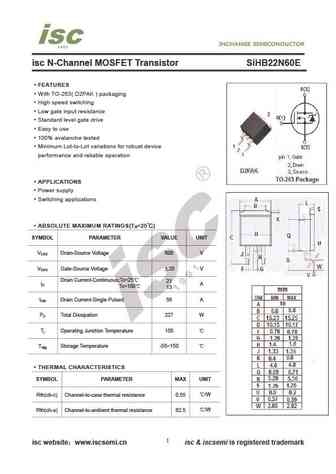
isc N-Channel MOSFET Transistor SiHB22N60E FEATURES With TO-263( D2PAK ) packaging High speed switching Low gate input resistance Standard level gate drive Easy to use 100% avalanche tested Minimum Lot-to-Lot variations for robust device performance and reliable operation APPLICATIONS Power supply Switching applications ABSOLUTE MAXIMUM RATINGS(T =25 ) a
2n6077 2n6078 2n6079.pdf
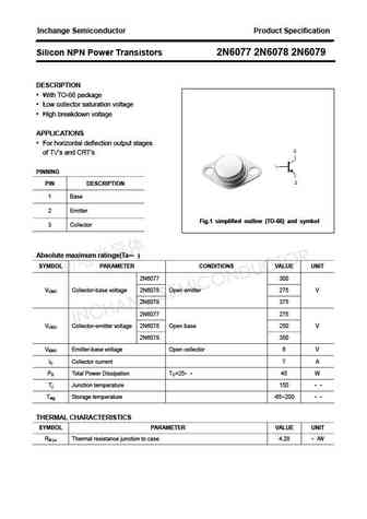
Inchange Semiconductor Product Specification Silicon NPN Power Transistors 2N6077 2N6078 2N6079 DESCRIPTION With TO-66 package Low collector saturation voltage High breakdown voltage APPLICATIONS For horizontal deflection output stages of TV s and CRT s PINNING PIN DESCRIPTION 1 Base 2 Emitter Fig.1 simplified outline (TO-66) and symbol 3 Collector Absolut
aod2n60a.pdf
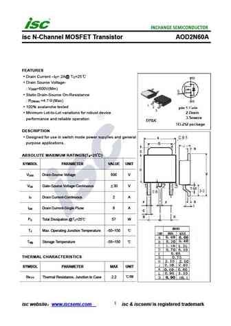
isc N-Channel MOSFET Transistor AOD2N60A FEATURES Drain Current I = 2A@ T =25 D C Drain Source Voltage- V =600V(Min) DSS Static Drain-Source On-Resistance R =4.7 (Max) DS(on) 100% avalanche tested Minimum Lot-to-Lot variations for robust device performance and reliable operation DESCRIPTION Designed for use in switch mode power supplies and general purpose
2n6036.pdf
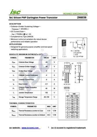
INCHANGE Semiconductor isc Silicon PNP Darlington Power Transistor 2N6036 DESCRIPTION Collector Emitter Sustaining Voltage V = CEO(SUS) -80V(Min.) DC Current Gain h = 750(Min) @ I = -2A FE C Complement to Type 2N6039 Minimum Lot-to-Lot variations for robust device performance and reliable operation APPLICATIONS Designed for general-purpose amplifier and low-sp
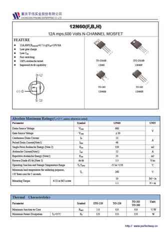
Другие IGBT... 22N60, UF601, UK2996, 1N60A, 1N60, 1N60P, 1N60Z, 2N60L, IRF540, 2N60K, 3N60, 3N60A, 3N60Z, 3N60K, 4N60, 4N60Z, 4N60K
🌐 : EN ES РУ

Список транзисторов
Обновления
MOSFET: CS65N25AKR | AOL1718 | BCD70N07A | BCD90N03 | BCD80N06 | T50N06 | H50N06 | BCD12N65 | BCT12N65 | BCD4N65 | BCT4N65 | BCD7N65 | BCT7N65 | BCT20N65 | ASDM30P100KQ | ASDM30N90Q
Popular searches
tip122 transistor | 2sc1079 | 2sc1815 equivalent | 2sa1220 | 2sa940 | 2sc627 | 2sc680 | 2sd234