2N50 datasheet, аналоги, основные параметры
Наименование производителя: 2N50 📄📄
Тип транзистора: MOSFET
Полярность: N
Предельные значения
Pd ⓘ - Максимальная рассеиваемая мощность: 50 W
|Vds|ⓘ - Максимально допустимое напряжение сток-исток: 500 V
|Vgs|ⓘ - Максимально допустимое напряжение затвор-исток: 30 V
|Id| ⓘ - Максимально допустимый постоянный ток стока: 2 A
Tj ⓘ - Максимальная температура канала: 150 °C
Электрические характеристики
tr ⓘ - Время нарастания: 20 ns
Cossⓘ - Выходная емкость: 40 pf
RDSonⓘ - Сопротивление сток-исток открытого транзистора: 3.9 Ohm
📄📄 Копировать
Аналог (замена) для 2N50
- подборⓘ MOSFET транзистора по параметрам
2N50 даташит
2n50.pdf
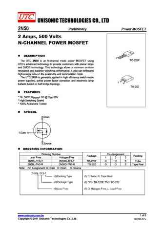
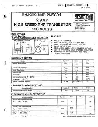
UNISONIC TECHNOLOGIES CO., LTD 2N50 Power MOSFET Preliminary 2 Amps, 500 Volts N-CHANNEL POWER MOSFET DESCRIPTION 1 TO-220F The UTC 2N50 is an N-channel mode power MOSFET using UTC s advanced technology to provide customers with planar stripe and DMOS technology. This technology allows a minimum on-state resistance and superior switching performance. It also can withstan
hgth12n40c1d hgth12n40e1d hgth12n50c1d hgth12n50e1d.pdf
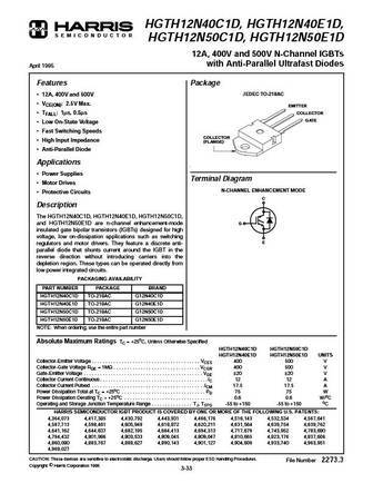
HGTH12N40C1D, HGTH12N40E1D, S E M I C O N D U C T O R HGTH12N50C1D, HGTH12N50E1D 12A, 400V and 500V N-Channel IGBTs with Anti-Parallel Ultrafast Diodes April 1995 Features Package JEDEC TO-218AC 12A, 400V and 500V VCE(ON) 2.5V Max. EMITTER TFALL 1 s, 0.5 s COLLECTOR GATE Low On-State Voltage Fast Switching Speeds COLLECTOR High Input Impedance (FLANG
hgth12n40c1 hgth12n40e1 hgth12n50c1 hgth12n50e1 hgtm12n40c1 hgtm12n40e1 hgtm12n50c1 hgtm12n50e1 hgtp10n40c1 hgtp10n40e1 hgtp10n50c1 hgtp10n50e1.pdf
std2n50 std2n50-1 std2n50t4.pdf
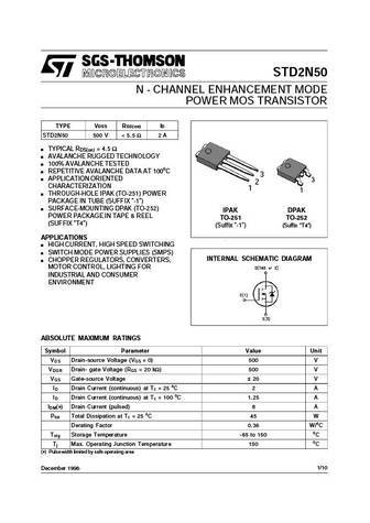
STD2N50 N - CHANNEL ENHANCEMENT MODE POWER MOS TRANSISTOR TYPE V R I DSS DS(on) D STD2N50 500 V
hgth12n40c1 hgth12n40e1 hgth12n50c1 hgth12n50e1 hgtp10n40c1 hgtp10n40e1 hgtp10n50c1 hgtp10n50e1.pdf
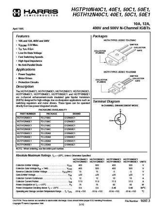
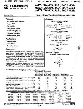
HGTP10N40C1, 40E1, 50C1, 50E1, S E M I C O N D U C T O R HGTH12N40C1, 40E1, 50C1, 50E1 10A, 12A, 400V and 500V N-Channel IGBTs April 1995 Features Packages HGTH-TYPES JEDEC TO-218AC 10A and 12A, 400V and 500V EMITTER VCE(ON) 2.5V Max. COLLECTOR TFI 1 s, 0.5 s GATE COLLECTOR (FLANGE) Low On-State Voltage Fast Switching Speeds High Input Impedance
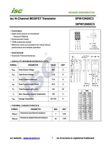
spa12n50c3 spi12n50c3 spp12n50c3.pdf
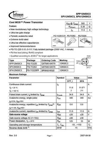
SPP12N50C3 SPI12N50C3, SPA12N50C3 Cool MOS Power Transistor VDS @ Tjmax 560 V Feature RDS(on) 0.38 New revolutionary high voltage technology ID 11.6 A Ultra low gate charge PG-TO220-3-31 PG-TO262- PG-TO220 Periodic avalanche rated 2 Extreme dv/dt rated 3 Ultra low effective capacitances 2 3 2 1 1 P-TO220-3-31 Improved transconductance P-TO220-3
ixth12n45ma ixth12n45mb ixth12n50ma ixth12n50mb ixth15n35ma ixth15n35mb ixth15n40ma ixth15n40mb ixtz42n20mb ixtz67n10ma ixtz67n10mb.pdf
mtp2n50e.pdf
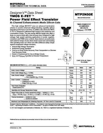
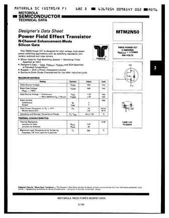
MOTOROLA Order this document SEMICONDUCTOR TECHNICAL DATA by MTP2N50E/D Designer's Data Sheet MTP2N50E TMOS E-FET. Motorola Preferred Device Power Field Effect Transistor N Channel Enhancement Mode Silicon Gate TMOS POWER FET This high voltage MOSFET uses an advanced termination 2.0 AMPERES scheme to provide enhanced voltage blocking capability without 500 VOLTS degra
2n5087rev0.pdf
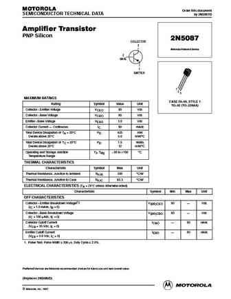
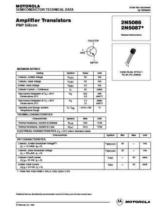
MOTOROLA Order this document SEMICONDUCTOR TECHNICAL DATA by 2N5087/D Amplifier Transistor PNP Silicon 2N5087 COLLECTOR 3 Motorola Preferred Device 2 BASE 1 EMITTER 1 2 3 MAXIMUM RATINGS CASE 29 04, STYLE 1 Rating Symbol Value Unit TO 92 (TO 226AA) Collector Emitter Voltage VCEO 50 Vdc Collector Base Voltage VCBO 50 Vdc Emitter Base Voltage VEBO 3.0 Vdc Colle
mtd2n50erev1x.pdf
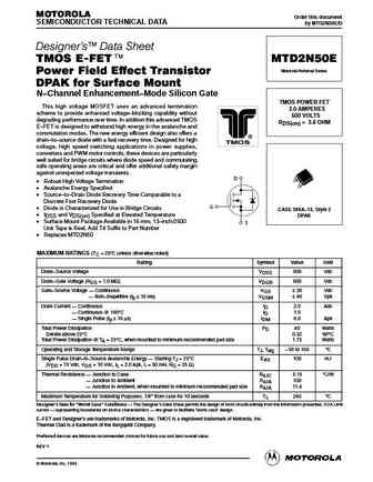
MOTOROLA Order this document SEMICONDUCTOR TECHNICAL DATA by MTD2N50E/D Designer's Data Sheet TMOS E-FET. MTD2N50E Motorola Preferred Device Power Field Effect Transistor DPAK for Surface Mount N Channel Enhancement Mode Silicon Gate TMOS POWER FET This high voltage MOSFET uses an advanced termination 2.0 AMPERES scheme to provide enhanced voltage blocking capability wi
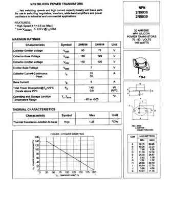
2n5038 2n5039.pdf
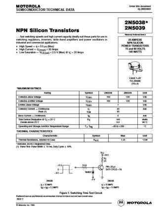
Order this document MOTOROLA by 2N5038/D SEMICONDUCTOR TECHNICAL DATA 2N5038 * 2N5039 NPN Silicon Transistors *Motorola Preferred Device . . . fast switching speeds and high current capacity ideally suit these parts for use in switching regulators, inverters, wide band amplifiers and power oscillators in 20 AMPERE industrial and commercial applications. NPN SILICON POWER TRANSIS
mtd2n50e.pdf

MOTOROLA Order this document SEMICONDUCTOR TECHNICAL DATA by MTD2N50E/D Designer's Data Sheet TMOS E-FET. MTD2N50E Motorola Preferred Device Power Field Effect Transistor DPAK for Surface Mount N Channel Enhancement Mode Silicon Gate TMOS POWER FET This high voltage MOSFET uses an advanced termination 2.0 AMPERES scheme to provide enhanced voltage blocking capability wi
2n5086 2n5087.pdf
MOTOROLA Order this document SEMICONDUCTOR TECHNICAL DATA by 2N5086/D Amplifier Transistors 2N5086 PNP Silicon * 2N5087 *Motorola Preferred Device COLLECTOR 3 2 BASE 1 EMITTER 1 2 3 MAXIMUM RATINGS CASE 29 04, STYLE 1 Rating Symbol Value Unit TO 92 (TO 226AA) Collector Emitter Voltage VCEO 50 Vdc Collector Base Voltage VCBO 50 Vdc Emitter Base Voltage VEBO 3.
2n5060 2n5062 2n5061 2n5064.pdf
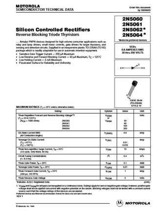
MOTOROLA Order this document SEMICONDUCTOR TECHNICAL DATA by 2N5060/D 2N5060 2N5061 * Silicon Controlled Rectifiers 2N5062 Reverse Blocking Triode Thyristors * 2N5064 *Motorola preferred devices . . . Annular PNPN devices designed for high volume consumer applications such as relay and lamp drivers, small motor controls, gate drivers for larger thyristors, and SCRs sensing and de
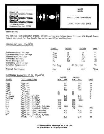
2n5088 2n5089.pdf
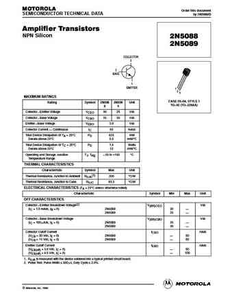
MOTOROLA Order this document SEMICONDUCTOR TECHNICAL DATA by 2N5088/D Amplifier Transistors NPN Silicon 2N5088 2N5089 COLLECTOR 3 2 BASE 1 EMITTER 1 2 3 MAXIMUM RATINGS CASE 29 04, STYLE 1 Rating Symbol 2N508 2N508 Unit TO 92 (TO 226AA) 8 9 Collector Emitter Voltage VCEO 30 25 Vdc Collector Base Voltage VCBO 35 30 Vdc Emitter Base Voltage VEBO 3.0 Vdc Collec
irfp32n50ks.pdf

PD - 94360 IRFP32N50KS SMPS MOSFET HEXFET Power MOSFET Applications Switch Mode Power Supply (SMPS) VDSS RDS(on)typ. ID Uninterruptible Power Supply High Speed Power Switching 500V 0.135 32A Hard Switched and High Frequency Circuits Benefits Low Gate Charge Qg results in Simple Drive Requirement Improved Gate, Avalanche and Dynamic dv/dt Ruggedness Fully Characterize
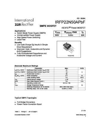
irfp22n50a.pdf
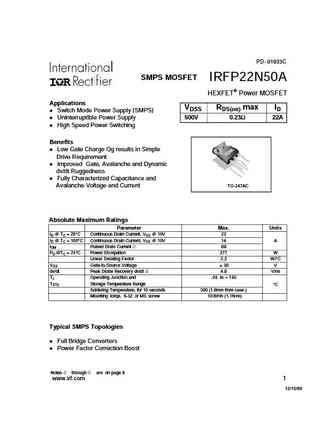
PD- 91833C SMPS MOSFET IRFP22N50A HEXFET Power MOSFET Applications VDSS RDS(on) max ID Switch Mode Power Supply (SMPS) UninterruptIble Power Supply 500V 0.23 22A High Speed Power Switching Benefits Low Gate Charge Qg results in Simple Drive Requirement Improved Gate, Avalanche and Dynamic dv/dt Ruggedness Fully Characterized Capacitance and Avalanche Voltage and Curren
irfba32n50k.pdf
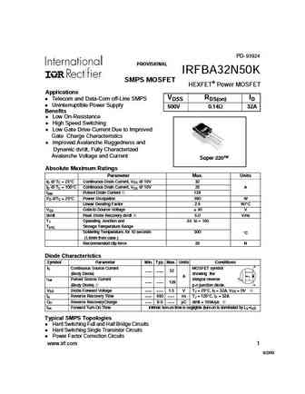
PD- 93924 PROVISIONAL IRFBA32N50K SMPS MOSFET HEXFET Power MOSFET Applications VDSS RDS(on) ID Telecom and Data-Com off-Line SMPS UninterruptIble Power Supply 500V 0.14 32A Benefits Low On-Resistance High Speed Switching Low Gate Drive Current Due to Improved Gate Charge Characteristics Improved Avalanche Ruggedness and Dynamic dv/dt, Fully Characterized Avalanche Vo
irfp32n50kpbf.pdf
PD - 95052 IRFP32N50KPbF SMPS MOSFET HEXFET Power MOSFET AppIications l Switch Mode Power Supply (SMPS) VDSS RDS(on)typ. ID l Uninterruptible Power Supply l High Speed Power Switching 500V 0.135 32A l Hard Switched and High Frequency Circuits l Lead-Free Benefits l Low Gate Charge Qg results in Simple Drive Requirement l Improved Gate, Avalanche and Dynamic dv/dt Ruggednes
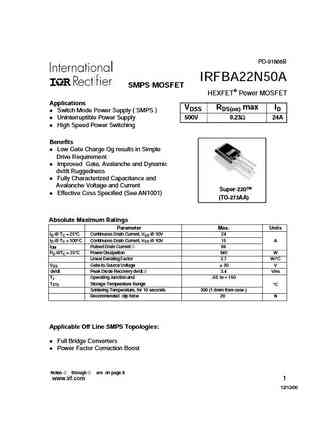
irfba22n50apbf.pdf

PD-91886C IRFBA22N50A SMPS MOSFET HEXFET Power MOSFET Applications VDSS RDS(on) max ID l Switch Mode Power Supply ( SMPS ) l Uninterruptible Power Supply 500V 0.23 24A l High Speed Power Switching Benefits l Low Gate Charge Qg results in Simple Drive Requirement l Improved Gate, Avalanche and Dynamic dv/dt Ruggedness l Fully Characterized Capacitance and Avalanche Voltage an
irfp32n50k.pdf
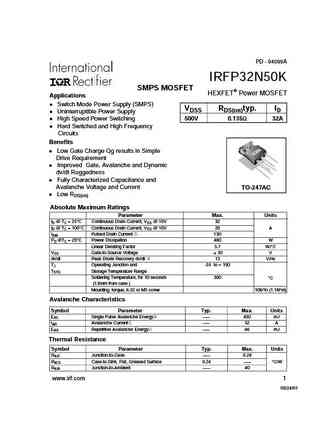
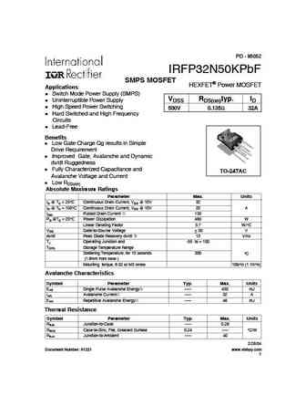
PD - 94099A IRFP32N50K SMPS MOSFET HEXFET Power MOSFET Applications Switch Mode Power Supply (SMPS) VDSS RDS(on)typ. ID Uninterruptible Power Supply High Speed Power Switching 500V 0.135 32A Hard Switched and High Frequency Circuits Benefits Low Gate Charge Qg results in Simple Drive Requirement Improved Gate, Avalanche and Dynamic dv/dt Ruggedness Fully Characterize
irfp22n50apbf.pdf
PD - 95004 IRFP22N50APbF SMPS MOSFET HEXFET Power MOSFET Applications VDSS RDS(on) max ID l Switch Mode Power Supply (SMPS) l UninterruptIble Power Supply 500V 0.23 22A l High Speed Power Switching l Lead-Free Benefits l Low Gate Charge Qg results in Simple Drive Requirement l Improved Gate, Avalanche and Dynamic dv/dt Ruggedness l Fully Characterized Capacitance and Avalan
irfba22n50a.pdf
PD-91866B IRFBA22N50A SMPS MOSFET HEXFET Power MOSFET Applications VDSS RDS(on) max ID Switch Mode Power Supply ( SMPS ) Uninterruptible Power Supply 500V 0.23 24A High Speed Power Switching Benefits Low Gate Charge Qg results in Simple Drive Requirement Improved Gate, Avalanche and Dynamic dv/dt Ruggedness Fully Characterized Capacitance and Avalanche Voltage and Curr
irfbl12n50a.pdf
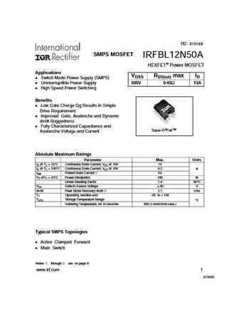
PD - 91818A SMPS MOSFET IRFBL12N50A HEXFET Power MOSFET Applications VDSS RDS(on) max ID Switch Mode Power Supply (SMPS) Uninterruptible Power Supply 500V 0.45 13A High Speed Power Switching Benefits Low Gate Charge Qg Results in Simple Drive Requirement Improved Gate, Avalanche and Dynamic dv/dt Ruggedness Fully Characterized Capacitance and Super-D2PakTM Avalanche V
phu2n50e 1.pdf
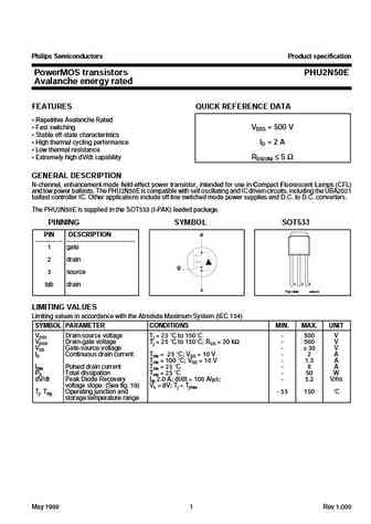
Philips Semiconductors Product specification PowerMOS transistors PHU2N50E Avalanche energy rated FEATURES QUICK REFERENCE DATA Repetitive Avalanche Rated Fast switching VDSS = 500 V Stable off-state characteristics High thermal cycling performance ID = 2 A Low thermal resistance Extremely high dV/dt capability RDS(ON) 5 GENERAL DESCRIPTION N-channe
2n5087 cnv 2.pdf

DISCRETE SEMICONDUCTORS DATA SHEET book, halfpage M3D186 2N5087 PNP general purpose transistor Product specification 1997 Jul 02 Supersedes data of September 1994 File under Discrete Semiconductors, SC04 Philips Semiconductors Product specification PNP general purpose transistor 2N5087 FEATURES PINNING Low current (max. 100 mA) PIN DESCRIPTION Low voltage (max. 50 V). 1
phx2n50e.pdf
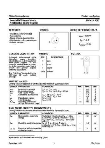
Philips Semiconductors Product specification PowerMOS transistors PHX2N50E Avalanche energy rated FEATURES SYMBOL QUICK REFERENCE DATA d Repetitive Avalanche Rated Fast switching VDSS = 500 V Stable off-state characteristics High thermal cycling performance ID = 1.4 A g Isolated package RDS(ON) 5 s GENERAL DESCRIPTION PINNING SOT186A N-channel, enhan
phb2n50 1.pdf
Philips Semiconductors Product specification PowerMOS transistor PHB2N50 GENERAL DESCRIPTION QUICK REFERENCE DATA N-channel enhancement mode SYMBOL PARAMETER MAX. UNIT field-effect power transistor in a plastic envelope suitable for surface VDS Drain-source voltage 500 V mounting featuring high avalanche ID Drain current (DC) 2 A energy capability, stable off-state Ptot Total power dis
2n5088 3.pdf
DISCRETE SEMICONDUCTORS DATA SHEET book, halfpage M3D186 2N5088 NPN general purpose transistor 1997 Sep 03 Product specification Supersedes data of 1997 Jul 03 File under Discrete Semiconductors, SC04 Philips Semiconductors Product specification NPN general purpose transistor 2N5088 FEATURES PINNING Low current (max. 100 mA) PIN DESCRIPTION Low voltage (max. 30 V). 1 co
php2n50e 3.pdf
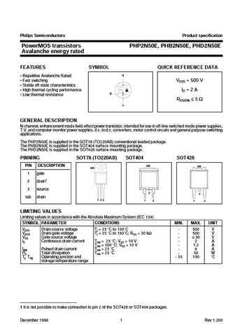
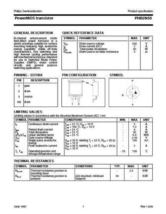
Philips Semiconductors Product specification PowerMOS transistors PHP2N50E, PHB2N50E, PHD2N50E Avalanche energy rated FEATURES SYMBOL QUICK REFERENCE DATA d Repetitive Avalanche Rated Fast switching VDSS = 500 V Stable off-state characteristics High thermal cycling performance ID = 2 A g Low thermal resistance RDS(ON) 5 s GENERAL DESCRIPTION N-channe
php2n50e phb2n50e phd2n50e.pdf

Philips Semiconductors Product specification PowerMOS transistors PHP2N50E, PHB2N50E, PHD2N50E Avalanche energy rated FEATURES SYMBOL QUICK REFERENCE DATA d Repetitive Avalanche Rated Fast switching VDSS = 500 V Stable off-state characteristics High thermal cycling performance ID = 2 A g Low thermal resistance RDS(ON) 5 s GENERAL DESCRIPTION N-channe
php2n50 1.pdf
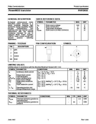
Philips Semiconductors Product specification PowerMOS transistor PHP2N50 GENERAL DESCRIPTION QUICK REFERENCE DATA N-channel enhancement mode SYMBOL PARAMETER MAX. UNIT field-effect power transistor in a plastic envelope featuring high VDS Drain-source voltage 500 V avalanche energy capability, stable ID Drain current (DC) 2 A off-state characteristics, fast Ptot Total power dissipation
stf12n50u.pdf

STF12N50U N-channel 500 V, 0.55 , 10 A TO-220FP Ultrafast MESH Power MOSFET Features RDS(on) Type VDSS ID Pw max STF12N50U 500 V
stf12n50m2.pdf
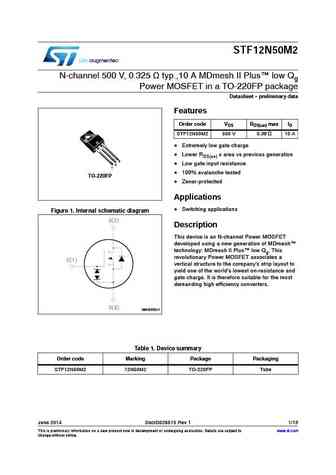
STF12N50M2 N-channel 500 V, 0.325 typ.,10 A MDmesh II Plus low Qg Power MOSFET in a TO-220FP package Datasheet - preliminary data Features Order code VDS RDS(on) max ID STF12N50M2 500 V 0.38 10 A Extremely low gate charge Lower RDS(on) x area vs previous generation 3 2 Low gate input resistance 1 100% avalanche tested TO-220FP Zener-protected Appli
stp12n50m2.pdf
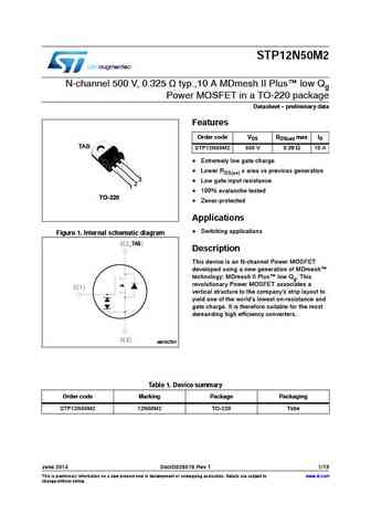
STP12N50M2 N-channel 500 V, 0.325 typ.,10 A MDmesh II Plus low Qg Power MOSFET in a TO-220 package Datasheet - preliminary data Features Order code VDS RDS(on) max ID TAB STP12N50M2 500 V 0.38 10 A Extremely low gate charge Lower RDS(on) x area vs previous generation 3 Low gate input resistance 2 1 100% avalanche tested TO-220 Zener-protected Appl
std2n50.pdf

STD2N50 N - CHANNEL ENHANCEMENT MODE POWER MOS TRANSISTOR TYPE V R I DSS DS(on) D STD2N50 500 V
std12n50m2.pdf
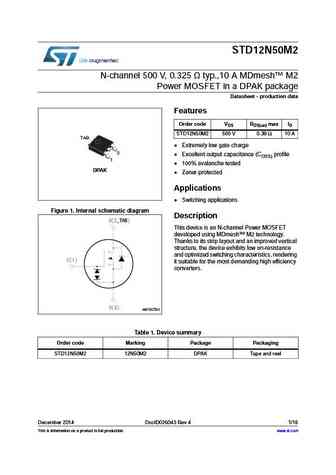
STD12N50M2 N-channel 500 V, 0.325 typ.,10 A MDmesh M2 Power MOSFET in a DPAK package Datasheet - production data Features Order code VDS RDS(on) max ID STD12N50M2 500 V 0.38 10 A TAB Extremely low gate charge 3 Excellent output capacitance (COSS) profile 1 100% avalanche tested DPAK Zener-protected Applications Switching applications Figure 1. Int
2n5038.pdf
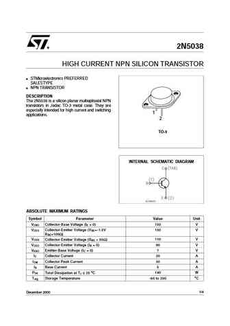
2N5038 HIGH CURRENT NPN SILICON TRANSISTOR STMicroelectronics PREFERRED SALESTYPE NPN TRANSISTOR DESCRIPTION The 2N5038 is a silicon planar multiepitaxial NPN transistors in Jedec TO-3 metal case. They are especially intended for high current and switching 1 applications. 2 TO-3 INTERNAL SCHEMATIC DIAGRAM ABSOLUTE MAXIMUM RATINGS Symbol Parameter Value Unit VCBO Collect
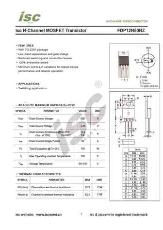
fdp12n50nz fdpf12n50nz.pdf
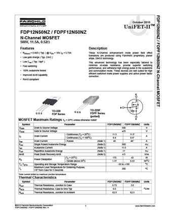
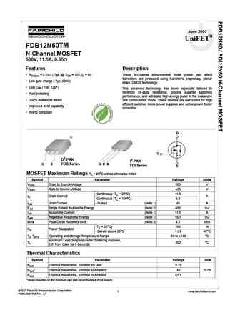
October 2010 UniFET-IITM FDP12N50NZ / FDPF12N50NZ N-Channel MOSFET 500V, 11.5A, 0.52 Features Description RDS(on) = 0.46 ( Typ. ) @ VGS = 10V, ID = 5.75A These N-Channel enhancement mode power field effect transistors are produced using Fairchild s proprietary, planar Low gate charge ( Typ. 23nC ) stripe, DMOS technology. Low Crss ( Typ. 14pF ) This advanced tech
fqb12n50tm am002 fqi12n50tu.pdf
TM QFET FQB12N50 / FQI12N50 500V N-Channel MOSFET General Description Features These N-Channel enhancement mode power field effect 12.1A, 500V, RDS(on) = 0.49 @VGS = 10 V transistors are produced using Fairchild s proprietary, Low gate charge ( typical 39 nC) planar stripe, DMOS technology. Low Crss ( typical 25 pF) This advanced technology has been especially tailored
fqp2n50.pdf
April 2000 TM QFET QFET QFET QFET 500V N-ChanneI MOSFET GeneraI Description Features These N-Channel enhancement mode power field effect 2.1A, 500V, RDS(on) = 5.3 @VGS = 10 V transistors are produced using Fairchild s proprietary, Low gate charge ( typical 6.0 nC) planar stripe, DMOS technology. Low Crss ( typical 4.0 pF) This advanced technology has been
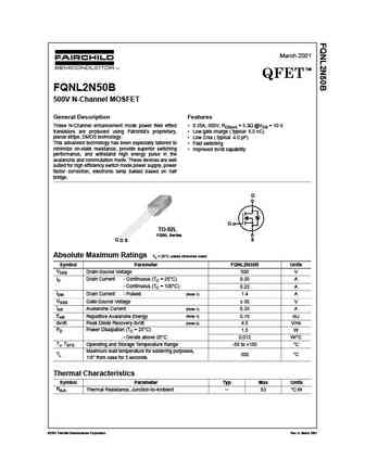
fqnl2n50b.pdf

March 2001 TM QFET FQNL2N50B 500V N-Channel MOSFET General Description Features These N-Channel enhancement mode power field effect 0.35A, 500V, RDS(on) = 5.3 @VGS = 10 V transistors are produced using Fairchild s proprietary, Low gate charge ( typical 6.0 nC) planar stripe, DMOS technology. Low Crss ( typical 4.0 pF) This advanced technology has been especially tailo
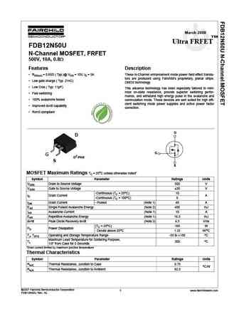
fdb12n50f.pdf
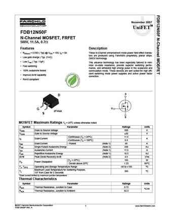
November 2007 UniFETTM FDB12N50F tm N-Channel MOSFET, FRFET 500V, 11.5A, 0.7 Features Description RDS(on) = 0.59 ( Typ.)@ VGS = 10V, ID = 6A These N-Channel enhancement mode power field effect transis- tors are produced using Fairchild s proprietary, planar stripe, Low gate charge ( Typ. 21nC) DMOS technology. Low Crss ( Typ. 11pF) This advance technology has b
fdp12n50 fdpf12n50.pdf
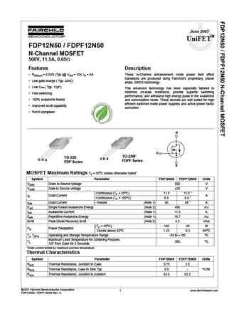
June 2007 UniFETTM FDP12N50 / FDPF12N50 tm N-Channel MOSFET 500V, 11.5A, 0.65 Features Description RDS(on) = 0.55 (Typ.)@ VGS = 10V, ID = 6A These N-Channel enhancement mode power field effect transistors are produced using Fairchild s proprietary, planar Low gate charge ( Typ. 22nC) stripe, DMOS technology. Low Crss ( Typ. 11pF) This advanced technology has be
fqu2n50b.pdf
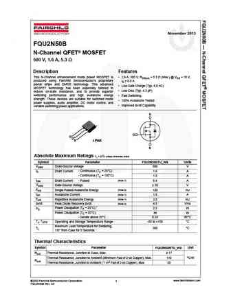
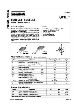
November 2013 FQU2N50B N-Channel QFET MOSFET 500 V, 1.6 A, 5.3 Description Features This N-Channel enhancement mode power MOSFET is 1.6 A, 500 V, RDS(on) = 5.3 (Max.) @ VGS = 10 V, produced using Fairchild Semiconductor s proprietary ID = 0.8 A planar stripe and DMOS technology. This advanced Low Gate Charge (Typ. 6.0 nC) MOSFET technology has been especially tailo
fqnl2n50bbu fqnl2n50bta.pdf
March 2001 TM QFET FQNL2N50B 500V N-Channel MOSFET General Description Features These N-Channel enhancement mode power field effect 0.35A, 500V, RDS(on) = 5.3 @VGS = 10 V transistors are produced using Fairchild s proprietary, Low gate charge ( typical 6.0 nC) planar stripe, DMOS technology. Low Crss ( typical 4.0 pF) This advanced technology has been especially tailo
fdb12n50tm.pdf
June 2007 UniFETTM FDB12N50TM tm N-Channel MOSFET 500V, 11.5A, 0.65 Features Description RDS(on) = 0.55 ( Typ.)@ VGS = 10V, ID = 6A These N-Channel enhancement mode power field effect transistors are produced using Fairchild s proprietary, planar Low gate charge ( Typ. 22nC) stripe, DMOS technology. Low Crss ( Typ. 12pF) This advanced technology has been especi
2n5086 2n5087 mmbt5087.pdf

2N5086/2N5087/MMBT5087 PNP General Purpose Amplifier 3 This device is designed for low level, high gain, low noise general purpose amplifier applications at collector currents to 50mA. 2 SOT-23 TO-92 1 Mark 2Q 1 1. Emitter 2. Base 3. Collector 1. Base 2. Emitter 3. Collector Absolute Maximum Ratings* Ta=25 C unless otherwise noted Symbol Parameter Value Units VCEO Collect
fqb2n50tm.pdf
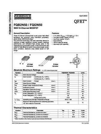
April 2000 TM QFET QFET QFET QFET FQB2N50 / FQI2N50 500V N-ChanneI MOSFET GeneraI Description Features These N-Channel enhancement mode power field effect 2.1A, 500V, RDS(on) = 5.3 @VGS = 10 V transistors are produced using Fairchild s proprietary, Low gate charge ( typical 6.0 nC) planar stripe, DMOS technology. Low Crss ( typical 4.0 pF) This advanced technolog
fqd2n50tf fqd2n50tm.pdf
April 2000 TM QFET QFET QFET QFET FQD2N50 / FQU2N50 500V N-ChanneI MOSFET GeneraI Description Features These N-Channel enhancement mode power field effect 1.6A, 500V, RDS(on) = 5.3 @VGS = 10 V transistors are produced using Fairchild s proprietary, Low gate charge ( typical 6.0 nC) planar stripe, DMOS technology. Low Crss ( typical 4.0 pF) This advanced technolog
fdp12n50f fdpf12n50ft.pdf
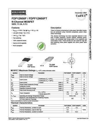
December 2007 UniFETTM FDP12N50F / FDPF12N50FT tm N-Channel MOSFET 500V, 11.5A, 0.7 Features Description RDS(on) = 0.59 ( Typ.)@ VGS = 10V, ID = 6A These N-Channel enhancement mode power field effect transis- tors are produced using Fairchild s proprietary, planar stripe, Low gate charge ( Typ. 21nC) DMOS technology. Low Crss ( Typ. 11pF) This advance technolog
fqu2n50btu.pdf
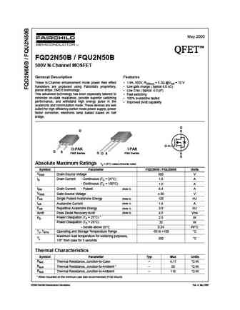
May 2000 TM QFET QFET QFET QFET FQD2N50B / FQU2N50B 500V N-Channel MOSFET General Description Features These N-Channel enhancement mode power field effect 1.6A, 500V, RDS(on) = 5.3 @VGS = 10 V transistors are produced using Fairchild s proprietary, Low gate charge ( typical 6.0 nC) planar stripe, DMOS technology. Low Crss ( typical 4.0 pF) This advanced technology
fdp12n50u fdpf12n50ut.pdf
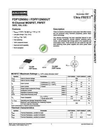
November 2007 Ultra FRFETTM FDP12N50U / FDPF12N50UT tm N-Channel MOSFET, FRFET 500V, 10A, 0.8 Features Description RDS(on) = 0.65 ( Typ.)@ VGS = 10V, ID = 5A These N-Channel enhancement mode power field effect transis- tors are produced using Fairchild s proprietary, planar stripe, Low gate charge ( Typ. 21nC) DMOS technology. Low Crss ( Typ. 11pF) This advance
fdb12n50u.pdf
March 2008 TM Ultra FRFET FDB12N50U tm N-Channel MOSFET, FRFET 500V, 10A, 0.8 Features Description RDS(on) = 0.65 ( Typ.)@ VGS = 10V, ID = 5A These N-Channel enhancement mode power field effect transis- tors are produced using Fairchild s proprietary, planar stripe, Low gate charge ( Typ. 21nC) DMOS technology. Low Crss ( Typ. 11pF) This advance technology has
fdp22n50n.pdf
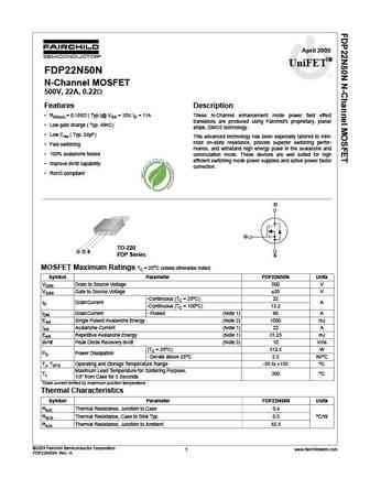
April 2009 UniFETTM FDP22N50N N-Channel MOSFET 500V, 22A, 0.22 Features Description RDS(on) = 0.185 ( Typ.)@ VGS = 10V, ID = 11A These N-Channel enhancement mode power field effect transistors are produced using Fairchild s proprietary, planar Low gate charge ( Typ. 49nC) stripe, DMOS technology. Low Crss ( Typ. 24pF) This advanced technology has been especiall
fdpf12n50nzt.pdf

October 2010 UniFET-IITM FDP12N50NZ / FDPF12N50NZ N-Channel MOSFET 500V, 11.5A, 0.52 Features Description RDS(on) = 0.46 ( Typ. ) @ VGS = 10V, ID = 5.75A These N-Channel enhancement mode power field effect transistors are produced using Fairchild s proprietary, planar Low gate charge ( Typ. 23nC ) stripe, DMOS technology. Low Crss ( Typ. 14pF ) This advanced tech
fdp12n50 fdpf12n50t.pdf
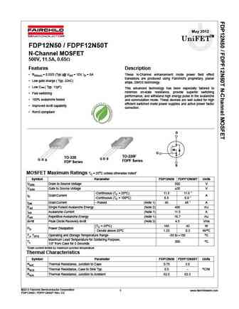
May 2012 UniFETTM FDP12N50 / FDPF12N50T tm N-Channel MOSFET 500V, 11.5A, 0.65 Features Description RDS(on) = 0.55 (Typ.)@ VGS = 10V, ID = 6A These N-Channel enhancement mode power field effect transistors are produced using Fairchild s proprietary, planar Low gate charge ( Typ. 22nC) stripe, DMOS technology. Low Crss ( Typ. 11pF) This advanced technology has be
2n5088 mmbt5088 2n5089 mmbt5089.pdf

2N5088 MMBT5088 2N5089 MMBT5089 C E C TO-92 B B SOT-23 E Mark 1Q / 1R NPN General Purpose Amplifier This device is designed for low noise, high gain, general purpose amplifier applications at collector currents from 1 A to 50 mA. Absolute Maximum Ratings* TA = 25 C unless otherwise noted Symbol Parameter Value Units VCEO Collector-Emitter Voltage 2N5088 30 V 2N5089 25 V VCBO
fqpf2n50.pdf
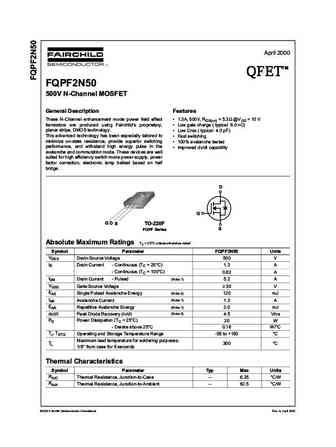
April 2000 TM QFET QFET QFET QFET 500V N-ChanneI MOSFET GeneraI Description Features These N-Channel enhancement mode power field effect 1.3A, 500V, RDS(on) = 5.3 @VGS = 10 V transistors are produced using Fairchild s proprietary, Low gate charge ( typical 6.0 nC) planar stripe, DMOS technology. Low Crss ( typical 4.0 pF) This advanced technology has bee
2n5088-2n5089.pdf
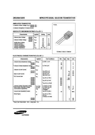
2N5088/5089 NPN EPITAXIAL SILICON TRANSISTOR AMPLIFIER TRANSISTOR TO-92 Collector-Emitter Voltage VCEO= 2N5088 30V 2N5089 25V Collector Dissipation PC (max)=625mW ABSOLUTE MAXIMUM RATINGS (T =25 ) A Characteristic Symbol Rating Unit Collector-Base Voltage 2N5088 VCBO 2N5089 30 V Collector-Emitter Voltage 2N5088 VCEO 30 V 2N5089 25 V Emitter-Base Voltage VEBO 4.5 V
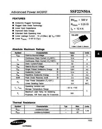
ssh22n50a.pdf
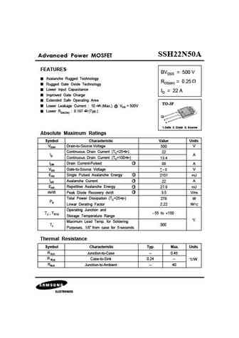
SSH22N50A Advanced Power MOSFET FEATURES BVDSS = 500 V Avalanche Rugged Technology RDS(on) = 0.25 Rugged Gate Oxide Technology Lower Input Capacitance ID = 22 A Improved Gate Charge Extended Safe Operating Area TO-3P Lower Leakage Current 10 A (Max.) @ VDS = 500V Lower RDS(ON) 0.197 (Typ.) 1 2 3 1.Gate 2. Drain 3. Source Absolute Maximum Ratings Symbol C
rdd022n50.pdf
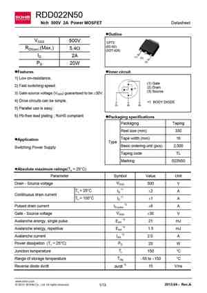
RDD022N50 Nch 500V 2A Power MOSFET Datasheet lOutline VDSS 500V CPT3 (SC-63) RDS(on) (Max.) 5.4W (SOT-428) ID 2A (1) (2) (3) PD 20W lFeatures lInner circuit 1) Low on-resistance. (1) Gate 2) Fast switching speed. (2) Drain (3) Source 3) Gate-source voltage (VGSS) guaranteed to be 30V. 4) Drive circuits can be simple. *1 BODY DIODE 5) Parallel use is easy.
sihg32n50d.pdf
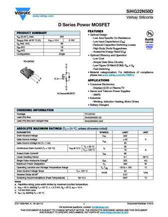
SiHG32N50D www.vishay.com Vishay Siliconix D Series Power MOSFET FEATURES PRODUCT SUMMARY Optimal Design VDS (V) at TJ max. 550 - Low Area Specific On-Resistance RDS(on) max. at 25 C ( ) VGS = 10 V 0.150 - Low Input Capacitance (Ciss) Qg max. (nC) 96 - Reduced Capacitive Switching Losses Qgs (nC) 18 - High Body Diode Ruggedness Qgd (nC) 29 - Avalanche Energy Rated (UIS)
irfp22n50a sihfp22n50a.pdf
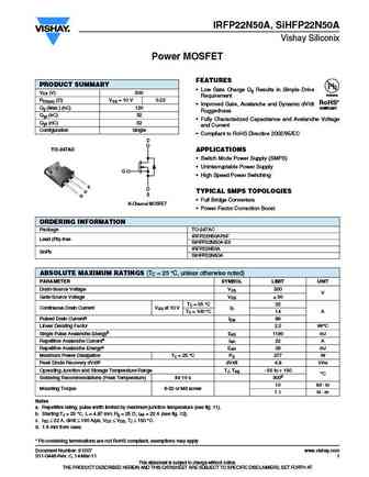
IRFP22N50A, SiHFP22N50A Vishay Siliconix Power MOSFET FEATURES PRODUCT SUMMARY Low Gate Charge Qg Results in Simple Drive VDS (V) 500 Available Requirement RDS(on) ( )VGS = 10 V 0.23 RoHS* Improved Gate, Avalanche and Dynamic dV/dt Qg (Max.) (nC) 120 COMPLIANT Ruggedness Qgs (nC) 32 Fully Characterized Capacitance and Avalanche Voltage Qgd (nC) 52 and Current Con
sihg22n50d.pdf

SiHG22N50D www.vishay.com Vishay Siliconix D Series Power MOSFET FEATURES PRODUCT SUMMARY Optimal Design VDS (V) at TJ max. 550 - Low Area Specific On-Resistance RDS(on) max. at 25 C ( ) VGS = 10 V 0.230 - Low Input Capacitance (Ciss) Qg max. (nC) 98 - Reduced Capacitive Switching Losses Qgs (nC) 13 - High Body Diode Ruggedness Qgd (nC) 22 - Avalanche Energy Rated (UIS)
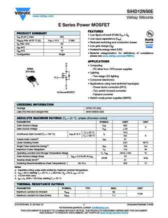
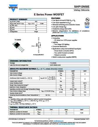
irfp32n50k irfp32n50kpbf sihfp32n50k.pdf

IRFP32N50K, SiHFP32N50K Vishay Siliconix Power MOSFET FEATURES PRODUCT SUMMARY Low Gate Charge Qg Results in Simple Drive VDS (V) 500 Available Requirement RDS(on) ( )VGS = 10 V 0.135 RoHS* Improved Gate, Avalanche and Dynamic dV/dt Qg (Max.) (nC) 190 COMPLIANT Ruggedness Qgs (nC) 59 Fully Characterized Capacitance and Avalanche Voltage Qgd (nC) 84 and Current Con
sihb12n50e.pdf
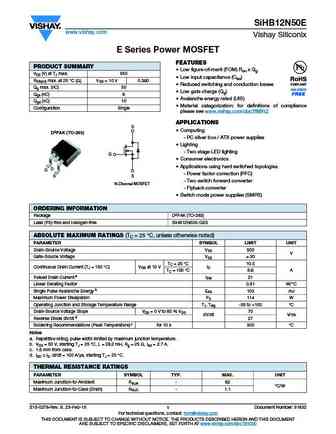
SiHB12N50E www.vishay.com Vishay Siliconix E Series Power MOSFET FEATURES PRODUCT SUMMARY Low figure-of-merit (FOM) Ron x Qg VDS (V) at TJ max. 550 Low input capacitance (Ciss) RDS(on) max. at 25 C ( ) VGS = 10 V 0.380 Reduced switching and conduction losses Qg max. (nC) 50 Low gate charge (Qg) Qgs (nC) 6 Avalanche energy rated (UIS) Qgd (nC) 10 Materi
sihd12n50e.pdf
SiHD12N50E www.vishay.com Vishay Siliconix E Series Power MOSFET FEATURES PRODUCT SUMMARY Low figure-of-merit (FOM) Ron x Qg VDS (V) at TJ max. 550 Low input capacitance (Ciss) RDS(on) max. at 25 C ( ) VGS = 10 V 0.380 Reduced switching and conduction losses Qg max. (nC) 50 Low gate charge (Qg) Qgs (nC) 6 Avalanche energy rated (UIS) Qgd (nC) 10 Materi
irfp32n50k sihfp32n50k.pdf
IRFP32N50K, SiHFP32N50K Vishay Siliconix Power MOSFET FEATURES PRODUCT SUMMARY Low Gate Charge Qg Results in Simple Drive VDS (V) 500 Available Requirement RDS(on) ( )VGS = 10 V 0.135 RoHS* Improved Gate, Avalanche and Dynamic dV/dt Qg (Max.) (nC) 190 COMPLIANT Ruggedness Qgs (nC) 59 Fully Characterized Capacitance and Avalanche Voltage Qgd (nC) 84 and Current Con
sihp12n50c sihb12n50c sihf12n50c.pdf

SiHP12N50C, SiHB12N50C, SiHF12N50C Vishay Siliconix Power MOSFET FEATURES PRODUCT SUMMARY Low Figure-of-Merit Ron x Qg VDS (V) at TJ max. 560 V RDS(on) ( )VGS = 10 V 0.555 100 % Avalanche Tested Qg (Max.) (nC) 48 Gate Charge Improved Qgs (nC) 12 Trr/Qrr Improved Qgd (nC) 15 Configuration Single Compliant to RoHS Directive 2002/95/EC TO-220AB TO-220 FULLPAK
sihp12n50e.pdf
SiHP12N50E www.vishay.com Vishay Siliconix E Series Power MOSFET FEATURES PRODUCT SUMMARY Low figure-of-merit (FOM) Ron x Qg VDS (V) at TJ max. 550 Low input capacitance (Ciss) RDS(on) max. at 25 C ( ) VGS = 10 V 0.380 Reduced switching and conduction losses Qg max. (nC) 50 Low gate charge (Qg) Qgs (nC) 6 Avalanche energy rated (UIS) Qgd (nC) 10 Materi
sihb12n50c sihf12n50c sihp12n50c.pdf
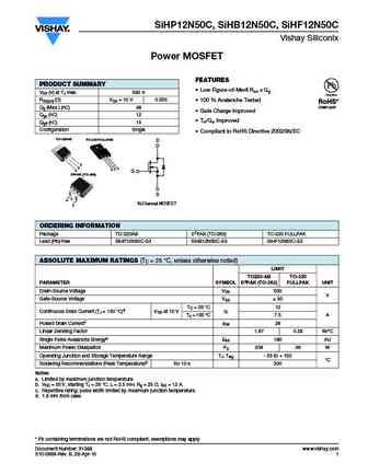
SiHP12N50C, SiHB12N50C, SiHF12N50C Vishay Siliconix Power MOSFET FEATURES PRODUCT SUMMARY Low Figure-of-Merit Ron x Qg VDS (V) at TJ max. 560 V RDS(on) ( )VGS = 10 V 0.555 100 % Avalanche Tested Qg (Max.) (nC) 48 Gate Charge Improved Qgs (nC) 12 Trr/Qrr Improved Qgd (nC) 15 Configuration Single Compliant to RoHS Directive 2002/95/EC TO-220AB TO-220 FULLPAK
siha12n50e.pdf
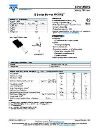
SiHA12N50E www.vishay.com Vishay Siliconix E Series Power MOSFET FEATURES PRODUCT SUMMARY Low figure-of-merit (FOM) Ron x Qg VDS (V) at TJ max. 550 Low input capacitance (Ciss) RDS(on) max. at 25 C ( ) VGS = 10 V 0.380 Reduced switching and conduction losses Qg max. (nC) 50 Low gate charge (Qg) Qgs (nC) 6 Avalanche energy rated (UIS) Qgd (nC) 10 Materi
irfp22n50apbf sihfp22n50a.pdf

IRFP22N50A, SiHFP22N50A Vishay Siliconix Power MOSFET FEATURES PRODUCT SUMMARY Low Gate Charge Qg Results in Simple Drive VDS (V) 500 Available Requirement RDS(on) ( )VGS = 10 V 0.23 RoHS* Improved Gate, Avalanche and Dynamic dV/dt Qg (Max.) (nC) 120 COMPLIANT Ruggedness Qgs (nC) 32 Fully Characterized Capacitance and Avalanche Voltage Qgd (nC) 52 and Current Con
2n5022 2n5023.pdf
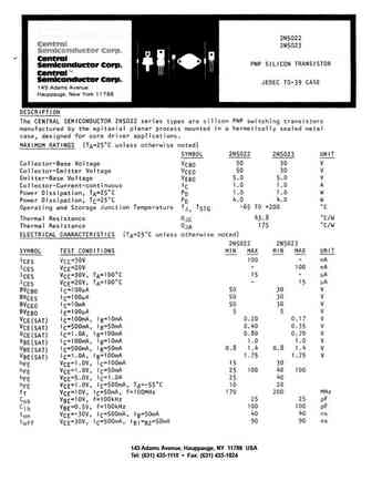
145 Adams Avenue, Hauppauge, NY 11788 USA Tel (631) 435-1110 Fax (631) 435-1824
2n5086 2n5087.pdf
145 Adams Avenue, Hauppauge, NY 11788 USA Tel (631) 435-1110 Fax (631) 435-1824
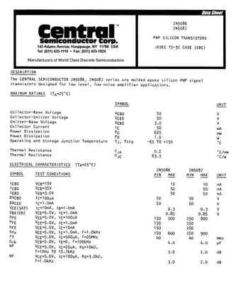
2n5058 2n5059.pdf
145 Adams Avenue, Hauppauge, NY 11788 USA Tel (631) 435-1110 Fax (631) 435-1824
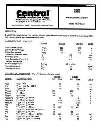
2n5088 2n5089.pdf
145 Adams Avenue, Hauppauge, NY 11788 USA Tel (631) 435-1110 Fax (631) 435-1824
zxt12n50dx.pdf
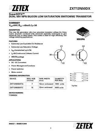
ZXT12N50DX SuperSOT4 DUAL 50V NPN SILICON LOW SATURATION SWITCHING TRANSISTOR SUMMARY VCEO=50V; RSAT = 45m ; IC= 3A DESCRIPTION This new 4th generation ultra low saturation transistor utilises the Zetex matrix structure combined with advanced assembly techniques to give extremely low on state losses. This makes it ideal for high efficiency, low voltage switching applications. MSOP8
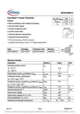
spw52n50c3.pdf
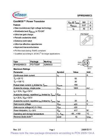
SPW52N50C3 CoolMOS Power Transistor VDS @ Tjmax 560 V Feature RDS(on) 0.07 New revolutionary high voltage technology ID 52 A Worldwide best RDS(on) in TO-247 PG-TO247 Ultra low gate charge Periodic avalanche rated Extreme dv/dt rated Ultra low effective capacitances Improved transconductance Type Package Marking SPW52N50C3 PG-TO247 52N50C3 Maxim
spw32n50c3.pdf
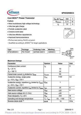
SPW32N50C3 Cool MOS Power Transistor VDS @ Tjmax 560 V Feature RDS(on) 0.11 New revolutionary high voltage technology ID 32 A Ultra low gate charge PG-TO247 Periodic avalanche rated Extreme dv/dt rated Ultra low effective capacitances Improved transconductance Type Package Ordering Code Marking SPW32N50C3 PG-TO247 Q67040-S4613 32N50C3 Maximum Rating
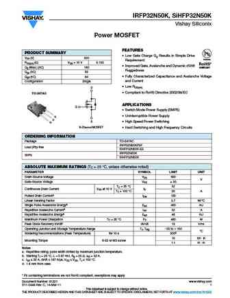
irfp22n50apbf.pdf

IRFP22N50APbF HEXFET Power MOSFET Applications D V 500V DSS Switch Mode Power Supply ( SMPS ) Uninterruptable Power Supply R DS(on) max 0.23 G High speed power switching I 22A D (Silicon Limited) S D Benefits Low Gate Charge Qg results in Simple Drive Requirement Improved Gate, Avalanche and dynamic dv/dt Ruggedness S Fully
spb12n50c3.pdf
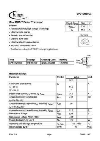
SPB12N50C3 Cool MOS Power Transistor VDS @ Tjmax 560 V Feature RDS(on) 0.38 New revolutionary high voltage technology ID 11.6 A Ultra low gate charge PG-TO263 Periodic avalanche rated Extreme dv/dt rated Ultra low effective capacitances Improved transconductance - Type Package Ordering Code Marking 12N50C3 SPB12N50C3 PG-TO263 Q67040-S4641 Maximum
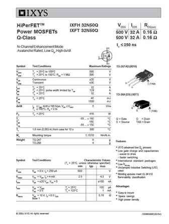
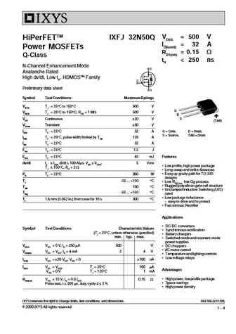
ixfh30n50 ixfh32n50 ixft30n50 ixft32n50.pdf
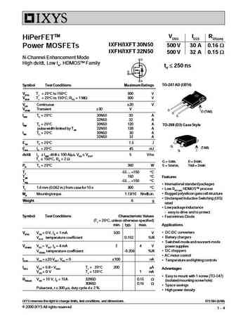
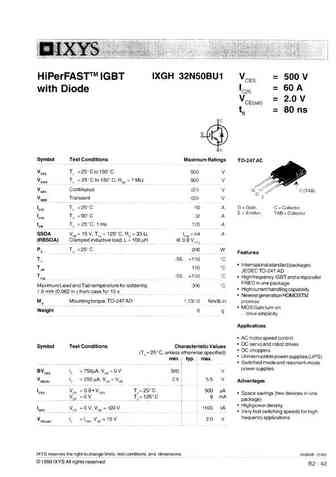
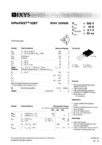
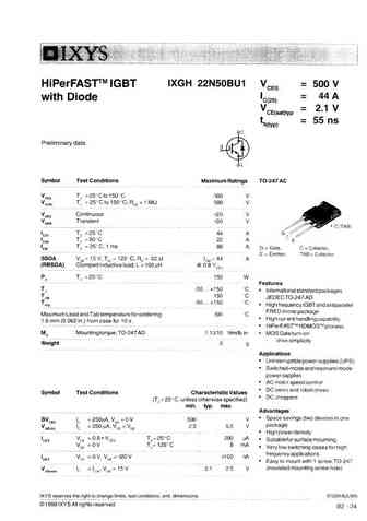
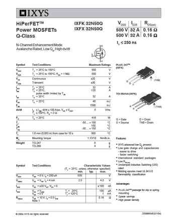
VDSS ID25 RDS(on) HiPerFETTM IXFH/IXFT 30N50 500 V 30 A 0.16 W Power MOSFETs IXFH/IXFT 32N50 500 V 32 A 0.15 W N-Channel Enhancement Mode High dv/dt, Low trr, HDMOSTM Family trr 250 ns TO-247 AD (IXFH) Symbol Test Conditions Maximum Ratings VDSS TJ = 25 C to 150 C 500 V VDGR TJ = 25 C to 150 C; RGS = 1 MW 500 V VGS Continuous 20 V VGSM Transient 30 V D (TAB) ID25 TC
ixfh42n50p2 ixft42n50p2.pdf
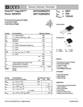
Advance Technical Information PolarP2TM HiperFETTM VDSS = 500V IXFH42N50P2 ID25 = 42A Power MOSFET IXFT42N50P2 RDS(on) 145m N-Channel Enhancement Mode Avalanche Rated Fast Intrinsic Diode TO-247 (IXFH) G D Symbol Test Conditions Maximum Ratings D (Tab) S VDSS TJ = 25 C to 150 C 500 V VDGR TJ = 25 C to 150 C, RGS = 1M 500 V TO-268 (IXF
ixfl132n50p3.pdf
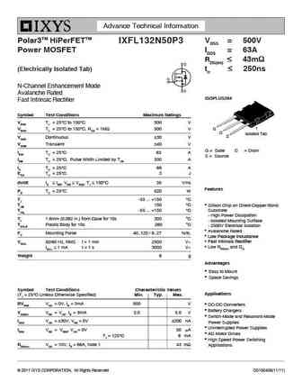
Advance Technical Information Polar3TM HiPerFETTM VDSS = 500V IXFL132N50P3 Power MOSFET ID25 = 63A RDS(on) 43m (Electrically Isolated Tab) trr 250ns N-Channel Enhancement Mode Avalanche Rated ISOPLUS264 Fast Intrinsic Rectifier Symbol Test Conditions Maximum Ratings VDSS TJ = 25 C to 150 C 500 V G VDGR TJ = 25 C to 15
ixth12n50a ixtm12n50a.pdf
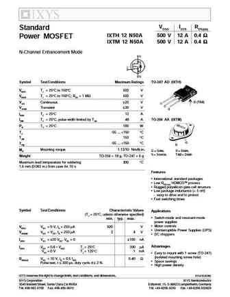
VDSS ID25 RDS(on) Standard IXTH 12 N50A 500 V 12 A 0.4 Power MOSFET IXTM 12 N50A 500 V 12 A 0.4 N-Channel Enhancement Mode Symbol Test Conditions Maximum Ratings TO-247 AD (IXTH) VDSS TJ = 25 C to 150 C 500 V VDGR TJ = 25 C to 150 C; RGS = 1 M 500 V D (TAB) VGS Continuous 20 V VGSM Transient 30 V ID25 TC = 25 C12 A IDM TC
mmix1f132n50p3.pdf
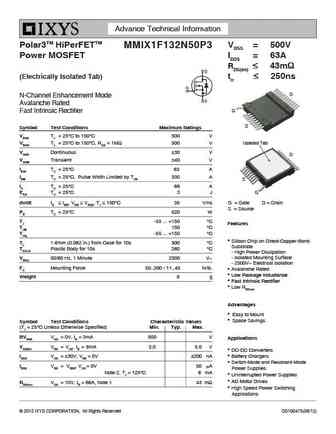
Advance Technical Information Polar3TM HiPerFETTM VDSS = 500V MMIX1F132N50P3 Power MOSFET ID25 = 63A RDS(on) 43m (Electrically Isolated Tab) trr 250ns D N-Channel Enhancement Mode Avalanche Rated G Fast Intrinsic Rectifier S Symbol Test Conditions Maximum Ratings VDSS TJ = 25 C to 150 C 500 V Isolated Tab VDGR TJ =
ixfh32n50q ixft32n50q.pdf
IXFH 32N50Q VDSS ID25 RDS(on) HiPerFETTM IXFT 32N50Q Power MOSFETs 500 V 32 A 0.16 500 V 32 A 0.16 Q-Class trr 250 ns N-Channel Enhancement Mode Avalanche Rated, Low Qg, High dv/dt Symbol Test Conditions Maximum Ratings TO-247 AD (IXFH) VDSS TJ = 25 C to 150 C 500 V VDGR TJ = 25 C to 150 C; RGS = 1 M 50
ixfk32n50q ixfx32n50q.pdf
VDSS ID25 RDS(on) IXFK 32N50Q HiPerFETTM IXFX 32N50Q 500 V 32 A 0.16 Power MOSFETs 500 V 32 A 0.16 Q-Class trr 250 ns N-Channel Enhancement Mode Avalanche Rated, Low Qg, High dv/dt Symbol Test Conditions Maximum Ratings PLUS 247TM (IXFX) VDSS TJ = 25 C to 150 C 500 V VDGR TJ = 25 C to 150 C; RGS = 1 M
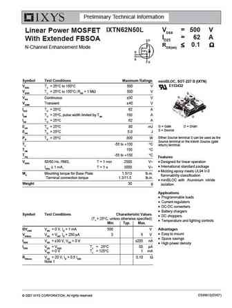
ixtb62n50l.pdf
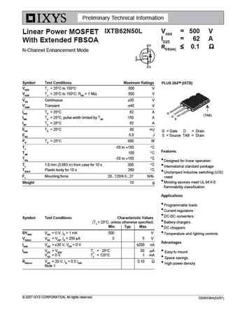
Preliminary Technical Information IXTB62N50L VDSS = 500 V Linear Power MOSFET ID25 = 62 A With Extended FBSOA RDS(on) 0.1 N-Channel Enhancement Mode Symbol Test Conditions Maximum Ratings PLUS 264TM (IXTB) VDSS TJ = 25 C to 150 C 500 V VDGR TJ = 25 C to 150 C; RGS = 1 M 500 V VGS Continuous 30 V VGSM Transient 40 V ID25 TC = 25 C 62
ixfj32n50q.pdf
VDSS = 500 V IXFJ 32N50Q HiPerFETTM ID(cont) = 32 A Power MOSFETs RDS(on) = 0.15 W Q-Class trr
ixtp02n50d ixtu02n50d ixty02n50d.pdf
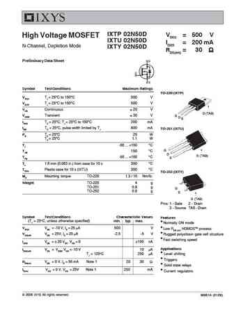
IXTP 02N50D VDSS = 500 V High Voltage MOSFET IXTU 02N50D ID25 = 200 mA N-Channel, Depletion Mode IXTY 02N50D RDS(on) = 30 Preliminary Data Sheet Symbol Test Conditions Maximum Ratings TO-220 (IXTP) VDSX TJ = 25 C to 150 C 500 V VDGX TJ = 25 C to 150 C 500 V VGS Continuous 20 V D (TAB) VGSM Transient 30 V G D S IDSS TC = 25 C; TJ = 25 C to 150 C
ixtn62n50l.pdf
Preliminary Technical Information IXTN62N50L VDSS = 500 V Linear Power MOSFET ID25 = 62 A With Extended FBSOA D RDS(on) 0.1 N-Channel Enhancement Mode G S S Symbol Test Conditions Maximum Ratings miniBLOC, SOT-227 B (IXTN) E153432 VDSS TJ = 25 C to 150 C 500 V VDGR TJ = 25 C to 150 C; RGS = 1 M 500 V S G VGS Continuous 30 V VGSM
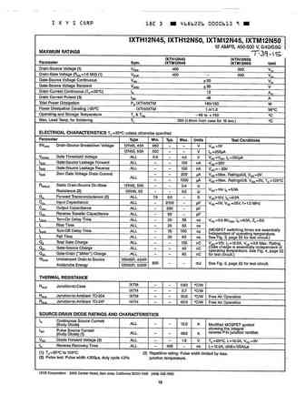
ixth22n50p ixtq22n50p ixtv22n50p.pdf
IXTH 22N50P VDSS = 500 V PolarHVTM IXTQ 22N50P ID25 = 22 A Power MOSFET IXTV 22N50P RDS(on) 270 m N-Channel Enhancement Mode IXTV 22N50PS Avalanche Rated TO-247 (IXTH) Symbol Test Conditions Maximum Ratings G (TAB) D VDSS TJ = 25 C to 150 C 500 V S VDGR TJ = 25 C to 150 C; RGS = 1 M 500 V VGS Continuous 30 V TO-3P (IXTQ) VGSM Trans
ixft52n50p2 ixfh52n50p2.pdf
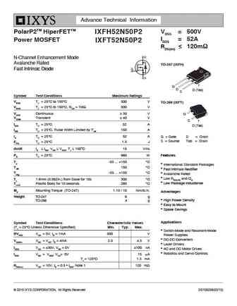
Advance Technical Information PolarP2TM HiperFETTM VDSS = 500V IXFH52N50P2 ID25 = 52A Power MOSFET IXFT52N50P2 RDS(on) 120m N-Channel Enhancement Mode Avalanche Rated TO-247 (IXFH) Fast Intrinsic Diode G D D (Tab) S Symbol Test Conditions Maximum Ratings VDSS TJ = 25 C to 150 C 500 V TO-268 (IXFT) VDGR TJ = 25 C to 150 C, RGS = 1M 50
ixfh22n50p ixfv22n50p.pdf
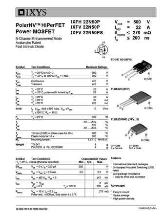
IXFH 22N50P VDSS = 500 V PolarHVTM HiPerFET IXFV 22N50P ID25 = 22 A Power MOSFET IXFV 22N50PS RDS(on) 270 m trr 200 ns N-Channel Enhancement Mode Avalanche Rated Fast Intrinsic Diode TO-247 AD (IXFH) Symbol Test Conditions Maximum Ratings VDSS TJ = 25 C to 150 C 500 V VDGR TJ = 25 C to 150 C; RGS = 1 M 500
ixti12n50p.pdf
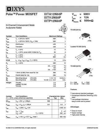
VDSS = 500V PolarTM Power MOSFET IXTA12N50P ID25 = 12A IXTI12N50P RDS(on) 500m IXTP12N50P N-Channel Enhancement Mode Avalanche Rated TO-263 (IXTA) Symbol Test Conditions Maximum Ratings G VDSS TJ = 25 C to 150 C 500 V S (TAB) VDGR TJ = 25 C to 150 C, RGS = 1M 500 V VGSS Continuous 30 V VGSM Transient 40 V Leaded TO-263 (IXTI) ID25
ixfr30n50q ixfr32n50q.pdf
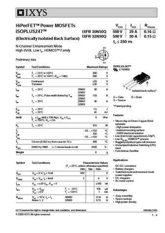
VDSS ID25 RDS(on) HiPerFETTM Power MOSFETs ISOPLUS247TM IXFR 30N50Q 500 V 29 A 0.16 W IXFR 32N50Q 500 V 30 A 0.15 W (Electrically Isolated Back Surface) trr 250 ns N-Channel Enhancement Mode High dV/dt, Low trr, HDMOSTM Family Preliminary data ISOPLUS 247TM Symbol Test Conditions Maximum Ratings E 153432 VDSS TJ = 25 C to 150 C 500 V VDGR TJ = 25 C to 150 C; RGS = 1 MW 500 V
2n5087rlrag.pdf

2N5087 Preferred Device Amplifier Transistor PNP Silicon Features Pb-Free Packages are Available* http //onsemi.com 3 COLLECTOR MAXIMUM RATINGS 2 BASE Rating Symbol Value Unit Collector-Emitter Voltage VCEO 50 Vdc 1 EMITTER Collector-Base Voltage VCBO 50 Vdc Emitter-Base Voltage VEBO 3.0 Vdc Collector Current - Continuous IC 50 mAdc TO-92 Total Device Dissipation @ TA = 2
fqnl2n50b.pdf

Is Now Part of To learn more about ON Semiconductor, please visit our website at www.onsemi.com Please note As part of the Fairchild Semiconductor integration, some of the Fairchild orderable part numbers will need to change in order to meet ON Semiconductor s system requirements. Since the ON Semiconductor product management systems do not have the ability to manage part nomenclatur
2n5088g.pdf

2N5088, 2N5089 Amplifier Transistors NPN Silicon Features http //onsemi.com Pb-Free Packages are Available* 3 COLLECTOR 2 MAXIMUM RATINGS BASE Rating Symbol Value Unit Collector - Emitter Voltage VCEO Vdc 1 EMITTER 2N5088 30 2N5089 25 Collector - Base Voltage VCBO Vdc 2N5088 35 TO-92 2N5089 30 CASE 29 Emitter - Base Voltage VEBO 3.0 Vdc STYLE 1 Collector Current - Conti
fdpf12n50ft.pdf

Is Now Part of To learn more about ON Semiconductor, please visit our website at www.onsemi.com Please note As part of the Fairchild Semiconductor integration, some of the Fairchild orderable part numbers will need to change in order to meet ON Semiconductor s system requirements. Since the ON Semiconductor product management systems do not have the ability to manage part nomenclatur
fdb12n50f.pdf
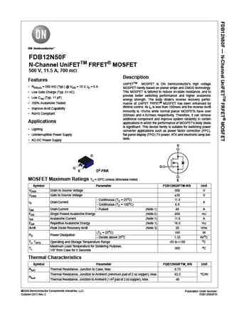
FDB12N50F N-Channel UniFETTM FRFET MOSFET 500 V, 11.5 A, 700 m Description Features UniFETTM MOSFET is ON Semiconductor s high voltage RDS(on) = 590 m (Typ.) @ VGS = 10 V, ID = 6 A MOSFET family based on planar stripe and DMOS technology. This MOSFET is tailored to reduce on-state resistance, and to Low Gate Charge (Typ. 21 nC) provide better switching performa
2n5087g.pdf
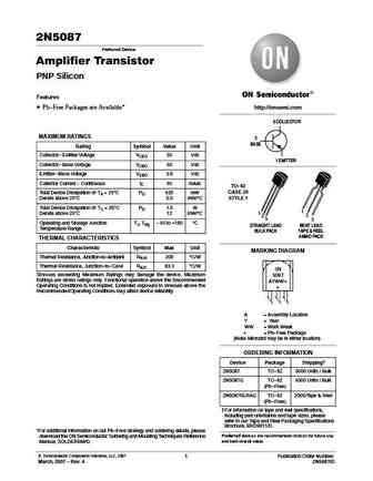
2N5087 Preferred Device Amplifier Transistor PNP Silicon Features Pb-Free Packages are Available* http //onsemi.com 3 COLLECTOR MAXIMUM RATINGS 2 BASE Rating Symbol Value Unit Collector-Emitter Voltage VCEO 50 Vdc 1 EMITTER Collector-Base Voltage VCBO 50 Vdc Emitter-Base Voltage VEBO 3.0 Vdc Collector Current - Continuous IC 50 mAdc TO-92 Total Device Dissipation @ TA = 2
fdpf12n50ut.pdf

Is Now Part of To learn more about ON Semiconductor, please visit our website at www.onsemi.com Please note As part of the Fairchild Semiconductor integration, some of the Fairchild orderable part numbers will need to change in order to meet ON Semiconductor s system requirements. Since the ON Semiconductor product management systems do not have the ability to manage part nomenclatur
2n5038g.pdf

2N5038 NPN Silicon Transistors Fast switching speeds and high current capacity ideally suit these parts for use in switching regulators, inverters, wide-band amplifiers and power oscillators in industrial and commercial applications. Features http //onsemi.com High Speed - tf = 0.5 ms (Max) High Current - IC(max) = 30 Amps 20 AMPERE Low Saturation - VCE(sat) = 2.5 V (Max)
fdb12n50tm.pdf

Is Now Part of To learn more about ON Semiconductor, please visit our website at www.onsemi.com Please note As part of the Fairchild Semiconductor integration, some of the Fairchild orderable part numbers will need to change in order to meet ON Semiconductor s system requirements. Since the ON Semiconductor product management systems do not have the ability to manage part nomenclatur
2n5060.pdf
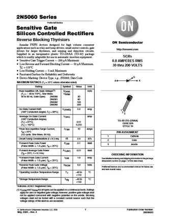
2N5060 Series Preferred Device Sensitive Gate Silicon Controlled Rectifiers Reverse Blocking Thyristors Annular PNPN devices designed for high volume consumer applications such as relay and lamp drivers, small motor controls, gate http //onsemi.com drivers for larger thyristors, and sensing and detection circuits. Supplied in an inexpensive plastic TO-226AA (TO-92) package SCRs which
2n5089g.pdf

2N5088, 2N5089 Amplifier Transistors NPN Silicon Features http //onsemi.com Pb-Free Packages are Available* 3 COLLECTOR 2 MAXIMUM RATINGS BASE Rating Symbol Value Unit Collector - Emitter Voltage VCEO Vdc 1 EMITTER 2N5088 30 2N5089 25 Collector - Base Voltage VCBO Vdc 2N5088 35 TO-92 2N5089 30 CASE 29 Emitter - Base Voltage VEBO 3.0 Vdc STYLE 1 Collector Current - Conti
2n5087-d.pdf

2N5087 Preferred Device Amplifier Transistor PNP Silicon Features Pb-Free Packages are Available* http //onsemi.com 3 COLLECTOR MAXIMUM RATINGS 2 BASE Rating Symbol Value Unit Collector-Emitter Voltage VCEO 50 Vdc 1 EMITTER Collector-Base Voltage VCBO 50 Vdc Emitter-Base Voltage VEBO 3.0 Vdc Collector Current - Continuous IC 50 mAdc TO-92 Total Device Dissipation @ TA = 2
fdp12n50 fdpf12n50t.pdf

Is Now Part of To learn more about ON Semiconductor, please visit our website at www.onsemi.com Please note As part of the Fairchild Semiconductor integration, some of the Fairchild orderable part numbers will need to change in order to meet ON Semiconductor s system requirements. Since the ON Semiconductor product management systems do not have the ability to manage part nomenclatur
2n5088 2n5089.pdf
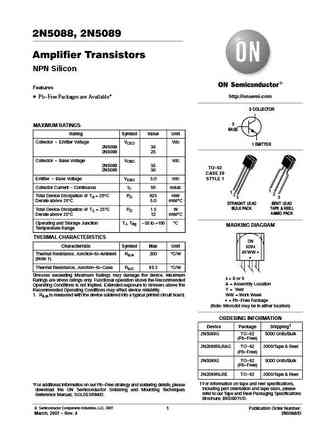
2N5088, 2N5089 Amplifier Transistors NPN Silicon Features http //onsemi.com Pb-Free Packages are Available* 3 COLLECTOR 2 MAXIMUM RATINGS BASE Rating Symbol Value Unit Collector - Emitter Voltage VCEO Vdc 1 EMITTER 2N5088 30 2N5089 25 Collector - Base Voltage VCBO Vdc 2N5088 35 TO-92 2N5089 30 CASE 29 Emitter - Base Voltage VEBO 3.0 Vdc STYLE 1 Collector Current - Conti
2n5038.pdf
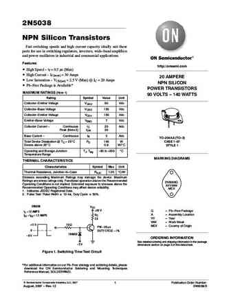
2N5038 NPN Silicon Transistors Fast switching speeds and high current capacity ideally suit these parts for use in switching regulators, inverters, wide-band amplifiers and power oscillators in industrial and commercial applications. Features http //onsemi.com High Speed - tf = 0.5 ms (Max) High Current - IC(max) = 30 Amps 20 AMPERE Low Saturation - VCE(sat) = 2.5 V (Max)
12n50.pdf
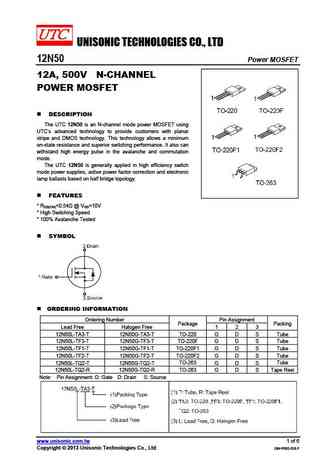
UNISONIC TECHNOLOGIES CO., LTD 12N50 Power MOSFET 12A, 500V N-CHANNEL POWER MOSFET DESCRIPTION The UTC 12N50 is an N-channel mode power MOSFET using UTC s advanced technology to provide customers with planar stripe and DMOS technology. This technology allows a minimum on-state resistance and superior switching performance. It also can withstand high energy pulse in the av
fmc12n50es.pdf
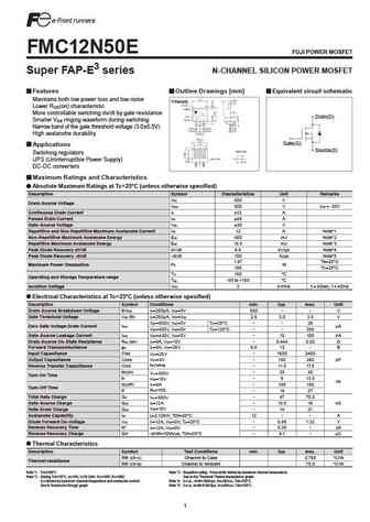
FMC12N50ES FUJI POWER MOSFET Super FAP-E3S series N-CHANNEL SILICON POWER MOSFET Features Outline Drawings [mm] Equivalent circuit schematic Maintains both low power loss and low noise T-Pack (S) Lower R (on) characteristic DS More controllable switching dv/dt by gate resistance Drain(D) Smaller V ringing waveform during switching GS Narrow band of the gate threshold voltage (3.7 0.
fmc12n50e.pdf
FMC12N50E FUJI POWER MOSFET Super FAP-E3 series N-CHANNEL SILICON POWER MOSFET Features Outline Drawings [mm] Equivalent circuit schematic Maintains both low power loss and low noise T-Pack(S) Lower R (on) characteristic DS More controllable switching dv/dt by gate resistance Drain(D) Smaller V ringing waveform during switching GS Narrow band of the gate threshold voltage (3.0 0.5V)
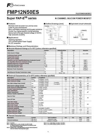
fmi12n50es.pdf
FMI12N50ES FUJI POWER MOSFET Super FAP-E3S series N-CHANNEL SILICON POWER MOSFET Features Outline Drawings [mm] Equivalent circuit schematic Maintains both low power loss and low noise T-Pack (L) Lower R (on) characteristic DS More controllable switching dv/dt by gate resistance Drain(D) Smaller V ringing waveform during switching GS Narrow band of the gate threshold voltage (3.7 0.
fmi12n50e.pdf

FMI12N50E FUJI POWER MOSFET Super FAP-E3 series N-CHANNEL SILICON POWER MOSFET Features Outline Drawings [mm] Equivalent circuit schematic Maintains both low power loss and low noise T-Pack(L) Lower R (on) characteristic DS More controllable switching dv/dt by gate resistance Drain(D) Smaller V ringing waveform during switching GS Narrow band of the gate threshold voltage (3.0 0.5V)
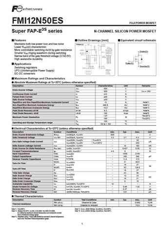
fmp12n50es.pdf
FMP12N50ES FUJI POWER MOSFET Super FAP-E3S series N-CHANNEL SILICON POWER MOSFET Features Outline Drawings [mm] Equivalent circuit schematic Maintains both low power loss and low noise TO-220AB Lower R (on) characteristic DS More controllable switching dv/dt by gate resistance Drain(D) Smaller V ringing waveform during switching GS Narrow band of the gate threshold voltage (3.7 0.5V
fml12n50es.pdf
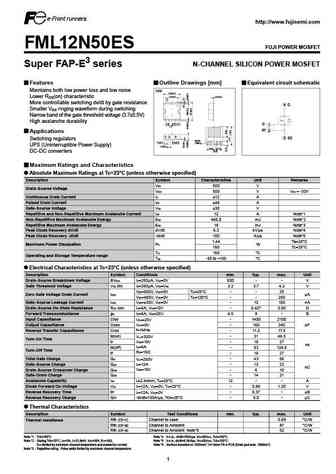
http //www.fujisemi.com FML12N50ES FUJI POWER MOSFET Super FAP-E3 series N-CHANNEL SILICON POWER MOSFET Features Outline Drawings [mm] Equivalent circuit schematic Maintains both low power loss and low noise TFP 9.0 0.2 7.0 0.2 0.4 0.1 Lower R (on) characteristic DS 4 More controllable switching dv/dt by gate resistance 4 D Smaller V ringing waveform during switching GS Narrow
fmv12n50es.pdf
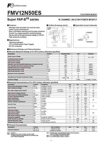
FMV12N50ES FUJI POWER MOSFET Super FAP-E3S series N-CHANNEL SILICON POWER MOSFET Features Outline Drawings [mm] Equivalent circuit schematic Maintains both low power loss and low noise TO-220F (SLS) Lower R (on) characteristic DS More controllable switching dv/dt by gate resistance Drain(D) Smaller V ringing waveform during switching GS Narrow band of the gate threshold voltage (3.
fmp12n50e.pdf

FMP12N50E FUJI POWER MOSFET Super FAP-E3 series N-CHANNEL SILICON POWER MOSFET Features Outline Drawings [mm] Equivalent circuit schematic Maintains both low power loss and low noise TO-220AB Lower R (on) characteristic DS More controllable switching dv/dt by gate resistance Drain(D) Smaller V ringing waveform during switching GS Narrow band of the gate threshold voltage (3.0 0.5V)
fmv12n50e.pdf
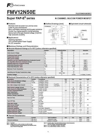
FMV12N50E FUJI POWER MOSFET Super FAP-E3 series N-CHANNEL SILICON POWER MOSFET Features Outline Drawings [mm] Equivalent circuit schematic Maintains both low power loss and low noise TO-220F(SLS) Lower R (on) characteristic DS More controllable switching dv/dt by gate resistance Drain(D) Smaller V ringing waveform during switching GS Narrow band of the gate threshold voltage (3.0 0.

mtp2n50e.pdf
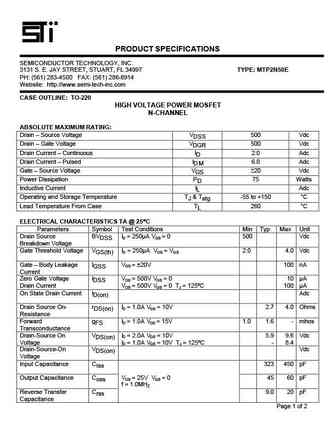
PRODUCT SPECIFICATIONS SEMICONDUCTOR TECHNOLOGY, INC. 3131 S. E. JAY STREET, STUART, FL 34997 TYPE MTP2N50E PH (561) 283-4500 FAX (561) 286-8914 Website http //www.semi-tech-inc.com CASE OUTLINE TO-220 HIGH VOLTAGE POWER MOSFET N-CHANNEL ABSOLUTE MAXIMUM RATING Drain Source Voltage VDSS 500 Vdc Drain Gate Voltage VDGR 500 Vdc Drain Current Continuous ID 2
2n5001smd.pdf

2N5001SMD Dimensions in mm (inches). Bipolar PNP Device in a Hermetically sealed 0.89 (0.035) min. Ceramic Surface Mount 3.70 (0.146) 3.70 (0.146) 3.60 (0.142) 3.41 (0.134) 3.41 (0.134) Max. Package for High Reliability Applications 1 3 Bipolar PNP Device. 2 VCEO = 80V IC = 2A 9.67 (0.381) All Semelab hermetically sealed products 9.38 (0.369) 0.50 (0.020) 0.26 (0
2n5052smd.pdf
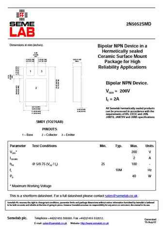
2N5052SMD Dimensions in mm (inches). Bipolar NPN Device in a Hermetically sealed 0.89 (0.035) min. Ceramic Surface Mount 3.70 (0.146) 3.70 (0.146) 3.60 (0.142) 3.41 (0.134) 3.41 (0.134) Max. Package for High Reliability Applications 1 3 Bipolar NPN Device. 2 VCEO = 200V IC = 2A 9.67 (0.381) All Semelab hermetically sealed products 9.38 (0.369) 0.50 (0.020) 0.26 (
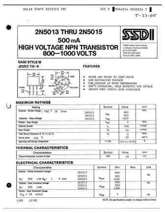
2n5015.pdf

2N5015 Dimensions in mm (inches). Bipolar NPN Device in a 8.51 (0.34) 9.40 (0.37) Hermetically sealed TO39 7.75 (0.305) 8.51 (0.335) Metal Package. 6.10 (0.240) 6.60 (0.260) Bipolar NPN Device. 0.89 max. (0.035) 12.70 (0.500) min. 0.41 (0.016) 0.53 (0.021) VCEO = 1000V dia. IC = 0.5A 5.08 (0.200) typ. 2.54 All Semelab hermetically sealed products 2 (0.100)
2n5013.pdf

2N5013 Dimensions in mm (inches). Bipolar NPN Device in a 8.51 (0.34) 9.40 (0.37) Hermetically sealed TO39 7.75 (0.305) 8.51 (0.335) Metal Package. 6.10 (0.240) 6.60 (0.260) Bipolar NPN Device. 0.89 max. (0.035) 12.70 (0.500) min. 0.41 (0.016) 0.53 (0.021) VCEO = 800V dia. IC = 0.5A 5.08 (0.200) typ. 2.54 All Semelab hermetically sealed products 2 (0.100) 1
2n5095.pdf
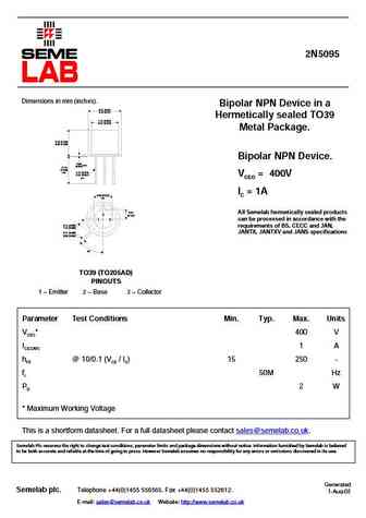
2N5095 Dimensions in mm (inches). Bipolar NPN Device in a 8.51 (0.34) 9.40 (0.37) Hermetically sealed TO39 7.75 (0.305) 8.51 (0.335) Metal Package. 6.10 (0.240) 6.60 (0.260) Bipolar NPN Device. 0.89 max. (0.035) 12.70 (0.500) min. 0.41 (0.016) 0.53 (0.021) VCEO = 400V dia. IC = 1A 5.08 (0.200) typ. 2.54 All Semelab hermetically sealed products 2 (0.100) 1 3
2n5099.pdf

2N5099 Dimensions in mm (inches). Bipolar NPN Device in a 8.51 (0.34) 9.40 (0.37) Hermetically sealed TO39 7.75 (0.305) 8.51 (0.335) Metal Package. 6.10 (0.240) 6.60 (0.260) Bipolar NPN Device. 0.89 max. (0.035) 12.70 (0.500) min. 0.41 (0.016) 0.53 (0.021) VCEO = 550V dia. IC = 1A 5.08 (0.200) typ. 2.54 All Semelab hermetically sealed products 2 (0.100) 1 3
2n5014.pdf
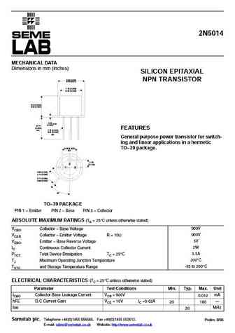
2N5014 MECHANICAL DATA Dimensions in mm (inches) SILICON EPITAXIAL NPN TRANSISTOR FEATURES General purpose power transistor for switch- ing and linear applications in a hermetic TO 39 package.
2n5012.pdf
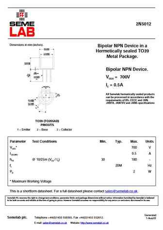
2N5012 Dimensions in mm (inches). Bipolar NPN Device in a 8.51 (0.34) 9.40 (0.37) Hermetically sealed TO39 7.75 (0.305) 8.51 (0.335) Metal Package. 6.10 (0.240) 6.60 (0.260) Bipolar NPN Device. 0.89 max. (0.035) 12.70 (0.500) min. 0.41 (0.016) 0.53 (0.021) VCEO = 700V dia. IC = 0.5A 5.08 (0.200) typ. 2.54 All Semelab hermetically sealed products 2 (0.100) 1
2n5011.pdf

2N5011 Dimensions in mm (inches). Bipolar NPN Device in a 8.51 (0.34) 9.40 (0.37) Hermetically sealed TO39 7.75 (0.305) 8.51 (0.335) Metal Package. 6.10 (0.240) 6.60 (0.260) Bipolar NPN Device. 0.89 max. (0.035) 12.70 (0.500) min. 0.41 (0.016) 0.53 (0.021) VCEO = 600V dia. IC = 0.5A 5.08 (0.200) typ. 2.54 All Semelab hermetically sealed products 2 (0.100) 1
2n5015x.pdf
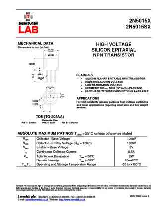
2N5015X 2N5015SX MECHANICAL DATA HIGH VOLTAGE Dimensions in mm (inches) 8.51 (0.34) 9.40 (0.37) SILICON EPITAXIAL 7.75 (0.305) 8.51 (0.335) NPN TRANSISTOR 6.10 (0.240) 6.60 (0.260) 0.89 max. (0.035) 38.00 (1.5) FEATURES min. 0.41 (0.016) 0.53 (0.021) SILICON PLANAR EPITAXIAL NPN TRANSISTOR dia. HIGH BREAKDOWN VOLTAGE LOW SATURATION VOLTAGE 5.08 (0.20
2n5038 2n5039.pdf
A Boca Semiconductor Corp. (BSC) http //www.bocasemi.com A http //www.bocasemi.com http //www.bocasemi.com
2n5088 89.pdf
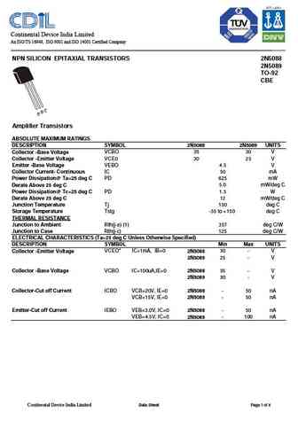
Continental Device India Limited An ISO/TS 16949, ISO 9001 and ISO 14001 Certified Company NPN SILICON EPITAXIAL TRANSISTORS 2N5088 2N5089 TO-92 CBE C B E Amplifier Transistors ABSOLUTE MAXIMUM RATINGS DESCRIPTION SYMBOL 2N5088 2N5089 UNITS Collector -Base Voltage VCBO 35 30 V Collector -Emitter Voltage VCE0 30 25 V Emitter -Base Voltage VEBO 4.5 V Collector Current- Continuous I
2n5020 2n5021.pdf
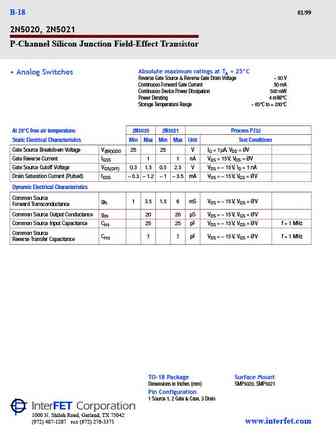
Databook.fxp 1/13/99 2 09 PM Page B-18 B-18 01/99 2N5020, 2N5021 P-Channel Silicon Junction Field-Effect Transistor Absolute maximum ratings at TA = 25 C Analog Switches Reverse Gate Source & Reverse Gate Drain Voltage 50 V Continuous Forward Gate Current 50 mA Continuous Device Power Dissipation 500 mW Power Derating 4 mW/ C Storage Temperature Range 65 C to + 200 C A
2n5038 2n5039.pdf
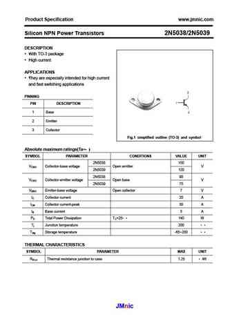
Product Specification www.jmnic.com Silicon NPN Power Transistors 2N5038/2N5039 DESCRIPTION With TO-3 package High current APPLICATIONS They are especially intended for high current and fast switching applications PINNING PIN DESCRIPTION 1 Base 2 Emitter 3 Collector Fig.1 simplified outline (TO-3) and symbol Absolute maximum ratings(Ta= ) SYMBOL PARAMETER COND
2n5050 2n5051 2n5052.pdf
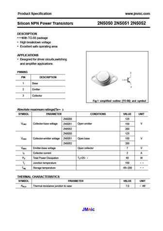
Product Specification www.jmnic.com Silicon NPN Power Transistors 2N5050 2N5051 2N5052 DESCRIPTION With TO-66 package High breakdown voltage Excellent safe operating area APPLICATIONS Designed for driver circuits,switching and amplifier applications PINNING PIN DESCRIPTION 1 Base 2 Emitter 3 Collector Fig.1 simplified outline (TO-66) and symbol Absolute ma
2n5067 2n5068 2n5069.pdf
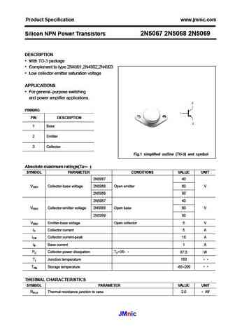
Product Specification www.jmnic.com Silicon NPN Power Transistors 2N5067 2N5068 2N5069 DESCRIPTION With TO-3 package Complement to type 2N4901,2N4902,2N4903 Low collector-emitter saturation voltage APPLICATIONS For general purpose switching and power amplifier applications. PINNING PIN DESCRIPTION 1 Base 2 Emitter 3 Collector Fig.1 simplified outline (TO-3) an
2n5018 2n5019.pdf
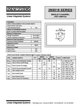
2N5018 SERIES SINGLE P-CHANNEL Linear Integrated Systems JFET SWITCH FEATURES DIRECT REPLACEMENT FOR SILICONIX 2N5018 ZERO OFFSET VOLTAGE LOW ON RESISTANCE 75 TO-18 ABSOLUTE MAXIMUM RATINGS1 BOTTOM VIEW @ 25 C (unless otherwise stated) Maximum Temperatures G 2 3 D Storage Temperature -55 to 200 C Junction Operating Temperature -55 to 200 C 1 S Maximum Powe
2n5011s.pdf

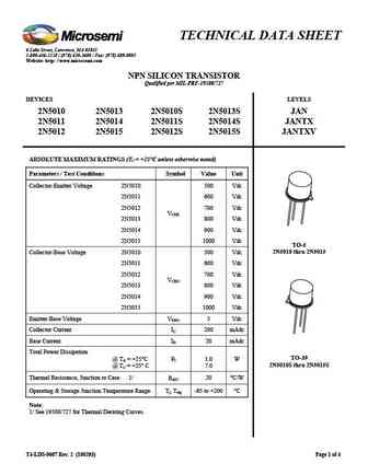
TECHNICAL DATA SHEET 6 Lake Street, Lawrence, MA 01841 1-800-446-1158 / (978) 620-2600 / Fax (978) 689-0803 Website http //www.microsemi.com NPN SILICON TRANSISTOR Qualified per MIL-PRF-19500/727 DEVICES LEVELS 2N5010 2N5013 2N5010S 2N5013S JAN 2N5011 2N5014 2N5011S 2N5014S JANTX 2N5012 2N5015 2N5012S 2N5015S JANTXV ABSOLUTE MAXIMUM RATINGS (TC = +25 C unless otherwise note
2n5014s.pdf

TECHNICAL DATA SHEET 6 Lake Street, Lawrence, MA 01841 1-800-446-1158 / (978) 620-2600 / Fax (978) 689-0803 Website http //www.microsemi.com NPN SILICON TRANSISTOR Qualified per MIL-PRF-19500/727 DEVICES LEVELS 2N5010 2N5013 2N5010S 2N5013S JAN 2N5011 2N5014 2N5011S 2N5014S JANTX 2N5012 2N5015 2N5012S 2N5015S JANTXV ABSOLUTE MAXIMUM RATINGS (TC = +25 C unless otherwise note
2n5015sx.pdf
TECHNICAL DATA SHEET 6 Lake Street, Lawrence, MA 01841 1-800-446-1158 / (978) 620-2600 / Fax (978) 689-0803 Website http //www.microsemi.com NPN SILICON TRANSISTOR Qualified per MIL-PRF-19500/727 DEVICES LEVELS 2N5010 2N5013 2N5010S 2N5013S JAN 2N5011 2N5014 2N5011S 2N5014S JANTX 2N5012 2N5015 2N5012S 2N5015S JANTXV ABSOLUTE MAXIMUM RATINGS (TC = +25 C unless otherwise note
msaer12n50a msafr12n50a.pdf
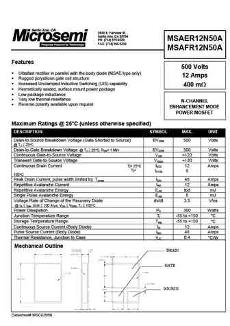
2830 S. Fairview St. Santa Ana, CA 92704 PH (714) 979-8220 MSAER12N50A FAX (714) 966-5256 MSAFR12N50A Features 500 Volts Ultrafast rectifier in parallel with the body diode (MSAE type only) 12 Amps Rugged polysilicon gate cell structure Increased Unclamped Inductive Switching (UIS) capability 400 m Hermetically sealed, surface mount power package Low p
12n50a.pdf
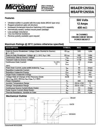
2830 S. Fairview St. Santa Ana, CA 92704 PH (714) 979-8220 MSAER12N50A FAX (714) 966-5256 MSAFR12N50A Features 500 Volts Ultrafast rectifier in parallel with the body diode (MSAE type only) 12 Amps Rugged polysilicon gate cell structure Increased Unclamped Inductive Switching (UIS) capability 400 m Hermetically sealed, surface mount power package Low p
2n5013s.pdf

TECHNICAL DATA SHEET 6 Lake Street, Lawrence, MA 01841 1-800-446-1158 / (978) 620-2600 / Fax (978) 689-0803 Website http //www.microsemi.com NPN SILICON TRANSISTOR Qualified per MIL-PRF-19500/727 DEVICES LEVELS 2N5010 2N5013 2N5010S 2N5013S JAN 2N5011 2N5014 2N5011S 2N5014S JANTX 2N5012 2N5015 2N5012S 2N5015S JANTXV ABSOLUTE MAXIMUM RATINGS (TC = +25 C unless otherwise note
2n5012s.pdf

TECHNICAL DATA SHEET 6 Lake Street, Lawrence, MA 01841 1-800-446-1158 / (978) 620-2600 / Fax (978) 689-0803 Website http //www.microsemi.com NPN SILICON TRANSISTOR Qualified per MIL-PRF-19500/727 DEVICES LEVELS 2N5010 2N5013 2N5010S 2N5013S JAN 2N5011 2N5014 2N5011S 2N5014S JANTX 2N5012 2N5015 2N5012S 2N5015S JANTXV ABSOLUTE MAXIMUM RATINGS (TC = +25 C unless otherwise note
2n5031.pdf
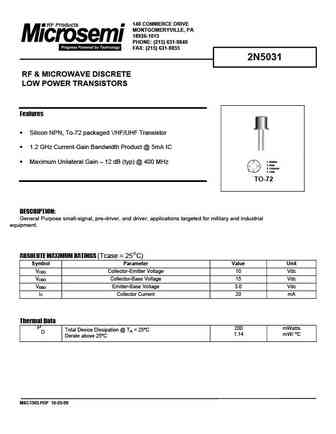
140 COMMERCE DRIVE MONTGOMERYVILLE, PA 18936-1013 PHONE (215) 631-9840 FAX (215) 631-9855 2N5031 RF & MICROWAVE DISCRETE LOW POWER TRANSISTORS Features Silicon NPN, To-72 packaged VHF/UHF Transistor 1.2 GHz Current-Gain Bandwidth Product @ 5mA IC 2 1. Emitter Maximum Unilateral Gain 12 dB (typ) @ 400 MHz 2. Base 1 3 3. Collector 4 4. Case TO-72 DESCRIPTION
2n5010s.pdf

TECHNICAL DATA SHEET 6 Lake Street, Lawrence, MA 01841 1-800-446-1158 / (978) 620-2600 / Fax (978) 689-0803 Website http //www.microsemi.com NPN SILICON TRANSISTOR Qualified per MIL-PRF-19500/727 DEVICES LEVELS 2N5010 2N5013 2N5010S 2N5013S JAN 2N5011 2N5014 2N5011S 2N5014S JANTX 2N5012 2N5015 2N5012S 2N5015S JANTXV ABSOLUTE MAXIMUM RATINGS (TC = +25 C unless otherwise note
2n5005.pdf
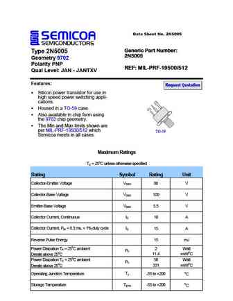
Data Sheet No. 2N5005 Generic Part Number Type 2N5005 2N5005 Geometry 9702 Polarity PNP REF MIL-PRF-19500/512 Qual Level JAN - JANTXV Features Silicon power transistor for use in high speed power switching appli- cations. Housed in a TO-59 case. Also available in chip form using the 9702 chip geometry. The Min and Max limits shown are per MIL-PRF-19500/512 wh
2n5003.pdf
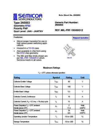
Data Sheet No. 2N5003 Generic Part Number Type 2N5003 2N5003 Geometry 9702 Polarity PNP REF MIL-PRF-19500/512 Qual Level JAN - JANTXV Features Silicon power transistor for use in high speed power switching appli- cations. Housed in a TO-59 case. Also available in chip form using the 9702 chip geometry. The Min and Max limits shown are TO-59 per MIL-PRF-19500
2n5002.pdf
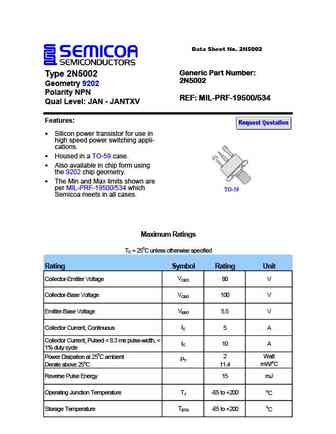
Data Sheet No. 2N5002 Generic Part Number Type 2N5002 2N5002 Geometry 9202 Polarity NPN REF MIL-PRF-19500/534 Qual Level JAN - JANTXV Features Silicon power transistor for use in high speed power switching appli- cations. Housed in a TO-59 case. Also available in chip form using the 9202 chip geometry. The Min and Max limits shown are per MIL-PRF-19500/534 wh
2n5004.pdf
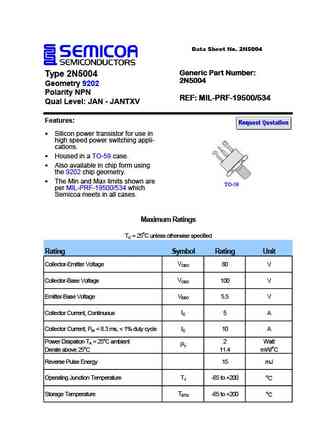
Data Sheet No. 2N5004 Generic Part Number Type 2N5004 2N5004 Geometry 9202 Polarity NPN REF MIL-PRF-19500/534 Qual Level JAN - JANTXV Features Silicon power transistor for use in high speed power switching appli- cations. Housed in a TO-59 case. Also available in chip form using the 9202 chip geometry. The Min and Max limits shown are TO-59 per MIL-PRF-19500
h2n5087.pdf
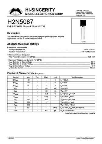
Spec. No. HE6210 HI-SINCERITY Issued Date 1998.02.01 Revised Date 2005.01.20 MICROELECTRONICS CORP. Page No. 1/5 H2N5087 PNP EPITAXIAL PLANAR TRANSISTOR Description This device was designed for low noise,high gain,general purpose amplifier applications for 1uA to 25mA collector current. TO-92 Absolute Maximum Ratings Maximum Temperatures Storage Temperature ...........
aok22n50l.pdf
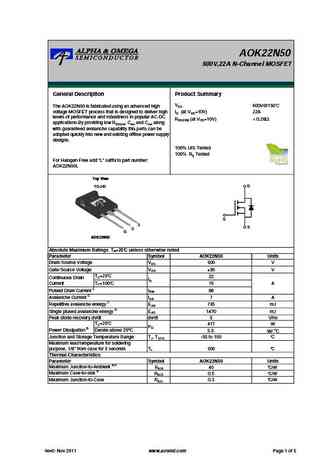
AOK22N50 500V,22A N-Channel MOSFET General Description Product Summary VDS 600V@150 The AOK22N50 is fabricated using an advanced high voltage MOSFET process that is designed to deliver high ID (at VGS=10V) 22A levels of performance and robustness in popular AC-DC RDS(ON) (at VGS=10V)
aob12n50l.pdf
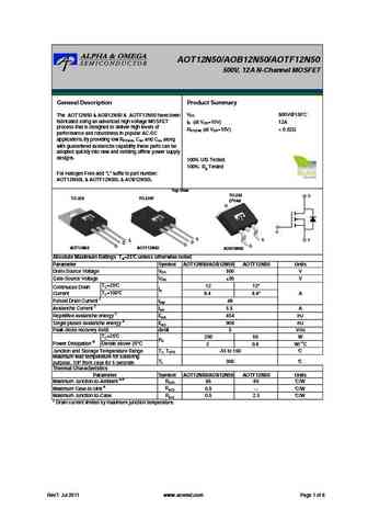
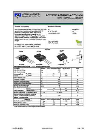
AOT12N50/AOB12N50/AOTF12N50 500V, 12A N-Channel MOSFET General Description Product Summary VDS 600V@150 The AOT12N50 & AOB12N50 & AOTF12N50 have been fabricated using an advanced high voltage MOSFET ID (at VGS=10V) 12A process that is designed to deliver high levels of RDS(ON) (at VGS=10V)
aotf12n50.pdf

AOT12N50/AOB12N50/AOTF12N50 500V, 12A N-Channel MOSFET General Description Product Summary VDS 600V@150 The AOT12N50 & AOB12N50 & AOTF12N50 have been fabricated using an advanced high voltage MOSFET ID (at VGS=10V) 12A process that is designed to deliver high levels of RDS(ON) (at VGS=10V)
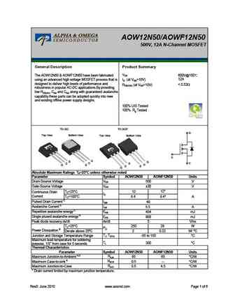
aow12n50.pdf
AOW12N50/AOWF12N50 500V, 12A N-Channel MOSFET General Description Product Summary VDS The AOW12N50 & AOWF12N50 have been fabricated 600V@150 12A using an advanced high voltage MOSFET process that is ID (at VGS=10V) designed to deliver high levels of performance and
aotf22n50.pdf
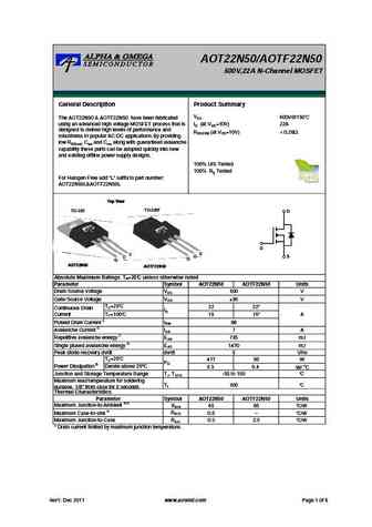
AOT22N50/AOTF22N50 500V,22A N-Channel MOSFET General Description Product Summary VDS 600V@150 The AOT22N50 & AOTF22N50 have been fabricated using an advanced high voltage MOSFET process that is ID (at VGS=10V) 22A designed to deliver high levels of performance and RDS(ON) (at VGS=10V)
aowf12n50.pdf

AOW12N50/AOWF12N50 500V, 12A N-Channel MOSFET General Description Product Summary VDS The AOW12N50 & AOWF12N50 have been fabricated 600V@150 12A using an advanced high voltage MOSFET process that is ID (at VGS=10V) designed to deliver high levels of performance and
aot12n50.pdf

AOT12N50/AOB12N50/AOTF12N50 500V, 12A N-Channel MOSFET General Description Product Summary VDS 600V@150 The AOT12N50 & AOB12N50 & AOTF12N50 have been fabricated using an advanced high voltage MOSFET ID (at VGS=10V) 12A process that is designed to deliver high levels of RDS(ON) (at VGS=10V)
aot12n50 aob12n50 aotf12n50.pdf

AOT12N50/AOB12N50/AOTF12N50 500V, 12A N-Channel MOSFET General Description Product Summary VDS 600V@150 The AOT12N50 & AOB12N50 & AOTF12N50 have been fabricated using an advanced high voltage MOSFET ID (at VGS=10V) 12A process that is designed to deliver high levels of RDS(ON) (at VGS=10V)
aok22n50.pdf
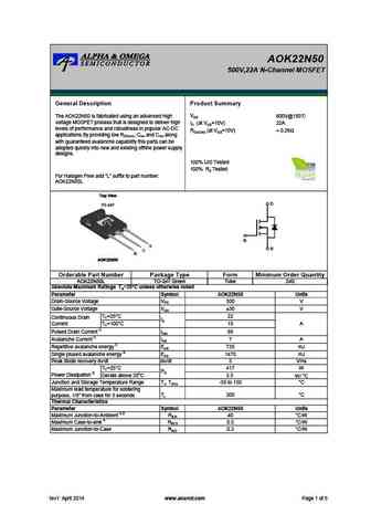
AOK22N50 500V,22A N-Channel MOSFET General Description Product Summary VDS 600V@150 The AOK22N50 is fabricated using an advanced high voltage MOSFET process that is designed to deliver high ID (at VGS=10V) 22A levels of performance and robustness in popular AC-DC RDS(ON) (at VGS=10V)
aow12n50 aowf12n50.pdf
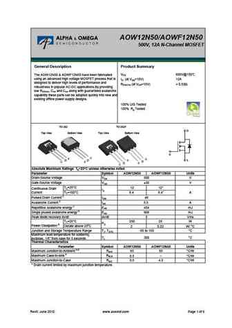
AOW12N50/AOWF12N50 500V, 12A N-Channel MOSFET General Description Product Summary VDS 600V@150 The AOW12N50 & AOWF12N50 have been fabricated using an advanced high voltage MOSFET process that is ID (at VGS=10V) 12A designed to deliver high levels of performance and RDS(ON) (at VGS=10V)
aot22n50l.pdf

AOT22N50/AOTF22N50 500V,22A N-Channel MOSFET General Description Product Summary VDS 600V@150 The AOT22N50 & AOTF22N50 have been fabricated using an advanced high voltage MOSFET process that is ID (at VGS=10V) 22A designed to deliver high levels of performance and RDS(ON) (at VGS=10V)
aot22n50.pdf

AOT22N50/AOTF22N50 500V,22A N-Channel MOSFET General Description Product Summary VDS 600V@150 The AOT22N50 & AOTF22N50 have been fabricated using an advanced high voltage MOSFET process that is ID (at VGS=10V) 22A designed to deliver high levels of performance and RDS(ON) (at VGS=10V)
aob12n50.pdf
AOT12N50/AOB12N50/AOTF12N50 500V, 12A N-Channel MOSFET General Description Product Summary VDS 600V@150 The AOT12N50 & AOB12N50 & AOTF12N50 have been fabricated using an advanced high voltage MOSFET ID (at VGS=10V) 12A process that is designed to deliver high levels of RDS(ON) (at VGS=10V)
aot22n50 aotf22n50.pdf
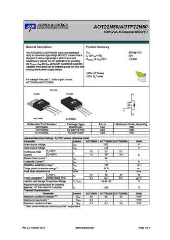
AOT22N50/AOTF22N50 500V,22A N-Channel MOSFET General Description Product Summary VDS 600V@150 The AOT22N50 & AOTF22N50 have been fabricated using an advanced high voltage MOSFET process that is ID (at VGS=10V) 22A designed to deliver high levels of performance and RDS(ON) (at VGS=10V)
jcs22n50fc.pdf
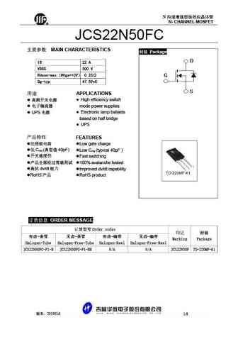
N N- CHANNEL MOSFET R JCS22N50FC MAIN CHARACTERISTICS Package ID 22 A VDSS 500 V Rdson-max @Vgs=10V 0.25 Qg-typ 47.59nC APPLICATIONS High efficiency switch mode power supplies Electronic lamp ballasts UPS based on half bridge U
jcs22n50abc jcs22n50wc.pdf
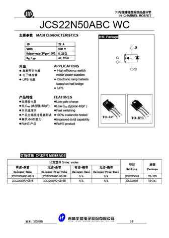
N N- CHANNEL MOSFET R JCS22N50ABC WC MAIN CHARACTERISTICS Package ID 22 A VDSS 500 V Rdson-max @Vgs=10V 0.25 Qg-typ 47.59nC APPLICATIONS High efficiency switch mode power supplies Electronic lamp ballasts UPS based on half bridge
kqb2n50.pdf
SMD Type SMD Type SMD Type IC SMD Type IC SMD Type IC SMD Type IC SMD Type IC SMD Type Transistors SMD Type Transistors SMD Type Transistors SMD Type Transistors SMD Type Transistors SMD Type SMD Type SMD Type SMD Type SMD Type SMD Type SMD Type SMD Type SMD Type SMD Type Product specification KQB2N50 TO-263 Unit mm Features 4.57+0.2 -0.2 +0.1 1.27-0.1 2.1A, 500
mdp12n50th.pdf
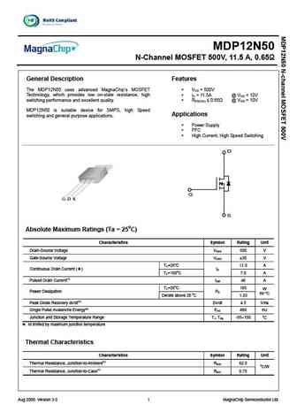
MDP12N50 N-Channel MOSFET 500V, 11.5 A, 0.65 General Description Features The MDP12N50 uses advanced MagnaChip s MOSFET V = 500V DS Technology, which provides low on-state resistance, high I = 11.5A @ V = 10V D GS switching performance and excellent quality. R 0.65 @ V = 10V DS(ON) GS MDP12N50 is suitable device for SMPS, high Speed Applications switching and ge
mdf12n50bth mdp12n50bth.pdf
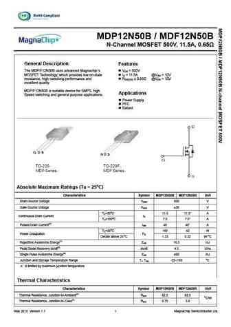
MDP12N50B / MDF12N50B N-Channel MOSFET 500V, 11.5A, 0.65 General Description Features The MDP/F12N50B uses advanced Magnachip s VDS = 500V MOSFET Technology, which provides low on-state ID = 11.5A @VGS = 10V resistance, high switching performance and RDS(ON) 0.65 @VGS = 10V excellent quality. MDP/F12N50B is suitable device for SMPS, high Applications Speed switc
mdf12n50fth mdp12n50fth.pdf
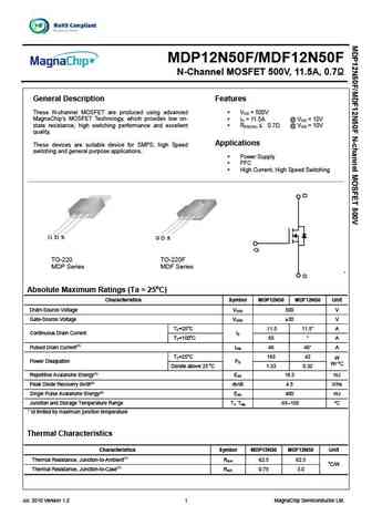
MDP12N50F/MDF12N50F N-Channel MOSFET 500V, 11.5A, 0.7 General Description Features These N-channel MOSFET are produced using advanced V = 500V DS MagnaChip s MOSFET Technology, which provides low on- I = 11.5A @ V = 10V D GS state resistance, high switching performance and excellent R 0.7 @ V = 10V DS(ON) GS quality. Applications These devices are suitable devic
bl2n50-p bl2n50-a bl2n50-u bl2n50-d.pdf
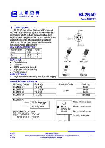
BL2N50 Power MOSFET 1 Description Step-Down Converter BL2N50, the silicon N-channel Enhanced , MOSFETs, is obtained by advanced MOSFET technology which reduce the conduction loss, improve switching performance and enhance the avalanche energy. The transistor is suitable device for SMPS, high speed switching and general purpose applications. KEY CHARACTERISTICS Para
qm12n50f.pdf
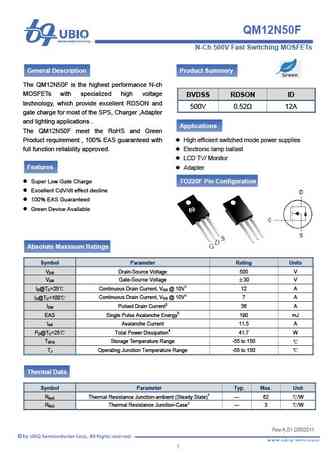
QM12N50F 1 2011-07-01 - 1 - N-Ch 500V Fast Switching MOSFETs General Description Product Summery The QM12N50F is the highest performance N-ch MOSFETs with specialized high voltage BVDSS RDSON ID technology, which provide excellent RDSON and 500V 0.52 12A gate charge for most of the SPS, Charger ,Adapter and lighting applications . Applications The QM12N50F m
wm02n50m.pdf
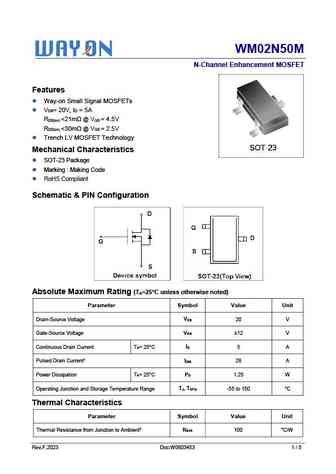
WM02N50M N-Channel Enhancement MOSFET Features Way-on Small Signal MOSFETs V = 20V, I = 5A DS D R
wmn22n50c4 wmm22n50c4 wmj22n50c4 wmo22n50c4 wmk22n50c4 wml22n50c4.pdf
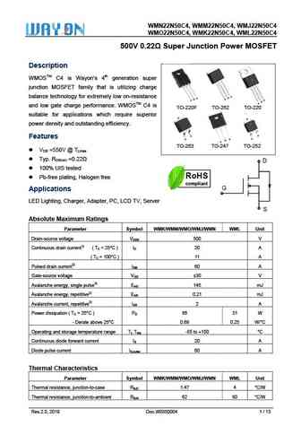
WMN22N50C4, WMM22N MJ22N50C N50C4, WM C4 WMO22N50C4, WMK22N ML22N50C N50C4, WM C4 500V n Power MOSFET V 0.22 Super Junction Descrip ption WMOSTM C4 is Wa 4th generation super ayon s n junction MOSFET fa that is utilizing charge M amily S balance te or extremely esistance echnology fo y low on-re S D D G G G S D G and low ga charge performanc WMOSTM C4
cs2n50a4.pdf
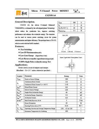
Silicon N-Channel Power MOSFET R CS2N50 A4 General Description VDSS 500 V CS2N50 A4, the silicon N-channel Enhanced ID 2 A PD (TC=25 ) 30 W VDMOSFETs, is obtained by the self-aligned planar Technology RDS(ON)Typ 5.5 which reduce the conduction loss, improve switching performance and enhance the avalanche energy. The transistor can be used in various power s
cs2n50df cs2n50dp cs2n50dd cs2n50du.pdf
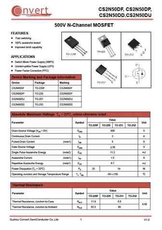
CS2N50DF, CS2N50DP, nvert Suzhou Convert Semiconductor Co ., Ltd. CS2N50DD,CS2N50DU 500V N-Channel MOSFET FEATURES Fast switching 100% avalanche tested Improved dv/dt capability APPLICATIONS Switch Mode Power Supply (SMPS) Uninterruptible Power Supply (UPS) Power Factor Correction (PFC) Device Marking and Package Information Device Package Marking CS2N50D
2n4265 2n4400 2n4401 2n4402 2n4403 2n4409 2n4410 2n4424 2n4425 2n4951 2n4952 2n4953 2n4954 2n5087 2n5088 2n5089.pdf
se12n50fra.pdf
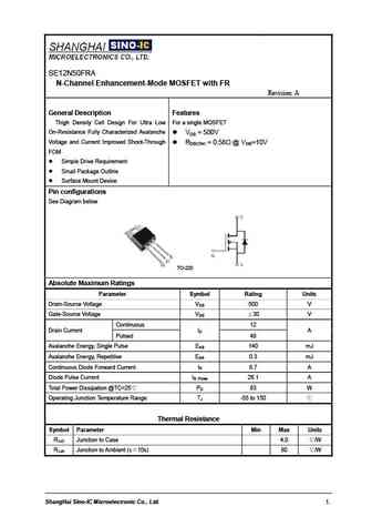
SE12N50FRA N-Channel Enhancement-Mode MOSFET with FR Revision A General Description Features Thigh Density Cell Design For Ultra Low For a single MOSFET On-Resistance Fully Characterized Avalanche VDS = 500V Voltage and Current Improved Shoot-Through RDS(ON) = 0.58 @ VGS=10V FOM Simple Drive Requirement Small Package Outline Surface Mount Device
fdb12n50f.pdf
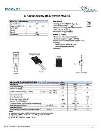
FDB12N50F www.VBsemi.tw Power MOSFET N-Channel 650V (D-S) FEATURES PRODUCT SUMMARY VDS (V) at TJ max. 670 Low figure-of-merit (FOM) Ron x Qg Low input capacitance (Ciss) RDS(on) max. at 25 C ( ) VGS = 10 V 0.67 Reduced switching and conduction losses Qg max. (nC) 41 Ultra low gate charge (Qg) Qgs (nC) 5 Avalanche energy rated (UIS) Qgd (nC) 22 Configurati
tma12n50h.pdf
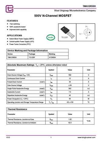
TMA12N50H Wuxi Unigroup Microelectronics Company 500V N-Channel MOSFET FEATURES Fast switching 100% avalanche tested Improved dv/dt capability APPLICATIONS Switch Mode Power Supply (SMPS) Uninterruptible Power Supply (UPS) Power Factor Correction (PFC) Device Marking and Package Information Device Package Marking TMA12N50H TO-220F A12N50H Abs
2n5038.pdf
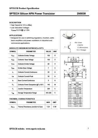
SPTECH Product Specification SPTECH Silicon NPN Power Transistor 2N5038 DESCRIPTION High Speed-t = 0.5 s (Max) f Low Saturation Voltage- V 2.5V@ I = 20A CE(sat) C APPLICATIONS Designed for use in switching regulators, inverters, wide- band amplifiers and power oscillators in industrial and commercial applications. ABSOLUTE MAXIMUM RATINGS(T =25 ) a SYMBOL PARAMETER VAL
mtp2n50.pdf
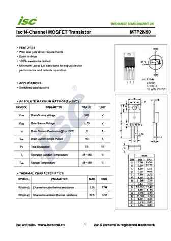
INCHANGE Semiconductor Isc N-Channel MOSFET Transistor MTP2N50 FEATURES With low gate drive requirements Easy to drive 100% avalanche tested Minimum Lot-to-Lot variations for robust device performance and reliable operation APPLICATIONS Switching applications ABSOLUTE MAXIMUM RATINGS(T =25 ) a SYMBOL PARAMETER VALUE UNIT V Drain-Source Voltage 500 V DSS V Gate-S
aok22n50l.pdf
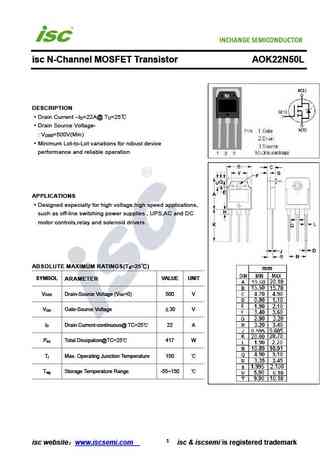
isc N-Channel MOSFET Transistor AOK22N50L DESCRIPTION Drain Current I =22A@ T =25 D C Drain Source Voltage- V =500V(Min) DSS Minimum Lot-to-Lot variations for robust device performance and reliable operation APPLICATIONS Designed especially for high voltage,high speed applications, such as off-line switching power supplies , UPS,AC and DC motor controls,relay and sol
irfp22n50a.pdf
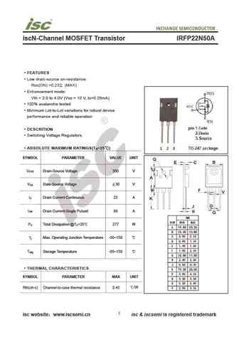
iscN-Channel MOSFET Transistor IRFP22N50A FEATURES Low drain-source on-resistance RDS(ON) =0.23 (MAX) Enhancement mode Vth = 2.0 to 4.0V (VDS = 10 V, ID=0.25mA) 100% avalanche tested Minimum Lot-to-Lot variations for robust device performance and reliable operation DESCRITION Switching Voltage Regulators ABSOLUTE MAXIMUM RATINGS(T =25 ) a SYMBOL PARAMETER VAL
mdp12n50bth.pdf
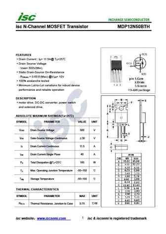
isc N-Channel MOSFET Transistor MDP12N50BTH FEATURES Drain Current I = 11.5A@ T =25 D C Drain Source Voltage V = 500V(Min) DSS Static Drain-Source On-Resistance R = 0.65 (Max) @V = 10V DS(on) GS 100% avalanche tested Minimum Lot-to-Lot variations for robust device performance and reliable operation DESCRIPTION motor drive, DC-DC converter, power switch and s
aotf12n50.pdf
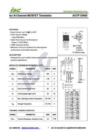
isc N-Channel MOSFET Transistor AOTF12N50 FEATURES Drain Current I =12A@ T =25 D C Drain Source Voltage- V =500V(Min) DSS Static Drain-Source On-Resistance R = 0.52 (Max) DS(on) 100% avalanche tested Minimum Lot-to-Lot variations for robust device performance and reliable operation DESCRIPTION Designed for use in switch mode power supplies and general purpo
spw52n50c3.pdf
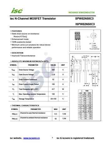
isc N-Channel MOSFET Transistor SPW52N50C3 ISPW52N50C3 FEATURES Static drain-source on-resistance RDS(on) 70m Enhancement mode 100% avalanche tested Minimum Lot-to-Lot variations for robust device performance and reliable operation DESCRITION Improved Transconductance ABSOLUTE MAXIMUM RATINGS(T =25 ) a SYMBOL PARAMETER VALUE UNIT V Drain-Source Voltage 500
spw32n50c3.pdf

isc N-Channel MOSFET Transistor SPW32N50C3 ISPW32N50C3 FEATURES Static drain-source on-resistance RDS(on) 110m Enhancement mode 100% avalanche tested Minimum Lot-to-Lot variations for robust device performance and reliable operation DESCRITION Improved Transconductance ABSOLUTE MAXIMUM RATINGS(T =25 ) a SYMBOL PARAMETER VALUE UNIT V Drain-Source Voltage 50
aow12n50.pdf
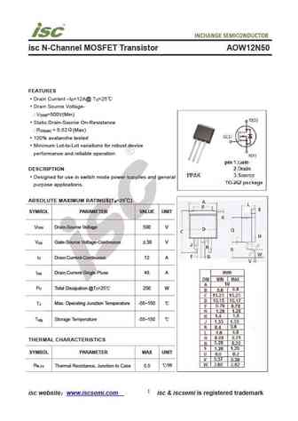
isc N-Channel MOSFET Transistor AOW12N50 FEATURES Drain Current I =12A@ T =25 D C Drain Source Voltage- V =500V(Min) DSS Static Drain-Source On-Resistance R = 0.52 (Max) DS(on) 100% avalanche tested Minimum Lot-to-Lot variations for robust device performance and reliable operation DESCRIPTION Designed for use in switch mode power supplies and general purpos
2n5038 2n5039.pdf
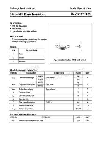
Inchange Semiconductor Product Specification Silicon NPN Power Transistors 2N5038 2N5039 DESCRIPTION With TO-3 package High speed Low collector saturation voltage APPLICATIONS They are especially intended for high current and fast switching applications PINNING PIN DESCRIPTION 1 Base 2 Emitter Fig.1 simplified outline (TO-3) and symbol 3 Collector Absolute max
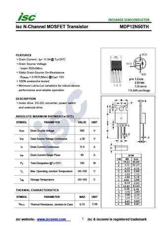
mdp12n50th.pdf
isc N-Channel MOSFET Transistor MDP12N50TH FEATURES Drain Current I = 11.5A@ T =25 D C Drain Source Voltage V = 500V(Min) DSS Static Drain-Source On-Resistance R = 0.65 (Max) @V = 10V DS(on) GS 100% avalanche tested Minimum Lot-to-Lot variations for robust device performance and reliable operation DESCRIPTION motor drive, DC-DC converter, power switch and so
aotf22n50.pdf
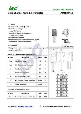
isc N-Channel MOSFET Transistor AOTF22N50 FEATURES Drain Current I = 22A@ T =25 D C Drain Source Voltage- V = 500V(Min) DSS Static Drain-Source On-Resistance R = 0.26 (Max) DS(on) 100% avalanche tested Minimum Lot-to-Lot variations for robust device performance and reliable operation DESCRIPTION Designed for use in switch mode power supplies and general pur
2n5050 2n5051 2n5052.pdf
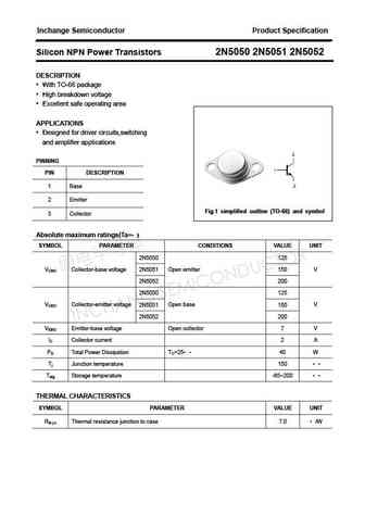
Inchange Semiconductor Product Specification Silicon NPN Power Transistors 2N5050 2N5051 2N5052 DESCRIPTION With TO-66 package High breakdown voltage Excellent safe operating area APPLICATIONS Designed for driver circuits,switching and amplifier applications PINNING PIN DESCRIPTION 1 Base 2 Emitter Fig.1 simplified outline (TO-66) and symbol 3 Collector Absolut
aot12n50.pdf

isc N-Channel MOSFET Transistor AOT12N50 FEATURES Drain Current I =12A@ T =25 D C Drain Source Voltage- V =500V(Min) DSS Static Drain-Source On-Resistance R = 0.52 (Max) DS(on) 100% avalanche tested Minimum Lot-to-Lot variations for robust device performance and reliable operation DESCRIPTION Designed for use in switch mode power supplies and general purpos
fmv12n50e.pdf
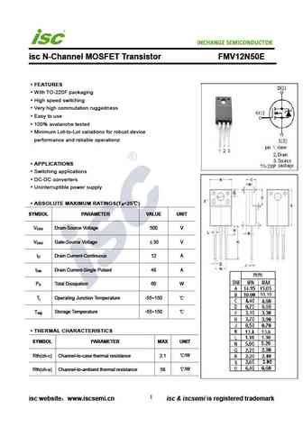
INCHANGE Semiconductor isc N-Channel MOSFET Transistor FMV12N50E FEATURES With TO-220F packaging High speed switching Very high commutation ruggedness Easy to use 100% avalanche tested Minimum Lot-to-Lot variations for robust device performance and reliable operationz APPLICATIONS Switching applications DC-DC converters Uninterruptible power supply ABSOLUTE
sihd12n50e.pdf
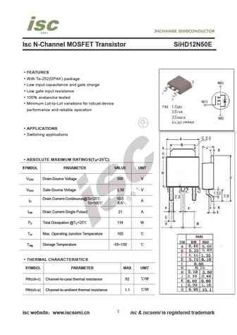
Isc N-Channel MOSFET Transistor SiHD12N50E FEATURES With To-252(DPAK) package Low input capacitance and gate charge Low gate input resistance 100% avalanche tested Minimum Lot-to-Lot variations for robust device performance and reliable operation APPLICATIONS Switching applications ABSOLUTE MAXIMUM RATINGS(T =25 ) a SYMBOL PARAMETER VALUE UNIT V Drain-Source Vol
2n5067 2n5068 2n5069.pdf
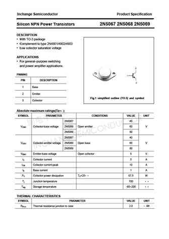
Inchange Semiconductor Product Specification Silicon NPN Power Transistors 2N5067 2N5068 2N5069 DESCRIPTION With TO-3 package Complement to type 2N4901/4902/4903 Low collector saturation voltage APPLICATIONS For general purpose switching and power amplifier applications. PINNING PIN DESCRIPTION 1 Base 2 Emitter Fig.1 simplified outline (TO-3) and symbol 3 Col
fdpf12n50nz.pdf
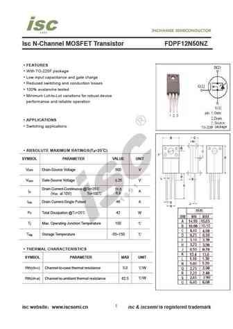
Isc N-Channel MOSFET Transistor FDPF12N50NZ FEATURES With TO-220F package Low input capacitance and gate charge Reduced switching and conduction losses 100% avalanche tested Minimum Lot-to-Lot variations for robust device performance and reliable operation APPLICATIONS Switching applications ABSOLUTE MAXIMUM RATINGS(T =25 ) a SYMBOL PARAMETER VALUE UNIT V Drain-
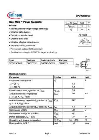
spd02n50c3.pdf
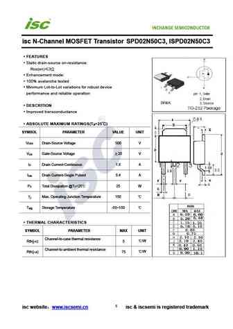
isc N-Channel MOSFET Transistor SPD02N50C3, ISPD02N50C3 FEATURES Static drain-source on-resistance RDS(on) 3 Enhancement mode 100% avalanche tested Minimum Lot-to-Lot variations for robust device performance and reliable operation DESCRITION Improved transconductance ABSOLUTE MAXIMUM RATINGS(T =25 ) a SYMBOL PARAMETER VALUE UNIT V Drain-Source Voltage 500 V
12n50.pdf
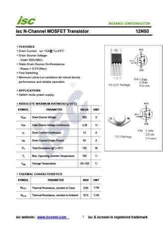
isc N-Channel MOSFET Transistor 12N50 FEATURES Drain Current I = 12A@ T =25 D C Drain Source Voltage- V = 500V(Min) DSS Static Drain-Source On-Resistance R = 0.5 (Max) DS(on) Fast Switching Minimum Lot-to-Lot variations for robust device performance and reliable operation APPLICATIONS Switch mode power supply. ABSOLUTE MAXIMUM RATINGS(T =25 ) a SYMBO
aok22n50.pdf
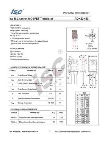
INCHANGE Semiconductor isc N-Channel MOSFET Transistor AOK22N50 FEATURES With TO-247 packaging High speed switching Very high commutation ruggedness Easy to use 100% avalanche tested Minimum Lot-to-Lot variations for robust device performance and reliable operation APPLICATIONS PFC stages LCD & PDP TV Power supply Switching applications ABSOLUTE MAXIMUM
spp12n50c3.pdf
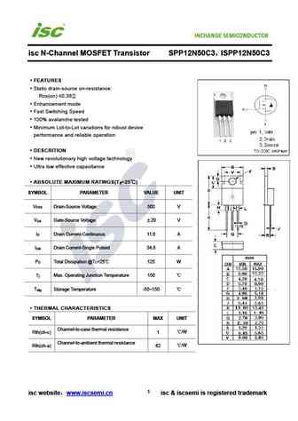
isc N-Channel MOSFET Transistor SPP12N50C3 ISPP12N50C3 FEATURES Static drain-source on-resistance RDS(on) 0.38 Enhancement mode Fast Switching Speed 100% avalanche tested Minimum Lot-to-Lot variations for robust device performance and reliable operation DESCRITION New revolutionary high voltage technology Ultra low effective capacitance ABSOLUTE MAXIMUM
fdp12n50nz.pdf
Isc N-Channel MOSFET Transistor FDP12N50NZ FEATURES With TO-220F package Low input capacitance and gate charge Reduced switching and conduction losses 100% avalanche tested Minimum Lot-to-Lot variations for robust device performance and reliable operation APPLICATIONS Switching applications ABSOLUTE MAXIMUM RATINGS(T =25 ) a SYMBOL PARAMETER VALUE UNIT V Drain-S
aot22n50.pdf
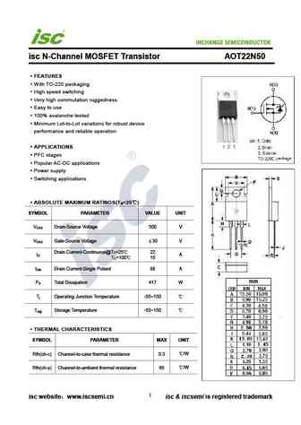
INCHANGE Semiconductor isc N-Channel MOSFET Transistor AOT22N50 FEATURES With TO-220 packaging High speed switching Very high commutation ruggedness Easy to use 100% avalanche tested Minimum Lot-to-Lot variations for robust device performance and reliable operation APPLICATIONS PFC stages Popular AC-DC applications Power supply Switching applications ABS
irfp32n50k.pdf
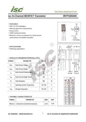
INCHANGE Semiconductor isc N-Channel MOSFET Transistor IRFP32N50K FEATURES With TO-247 packaging With low gate drive requirements Easy to drive 100% avalanche tested Minimum Lot-to-Lot variations for robust device performance and reliable operation APPLICATIONS Switching applications ABSOLUTE MAXIMUM RATINGS(T =25 ) a SYMBOL PARAMETER VALUE UNIT V Drain-Source
ixtq22n50p.pdf
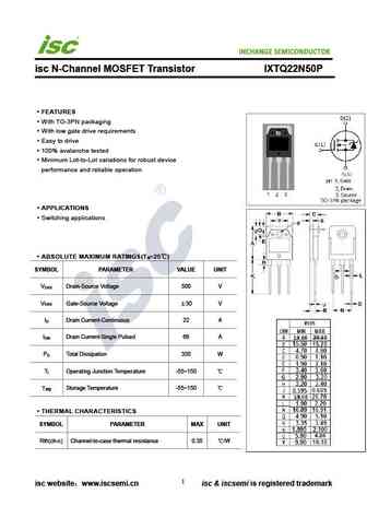
INCHANGE Semiconductor isc N-Channel MOSFET Transistor IXTQ22N50P FEATURES With TO-3PN packaging With low gate drive requirements Easy to drive 100% avalanche tested Minimum Lot-to-Lot variations for robust device performance and reliable operation APPLICATIONS Switching applications ABSOLUTE MAXIMUM RATINGS(T =25 ) a SYMBOL PARAMETER VALUE UNIT V Drain-Source
aob12n50.pdf
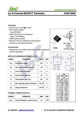
isc N-Channel MOSFET Transistor AOB12N50 FEATURES Drain Current I =12A@ T =25 D C Drain Source Voltage- V =500V(Min) DSS Static Drain-Source On-Resistance R = 0.52 (Max) DS(on) 100% avalanche tested Minimum Lot-to-Lot variations for robust device performance and reliable operation DESCRIPTION Designed for use in switch mode power supplies and general purpos
spw12n50c3.pdf
isc N-Channel MOSFET Transistor SPW12N50C3 ISPW12N50C3 FEATURES Static drain-source on-resistance RDS(on) 380m Enhancement mode 100% avalanche tested Minimum Lot-to-Lot variations for robust device performance and reliable operation DESCRITION Improved Transconductance ABSOLUTE MAXIMUM RATINGS(T =25 ) a SYMBOL PARAMETER VALUE UNIT V Drain-Source Voltage 50
2n5038.pdf
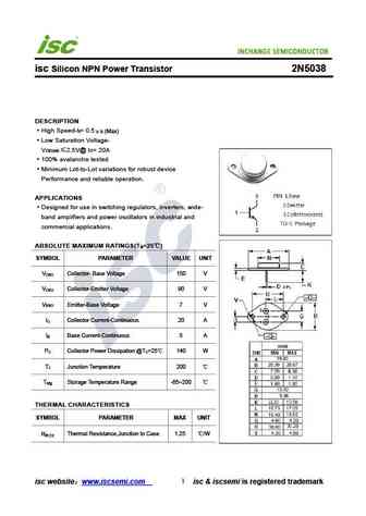
INCHANGE Semiconductor isc Silicon NPN Power Transistor 2N5038 DESCRIPTION High Speed-t = 0.5 s (Max) f Low Saturation Voltage- V 2.5V@ I = 20A CE(sat) C 100% avalanche tested Minimum Lot-to-Lot variations for robust device Performance and reliable operation. APPLICATIONS Designed for use in switching regulators, inverters, wide- band amplifiers and power oscillators
Другие IGBT... UF830, UF830Z, UF840, UK3568, UF450, UF460, 1N50, 1N50Z, 2SK3878, 3N50, 3N50Z, 4N50, 5N50, 5N50K, 6N50, 7N50, 8N50
Параметры MOSFET. Взаимосвязь и компромиссы
🌐 : EN ES РУ

Список транзисторов
Обновления
MOSFET: CS95118 | CS85105A | CS75N45 | CS72N12 | CS55N50 | CS48N75A | CS40N27 | MSQ60P04D | MSQ40P07D | MSQ30P40D | MSQ30P15 | MSQ30P07D | MSQ100N03D | MSHM60P14 | MSHM40N085 | MSHM30N46
Popular searches
bf494 | 2sc1885 | skd502t | 2sb754 | 2sc2362 | 2sd468 | c2240 transistor | 2sc1918