15N06. Аналоги и основные параметры
Наименование производителя: 15N06
Тип транзистора: MOSFET
Полярность: N
Предельные значения
Pd ⓘ - Максимальная рассеиваемая мощность: 2.2 W
|Vds|ⓘ - Максимально допустимое напряжение сток-исток: 60 V
|Vgs|ⓘ - Максимально допустимое напряжение затвор-исток: 15 V
|Id| ⓘ - Максимально допустимый постоянный ток стока: 15 A
Tj ⓘ - Максимальная температура канала: 175 °C
Электрические характеристики
tr ⓘ - Время нарастания: 160 ns
Cossⓘ - Выходная емкость: 230 pf
RDSonⓘ - Сопротивление сток-исток открытого транзистора: 0.075 Ohm
Тип корпуса: TO-220 SOP-8 TO-252 TO-220F
Аналог (замена) для 15N06
- подборⓘ MOSFET транзистора по параметрам
15N06 даташит
15n06.pdf
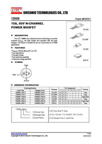
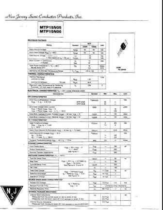
UNISONIC TECHNOLOGIES CO., LTD 15N06 Power MOSFET 15A, 60V N-CHANNEL POWER MOSFET 1 TO-220 DESCRIPTION 1 The UTC 15N06 uses advanced trench technology to provide TO-220F excellent RDS(ON), low gate charge and operation with low gate voltages. This device is suitable for use as a load switch or in PWM applications. 1 FEATURES TO-252 * RDS(ON)
15n06.pdf
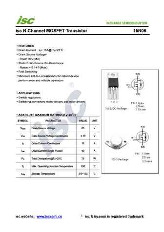
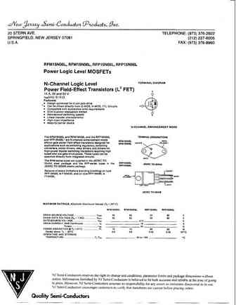
isc N-Channel MOSFET Transistor 15N06 FEATURES Drain Current I = 15A@ T =25 D C Drain Source Voltage- V = 60V(Min) DSS Static Drain-Source On-Resistance R = 0.14 (Max) DS(on) Fast Switching Minimum Lot-to-Lot variations for robust device performance and reliable operation APPLICATIONS Switch regulators Switching converters motor drivers and relay drivers
std15n06l std15n06l-1 std15n06lt4.pdf
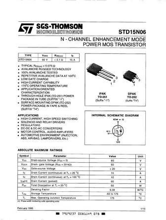
STD15N06L N - CHANNEL ENHANCEMENT MODE LOW THRESHOLD POWER MOS TRANSISTOR TYPE V R I DSS DS(on) D STD15N06L 60 V
mtd15n06vl.pdf
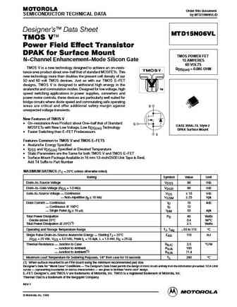
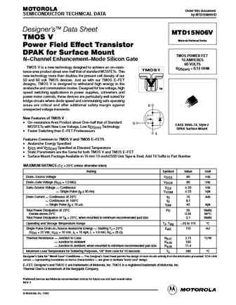
MOTOROLA Order this document SEMICONDUCTOR TECHNICAL DATA by MTD15N06VL/D Designer's Data Sheet MTD15N06VL TMOS V Power Field Effect Transistor DPAK for Surface Mount TMOS POWER FET N Channel Enhancement Mode Silicon Gate 15 AMPERES 60 VOLTS TMOS V is a new technology designed to achieve an on resis- RDS(on) = 0.085 OHM tance area product about one half that of sta
mtp15n06vl.pdf
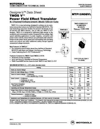
MOTOROLA Order this document SEMICONDUCTOR TECHNICAL DATA by MTP15N06VL/D Designer's Data Sheet MTP15N06VL TMOS V Power Field Effect Transistor N Channel Enhancement Mode Silicon Gate TMOS POWER FET TMOS V is a new technology designed to achieve an on resis- 15 AMPERES tance area product about one half that of standard MOSFETs. This 60 VOLTS new technology more tha
mtb15n06e.pdf

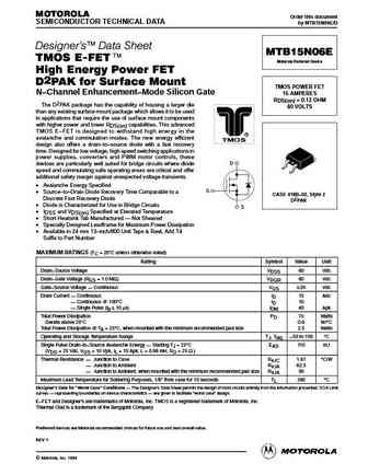
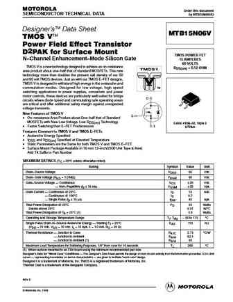
MOTOROLA Order this document SEMICONDUCTOR TECHNICAL DATA by MTB15N06E/D Designer's Data Sheet MTB15N06E TMOS E-FET. Motorola Preferred Device High Energy Power FET D2PAK for Surface Mount TMOS POWER FET N Channel Enhancement Mode Silicon Gate 15 AMPERES RDS(on) = 0.12 OHM The D2PAK package has the capability of housing a larger die 60 VOLTS than any existing surface mo
mtd15n06vlrev2.pdf

MOTOROLA Order this document SEMICONDUCTOR TECHNICAL DATA by MTD15N06VL/D Designer's Data Sheet MTD15N06VL TMOS V Power Field Effect Transistor DPAK for Surface Mount TMOS POWER FET N Channel Enhancement Mode Silicon Gate 15 AMPERES 60 VOLTS TMOS V is a new technology designed to achieve an on resis- RDS(on) = 0.085 OHM tance area product about one half that of sta
mtb15n06erev1.pdf
MOTOROLA Order this document SEMICONDUCTOR TECHNICAL DATA by MTB15N06E/D Designer's Data Sheet MTB15N06E TMOS E-FET. Motorola Preferred Device High Energy Power FET D2PAK for Surface Mount TMOS POWER FET N Channel Enhancement Mode Silicon Gate 15 AMPERES RDS(on) = 0.12 OHM The D2PAK package has the capability of housing a larger die 60 VOLTS than any existing surface mo
mtp15n06v.pdf
MOTOROLA Order this document SEMICONDUCTOR TECHNICAL DATA by MTP15N06V Designer's Data Sheet MTP15N06V TMOS V Motorola Preferred Device Power Field Effect Transistor N Channel Enhancement Mode Silicon Gate TMOS POWER FET TMOS V is a new technology designed to achieve an on resis- 15 AMPERES tance area product about one half that of standard MOSFETs. This 60 VOLTS new
mtd15n06v.pdf
MOTOROLA Order this document SEMICONDUCTOR TECHNICAL DATA by MTD15N06V/D Designer's Data Sheet MTD15N06V TMOS V Motorola Preferred Device Power Field Effect Transistor DPAK for Surface Mount TMOS POWER FET N Channel Enhancement Mode Silicon Gate 15 AMPERES 60 VOLTS TMOS V is a new technology designed to achieve an on resis- RDS(on) = 0.12 OHM tance area product about o
mtb15n06v.pdf
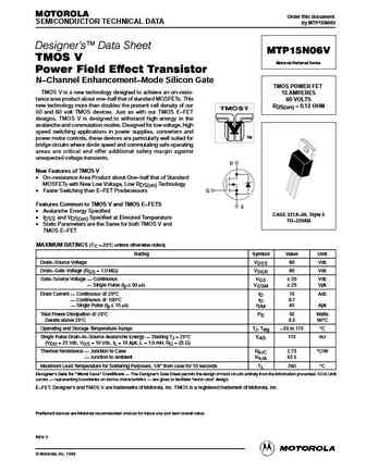
MOTOROLA Order this document SEMICONDUCTOR TECHNICAL DATA by MTB15N06V/D Designer's Data Sheet MTB15N06V TMOS V Power Field Effect Transistor D2PAK for Surface Mount TMOS POWER FET N Channel Enhancement Mode Silicon Gate 15 AMPERES 60 VOLTS TMOS V is a new technology designed to achieve an on resistance RDS(on) = 0.12 OHM area product about one half that of standard
phx15n06e 1.pdf
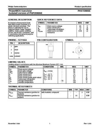
Philips Semiconductors Product specification PowerMOS transistor PHX15N06E Isolated version of PHP20N06E GENERAL DESCRIPTION QUICK REFERENCE DATA N-channel enhancement mode SYMBOL PARAMETER MAX. UNIT field-effect power transistor in a plastic full-pack envelope. The VDS Drain-source voltage 60 V device is intended for use in ID Drain current (DC) 13 A Switched Mode Power Supplies Pto
php15n06e 1.pdf
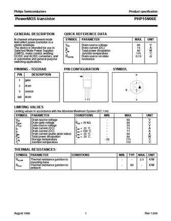
Philips Semiconductors Product specification PowerMOS transistor PHP15N06E GENERAL DESCRIPTION QUICK REFERENCE DATA N-channel enhancement mode SYMBOL PARAMETER MAX. UNIT field-effect power transistor in a plastic envelope. VDS Drain-source voltage 60 V The device is intended for use in ID Drain current (DC) 15 A Switched Mode Power Supplies Ptot Total power dissipation 60 W (SMPS), mo
std15n06-.pdf
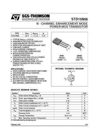
STD15N06 N - CHANNEL ENHANCEMENT MODE POWER MOS TRANSISTOR TYPE V R I DSS DS(on) D STD15N06 60 V
stp15n06l.pdf
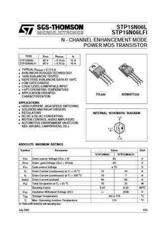
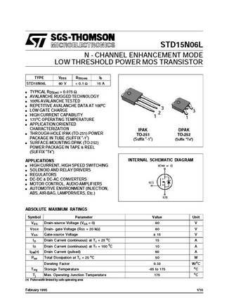
STP15N06L STP15N06LFI N - CHANNEL ENHANCEMENT MODE POWER MOS TRANSISTOR TYPE VDSS RDS(on) ID STP15N06L 60 V
stp15n06.pdf
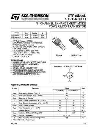
STP15N06L STP15N06LFI N - CHANNEL ENHANCEMENT MODE POWER MOS TRANSISTOR TYPE V R I DSS DS(on) D STP15N06L 60 V
fdmc15n06.pdf
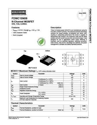
July 2009 FDMC15N06 N-Channel MOSFET 55V, 15A, 0.090 Features Description RDS(on) = 0.075 ( Typ.)@ VGS = 10V, ID = 15A These N-Channel power MOSFETs are manufactured using the innovative UItraFET process. This advanced process technology 100% Avalanche Tested achieves the lowest possible on-resistance per silicon area, resulting in outstanding performance.This device
rsq015n06tr.pdf
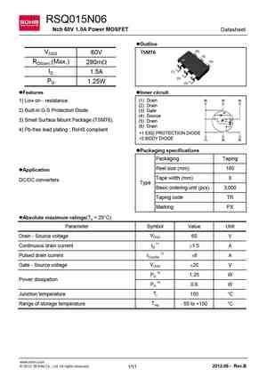
RSQ015N06 Nch 60V 1.5A Power MOSFET Datasheet lOutline (6) VDSS TSMT6 60V (5) (4) RDS(on) (Max.) 290mW (1) ID 1.5A (2) PD 1.25W (3) lFeatures lInner circuit (1) Drain 1) Low on - resistance. (2) Drain 2) Built-in G-S Protection Diode. (3) Gate (4) Source 3) Small Surface Mount Package (TSMT6). (5) Drain (6) Drain 4) Pb-free lead plating ; RoHS compliant
rsq015n06.pdf
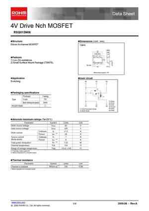
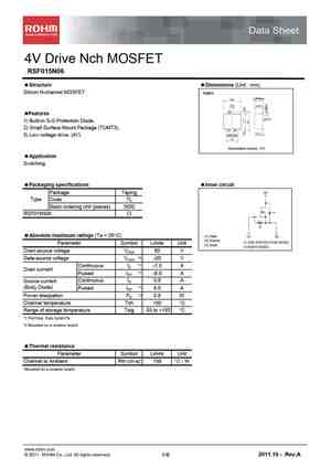
4V Drive Nch MOSFET RSQ015N06 Structure Dimensions (Unit mm) Silicon N-channel MOSFET TSMT6 1.0MAX 2.9 0.85 1.9 0.95 0.95 0.7 (6) (5) (4) Features 1) Low On-resistance. 0 0.1 2) Small Surface Mount Package (TSMT6). (1) (2) (3) 1pin mark 0.16 0.4 Abbreviated symbol PX Application Inner circuit Switching (6) (5) (4) 2 Packaging specifications Package T
rsf015n06.pdf
Data Sheet 4V Drive Nch MOSFET RSF015N06 Structure Dimensions (Unit mm) Silicon N-channel MOSFET TUMT3 Features 1) Built-in G-S Protection Diode. 2) Small Surface Mount Package (TUMT3). 3) Low voltage drive. (4V) Abbreviated symbol PX Application Switching Packaging specifications Inner circuit (3) Package Taping Type Code TL Basic ordering unit (p
sud15n06-90l.pdf
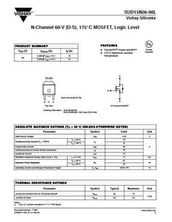
SUD15N06-90L Vishay Siliconix N-Channel 60-V (D-S), 175_C MOSFET, Logic Level FEATURES PRODUCT SUMMARY Pb-free D TrenchFETr Power MOSFET VDS (V) rDS(on) (W) ID (A) Available D 175_C Maximum Junction 0.065 @ VGS = 10 V 15 Temperature 60 60 0.090 @ VGS = 4.5 V 14 D TO-252 G Drain Connected to Tab S G D S Top View N-Channel MOSFET Ordering Information SUD15N06-90L SUD15N06-9
sqd15n06-42l.pdf
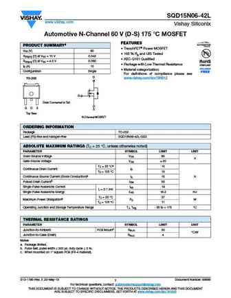
SQD15N06-42L www.vishay.com Vishay Siliconix Automotive N-Channel 60 V (D-S) 175 C MOSFET FEATURES PRODUCT SUMMARYd TrenchFET Power MOSFET VDS (V) 60 100 % Rg and UIS Tested RDS(on) ( ) at VGS = 10 V 0.042 AEC-Q101 Qualified RDS(on) ( ) at VGS = 4.5 V 0.060 Package with Low Thermal Resistance ID (A) 15 Material categorization Configuration Single
ipd15n06s2l-64.pdf
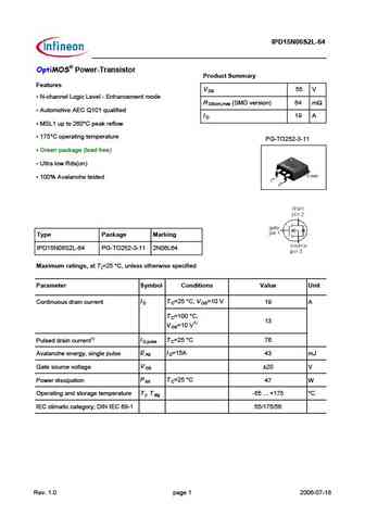
IPD15N06S2L-64 OptiMOS Power-Transistor Product Summary Features V 55 V DS N-channel Logic Level - Enhancement mode R (SMD version) 64 m DS(on),max Automotive AEC Q101 qualified I 19 A D MSL1 up to 260 C peak reflow 175 C operating temperature PG-TO252-3-11 Green package (lead free) Ultra low Rds(on) 100% Avalanche tested Type Package Markin
ntd15n06-001.pdf
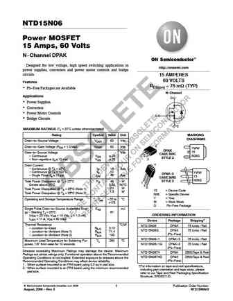
NTD15N06 Power MOSFET 15 Amps, 60 Volts N-Channel DPAK Designed for low voltage, high speed switching applications in http //onsemi.com power supplies, converters and power motor controls and bridge circuits. 15 AMPERES 60 VOLTS Features RDS(on) = 76 mW (TYP) Pb-Free Packages are Available N-Channel Applications D Power Supplies Converters Power Motor Controls
ntd15n06l-001.pdf

NTD15N06L Power MOSFET 15 Amps, 60 Volts, Logic Level N-Channel DPAK http //onsemi.com Designed for low voltage, high speed switching applications in 15 AMPERES power supplies, converters and power motor controls and bridge 60 VOLTS circuits. RDS(on) = 85 mW (TYP) Features N-Channel Pb-Free Packages are Available D Applications Power Supplies Converters G Po
rfd15n06le-sm.pdf
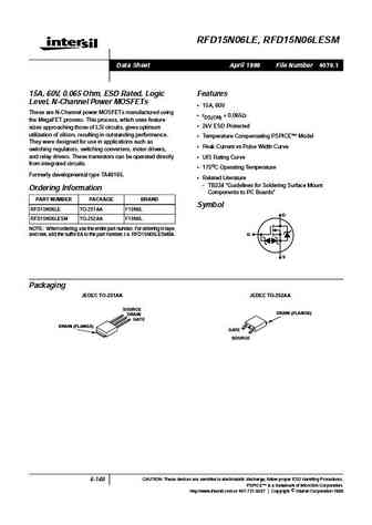
RFD15N06LE, RFD15N06LESM Data Sheet April 1999 File Number 4079.1 15A, 60V, 0.065 Ohm, ESD Rated, Logic Features Level, N-Channel Power MOSFETs 15A, 60V These are N-Channel power MOSFETs manufactured using rDS(ON) = 0.065 the MegaFET process. This process, which uses feature 2kV ESD Protected sizes approaching those of LSI circuits, gives optimum utilization of silicon,
rfp15n05l rfp15n06l.pdf
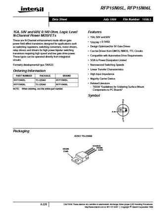
RFP15N05L, RFP15N06L Data Sheet July 1999 File Number 1558.3 15A, 50V and 60V, 0.140 Ohm, Logic Level Features N-Channel Power MOSFETs 15A, 50V and 60V These are N-Channel enhancement mode silicon gate rDS(ON) = 0.140 power field effect transistors designed for applications such Design Optimized for 5V Gate Drives as switching regulators, switching converters, motor driv
tt015n060eq.pdf
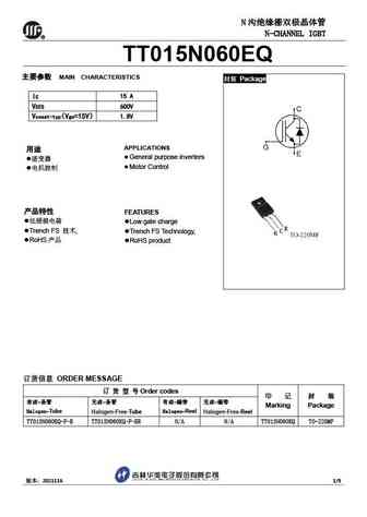
N N-CHANNEL IGBT R TT015N060EQ MAIN CHARACTERISTICS Package IC 15 A VCES 600V Vcesat-typ 1.8V Vge=15V APPLICATIONS General purpose inverters Motor Control FEATURES Low gate charge Trench FS , Trench FS Tec
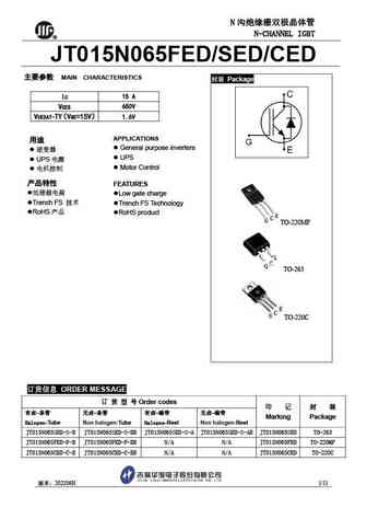
jt015n065fed.pdf
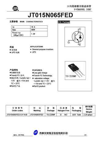
N N-CHANNEL IGBT R JT015N065FED MAIN CHARACTERISTICS Package IC 15 A VCES 650V Vcesat-typ 1.6V @Vge=15V APPLICATIONS General purpose inverters UPS UPS FEATURES Low gate charge Trench FS , Trench FS Technology,
hfp15n06.pdf
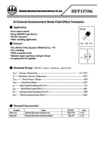
Shantou Huashan Electronic Devices Co.,Ltd. HFP15N06 N-Channel Enhancement Mode Field Effect Transistor Applications TO-220 Servo motor control. Power MOSFET gate drivers. DC/DC converters Other switching applications. 1- G 2-D 3-S Features 15A, 60V(See Note), RDS(on)
dhs015n06 dhs015n06e.pdf
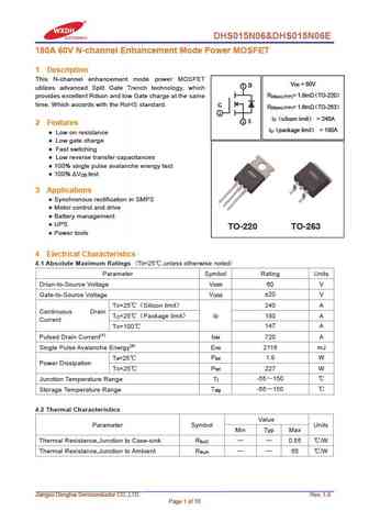
DHS015N06&DHS015N06E 180A 60V N-channel Enhancement Mode Power MOSFET 1 Description This N-channel enhancement mode power MOSFET V = 60V DS 2 D utilizes advanced Split Gate Trench technology, which R = 1.8m TO-220 DS(on) (TYP) provides excellent Rdson and low Gate charge at the same time. Which accords with the RoHS standard. G R = 1.6m TO-263 DS(on) (TYP) 1 I
dhd015n06.pdf
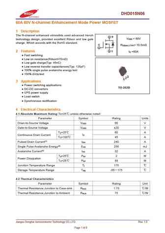
DHD015N06 60A 60V N-channel Enhancement Mode Power MOSFET 1 Description The N-channel enhanced vdmosfets used advanced trench 2 D V = 60V DSS technology design, provided excellent Rdson and low gate charge. Which accords with the RoHS standard. G R = 10.5m DS(on) (TYP) 1 3 S 2 Features I =60A D Fast switching Low on resistance(Rdson 15m ) Low gate charge(Typ
blqm15n06l-d.pdf
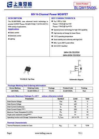
Green Product BLQM15N06L 60V N-Channel Power MOSFET DESCRIPTION KEY CHARACTERISTICS The BLQM15N06L uses advanced trench technology to V = 60V,I = DS D 50A R
swk15n06v.pdf
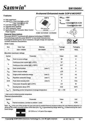
SW15N06V N-channel Enhanced mode SOP-8 MOSFET Features BVDSS 60V SOP-8 D High ruggedness D ID 15A D Low RDS(ON) (Typ 8.5m )@VGS=4.5V D RDS(ON) 8.5m @VGS=4.5V (Typ 7.5m )@VGS=10V G Low Gate Charge (Typ 79nC) S 7.5m @VGS=10V S Improved dv/dt Capability S 100% Avalanche Tested G(4) D(5,6,7,8) D Application DC
sre15n065fsudj.pdf
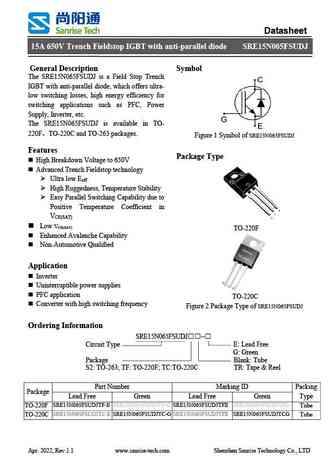
Datasheet 15A 650V Trench Fieldstop IGBT with anti-parallel diode SRE15N065FSUDJ General Description Symbol The SRE15N065FSUDJ is a Field Stop Trench IGBT with anti-parallel diode, which offers ultra- low switching losses, high energy efficiency for switching applications such as PFC, Power Supply, Inverter, etc. The SRE15N065FSUDJ is available in TO- 220F TO-220C and TO-263
sre15n060fsude.pdf
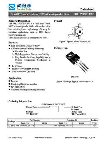
Datasheet 15A 600V Trench Fieldstop IGBT with anti-parallel diode SRE15N060FSUDE General Description Symbol The SRE15N060FSUDE is a Field Stop Trench IGBT with anti-parallel diode, which offers ultra- low switching losses, high energy efficiency for switching applications such as PFC, Power Supply, Inverter, etc. The SRE15N060FSUDE package is TO-220F. Figure 1 Symbol of SRE15N0
dac015n065z2.pdf
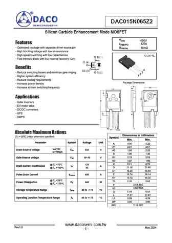
DAC015N065Z2 Silicon Carbide Enhancement Mode MOSFET VDSS 650V Features I 120A D(@25 ) RDS(ON) 15m TO-247-4L Benefits
tsb15n06a.pdf

TSB15N06A Wuxi Unigroup Microelectronics Company 60V N-Channel DTMOS FEATURES Trench Power DTMOS Technology Low RDS(ON) Low Gate Charge Optimized for fast-switching Applications APPLICATIONS Synchronous Rectification in DC/DC and AC/DC Converters Isolated DC/DC Converters in Telecom and Industrial Device Marking and Package Information Device Pac
tsp15n06a.pdf
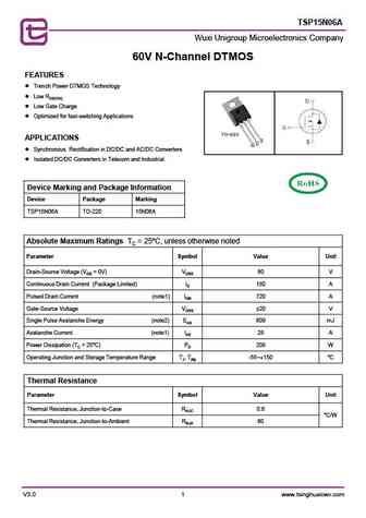
TSP15N06A Wuxi Unigroup Microelectronics Company 60V N-Channel DTMOS FEATURES Trench Power DTMOS Technology Low RDS(ON) Low Gate Charge Optimized for fast-switching Applications APPLICATIONS Synchronous Rectification in DC/DC and AC/DC Converters Isolated DC/DC Converters in Telecom and Industrial Device Marking and Package Information Device Pac
fxn15n06d.pdf
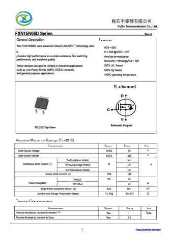
FuXin Semiconductor Co., Ltd. FXN15N06D Series Rev.A General Description Features The FXN15N06D uses advanced Silicon s MOSFET Technology, whic VDS = 60V h ID = 45A @VGS = 10V provides high performance in on-state resistance, fast switching Very low on-resistance performance, and excellent quality. RDS(ON)
ipd15n06s2l64.pdf
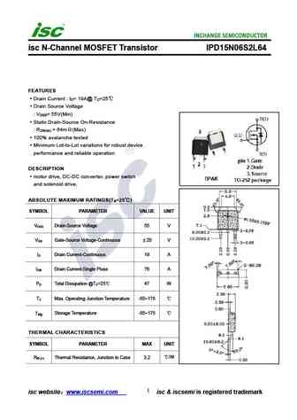
isc N-Channel MOSFET Transistor IPD15N06S2L64 FEATURES Drain Current I = 19A@ T =25 D C Drain Source Voltage V = 55V(Min) DSS Static Drain-Source On-Resistance R = 64m (Max) DS(on) 100% avalanche tested Minimum Lot-to-Lot variations for robust device performance and reliable operation DESCRIPTION motor drive, DC-DC converter, power switch and solenoid drive.
ap15n06s.pdf
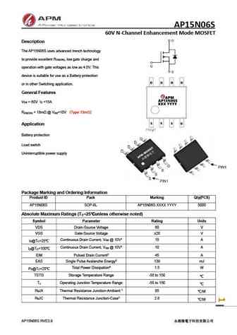
AP15N06S 60V N-Channel Enhancement Mode MOSFET Description The AP15N06S uses advanced trench technology to provide excellent R , low gate charge and DS(ON) operation with gate voltages as low as 4.5V. This device is suitable for use as a Battery protection or in other Switching application. General Features V = 60V I =15A DS D R
Другие IGBT... 2N7000Z, 2N7002LL, 2N7002Z, 2N7002ZT, UF3055, UTD3055, 12N06, 12N06Z, STP65NF06, 12N10, 15N20, 19N10, 22N20, 25N06, 25N10, 30N06, 50N06
🌐 : EN ES РУ

Список транзисторов
Обновления
MOSFET: AUW033N08BG | AUW025N10 | AUR030N10 | AUR020N10 | AUR020N085 | AUR014N10 | AUP074N10 | AUP065N10 | AUP062N08BG | AUP060N08AG | HYG053N10NS1B | HYG053N10NS1P | AP220N04T | AP220N04P | QM3126M3 | AUP060N055
Popular searches
2sc1451 | c3199 transistor | 2n2712 datasheet | 2sc2525 | tip73 | 2n3392 | 2n2369a | 2sc733