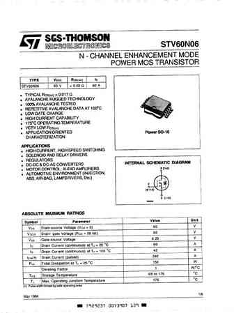
60N06 datasheet, аналоги, основные параметры
Наименование производителя: 60N06 📄📄
Тип транзистора: MOSFET
Полярность: N
Предельные значения
Pd ⓘ - Максимальная рассеиваемая мощность: 100 W
|Vds|ⓘ - Максимально допустимое напряжение сток-исток: 60 V
|Vgs|ⓘ - Максимально допустимое напряжение затвор-исток: 20 V
|Id| ⓘ - Максимально допустимый постоянный ток стока: 60 A
Tj ⓘ - Максимальная температура канала: 150 °C
Электрические характеристики
tr ⓘ - Время нарастания: 11 ns
Cossⓘ - Выходная емкость: 400 pf
RDSonⓘ - Сопротивление сток-исток открытого транзистора: 0.014 Ohm
📄📄 Копировать
Аналог (замена) для 60N06
- подборⓘ MOSFET транзистора по параметрам
60N06 даташит
60n06.pdf
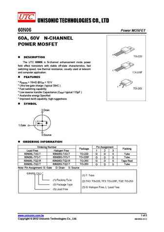
UNISONIC TECHNOLOGIES CO., LTD 60N06 Power MOSFET 60A, 60V N-CHANNEL POWER MOSFET DESCRIPTION The UTC 60N06 is N-channel enhancement mode power field effect transistors with stable off-state characteristics, fast switching speed, low thermal resistance, usually used at telecom and computer application. FEATURES * RDS(ON) = 18m @VGS = 10 V * Ultra low gate charge (
60n06.pdf
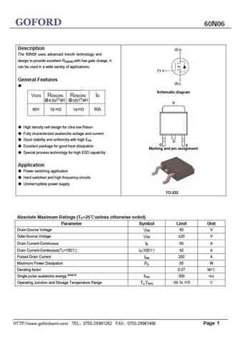
GOFORD 60N06 Description The NCE6050KA advanced trench technology and The 60N06 uses uses advanced trench technology and design to provide excellent RDS(ON) with low gate charge. It can be used in a wide variety of applications. General Features Schematic diagram VDSS RDS(ON) RDS(ON) ID @ 4.5V (Typ) @10V (Typ) 60V m 18 14m 60A High density cell design fo
60n06.pdf
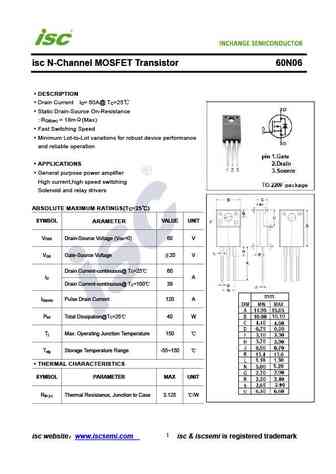
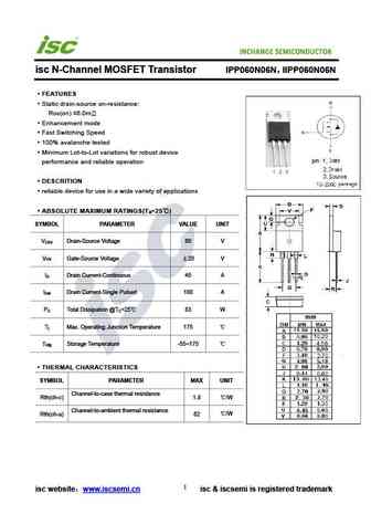
INCHANGE Semiconductor isc N-Channel MOSFET Transistor 60N06 DESCRIPTION Drain Current I = 60A@ T =25 D C Static Drain-Source On-Resistance R = 18m (Max) DS(on) Fast Switching Speed Minimum Lot-to-Lot variations for robust device performance and reliable operation APPLICATIONS General purpose power amplifier High current,high speed switching Solenoid and relay
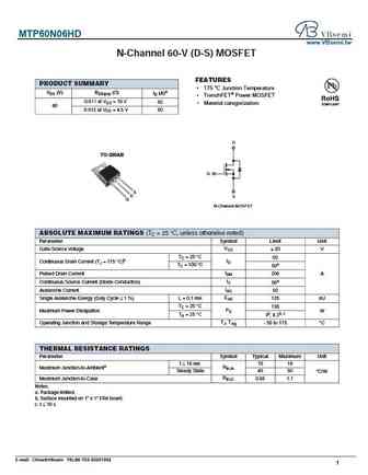
mtp60n06hd.pdf
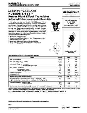
MOTOROLA Order this document SEMICONDUCTOR TECHNICAL DATA by MTP60N06HD/D Designer's Data Sheet MTP60N06HD HDTMOS E-FET. Motorola Preferred Device Power Field Effect Transistor N Channel Enhancement Mode Silicon Gate TMOS POWER FET This advanced high cell density HDTMOS power FET is 60 AMPERES designed to withstand high energy in the avalanche and commuta- 60 VOLTS tio
mtb60n06hd.pdf
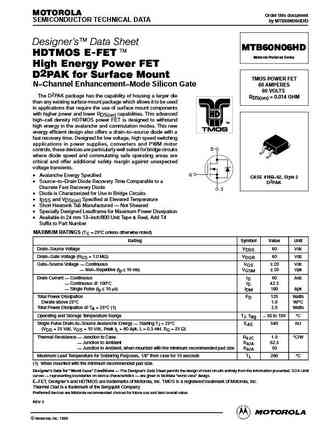
MOTOROLA Order this document SEMICONDUCTOR TECHNICAL DATA by MTB60N06HD/D Designer's Data Sheet MTB60N06HD HDTMOS E-FET. Motorola Preferred Device High Energy Power FET D2PAK for Surface Mount TMOS POWER FET 60 AMPERES N Channel Enhancement Mode Silicon Gate 60 VOLTS The D2PAK package has the capability of housing a larger die RDS(on) = 0.014 OHM than any existing sur
mtb60n06hdrev2x.pdf

MOTOROLA Order this document SEMICONDUCTOR TECHNICAL DATA by MTB60N06HD/D Designer's Data Sheet MTB60N06HD HDTMOS E-FET. Motorola Preferred Device High Energy Power FET D2PAK for Surface Mount TMOS POWER FET 60 AMPERES N Channel Enhancement Mode Silicon Gate 60 VOLTS The D2PAK package has the capability of housing a larger die RDS(on) = 0.014 OHM than any existing sur
php60n06t 1.pdf
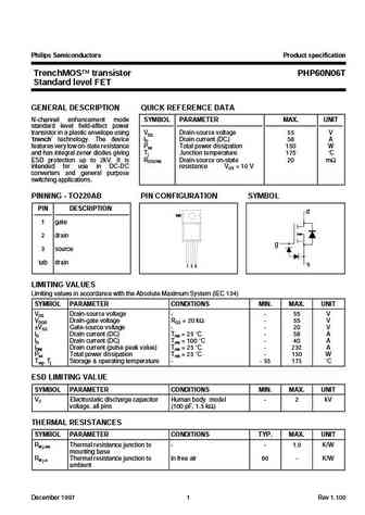
Philips Semiconductors Product specification TrenchMOS transistor PHP60N06T Standard level FET GENERAL DESCRIPTION QUICK REFERENCE DATA N-channel enhancement mode SYMBOL PARAMETER MAX. UNIT standard level field-effect power transistor in a plastic envelope using VDS Drain-source voltage 55 V trench technology. The device ID Drain current (DC) 58 A features very low on-state r
php60n06lt 2.pdf

Philips Semiconductors Product specification TrenchMOS transistor PHP60N06LT, PHB60N06LT Logic level FET FEATURES SYMBOL QUICK REFERENCE DATA Trench technology VDSS = 55 V d Very low on-state resistance Fast switching ID = 58 A Stable off-state characteristics High thermal cycling performance RDS(ON) 20 m (VGS = 5 V) g Low thermal resistance
phb60n06t 1.pdf
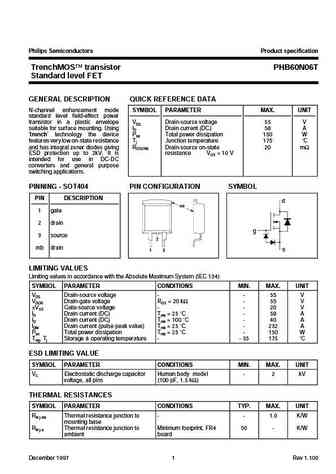
Philips Semiconductors Product specification TrenchMOS transistor PHB60N06T Standard level FET GENERAL DESCRIPTION QUICK REFERENCE DATA N-channel enhancement mode SYMBOL PARAMETER MAX. UNIT standard level field-effect power transistor in a plastic envelope VDS Drain-source voltage 55 V suitable for surface mounting. Using ID Drain current (DC) 58 A trench technology the devic
php60n06lt phb60n06lt.pdf
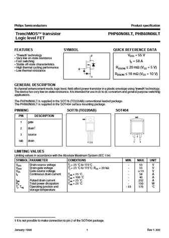
Philips Semiconductors Product specification TrenchMOS transistor PHP60N06LT, PHB60N06LT Logic level FET FEATURES SYMBOL QUICK REFERENCE DATA Trench technology VDSS = 55 V d Very low on-state resistance Fast switching ID = 58 A Stable off-state characteristics High thermal cycling performance RDS(ON) 20 m (VGS = 5 V) g Low thermal resistance
stp60n05 stp60n06.pdf

STP60N05-14 STP60N06-14 N - CHANNEL ENHANCEMENT MODE POWER MOS TRANSISTOR PRELIMINARY DATA TYPE V R I DSS DS(on) D STP60N05-14 50 V
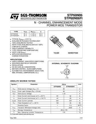
stp60n05-14 stp60n06-14.pdf
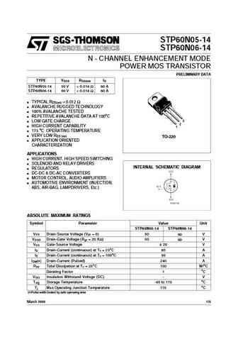
STP60N05-14 STP60N06-14 N - CHANNEL ENHANCEMENT MODE POWER MOS TRANSISTOR PRELIMINARY DATA TYPE V R I DSS DS(on) D STP60N05-14 50 V
stp60n05-16 stp60n06-16.pdf
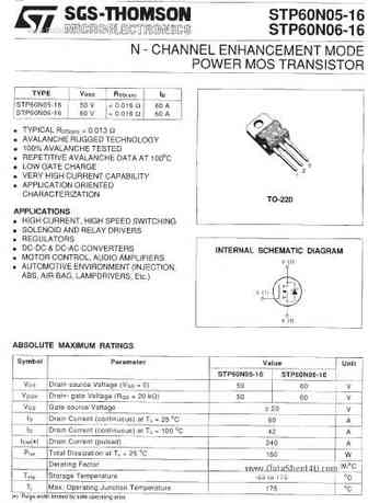
www.DataSheet4U.com www.DataSheet4U.com www.DataSheet4U.com www.DataSheet4U.com www.DataSheet4U.com www.DataSheet4U.com www.DataSheet4U.com
stb60n06-14.pdf
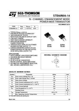
STB60N06-14 N - CHANNEL ENHANCEMENT MODE POWER MOS TRANSISTOR PRELIMINARY DATA TYPE V R I DSS DS(on) D STB60N06-14 60 V

sqm60n06-15.pdf
SQM60N06-15 www.vishay.com Vishay Siliconix Automotive N-Channel 60 V (D-S) 175 C MOSFET FEATURES PRODUCT SUMMARY Halogen-free According to IEC 61249-2-21 VDS (V) 60 Definition RDS(on) ( ) at VGS = 10 V 0.015 TrenchFET Power MOSFET ID (A) 56 Package with Low Thermal Resistance AEC-Q101 Qualifiedd Configuration Single 100 % Rg and UIS Tested D Charac
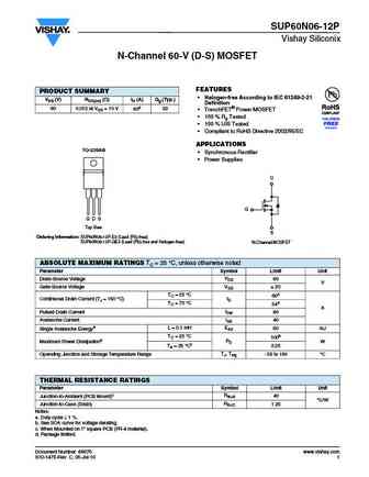
sup60n06-18 sub60n06-18.pdf
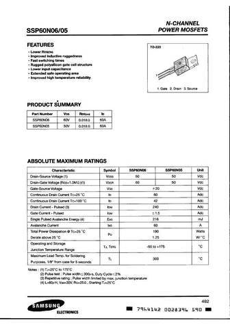
SUP/SUB60N06-18 Vishay Siliconix N-Channel 60-V (D-S), 175_C MOSFET PRODUCT SUMMARY V(BR)DSS (V) rDS(on) (W) ID (A) 60 0.018 60 TO-220AB D TO-263 DRAIN connected to TAB G G D S G D S Top View Top View S SUB60N06-18 SUP60N06-18 N-Channel MOSFET ABSOLUTE MAXIMUM RATINGS (TC = 25_C UNLESS OTHERWISE NOTED) Parameter Symbol Limit Unit Drain-Source Voltage VDS 60 V V Gate-Sourc
sqm60n06.pdf
SQM60N06-15 Vishay Siliconix Automotive N-Channel 60 V (D-S) 175 C MOSFET FEATURES PRODUCT SUMMARY Halogen-free According to IEC 61249-2-21 VDS (V) 60 Definition RDS(on) ( ) at VGS = 10 V 0.015 TrenchFET Power MOSFET ID (A) 56 Package with Low Thermal Resistance Configuration Single AEC-Q101 Qualifiedd Characterization Ongoing D Compliant to RoHS D
sqp60n06-15.pdf
SQP60N06-15 www.vishay.com Vishay Siliconix Automotive N-Channel 60 V (D-S) 175 C MOSFET FEATURES PRODUCT SUMMARY TrenchFET Power MOSFET VDS (V) 60 Package with Low Thermal Resistance RDS(on) ( ) at VGS = 10 V 0.015 AEC-Q101 Qualifiedd ID (A) 56 100 % Rg and UIS Tested Configuration Single Material categorization D TO-220AB For definitions of complianc
ipb260n06n3-g ipp260n06n3-g.pdf
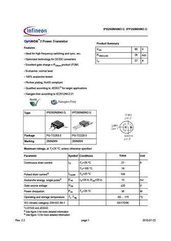
Type IPB260N06N3 G IPP260N06N3 G OptiMOS 3 Power-Transistor Product Summary Features V 60 V DS Ideal for high frequency switching and sync. rec. R 26 m DS(on),max Optimized technology for DC/DC converters I 27 A D Excellent gate charge x R product (FOM) DS(on) N-channel, normal level 100% avalanche tested Pb-free plating; RoHS compliant Qualifie
ipa060n06n.pdf
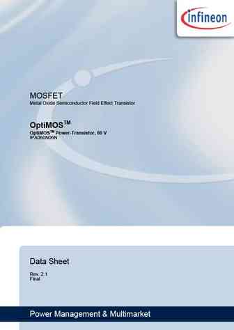
MOSFET Metal Oxide Semiconductor Field Effect Transistor OptiMOSTM OptiMOSTM Power-Transistor, 60 V IPA060N06N Data Sheet Rev. 2.1 Final Power Management & Multimarket OptiMOSTM Power-Transistor, 60 V IPA060N06N TO-220-FP 1 Description Features Optimized for high performance SMPS, e.g. sync. rec. 100% avalanche tested Superior thermal resistance N-channel
ipp060n06n.pdf
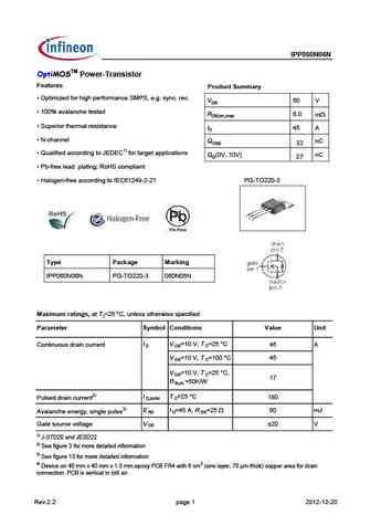
Type IPP060N06N OptiMOSTM Power-Transistor Features Product Summary Optimized for high performance SMPS, e.g. sync. rec. VDS 60 V 100% avalanche tested RDS(on),max 6.0 mW Superior thermal resistance ID 45 A N-channel QOSS nC 32 Qualified according to JEDEC1) for target applications QG(0V..10V) nC 27 Pb-free lead plating; RoHS compliant Hal
ipa060n06nm5s.pdf
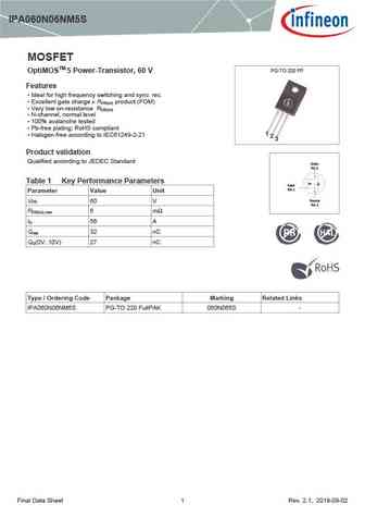
IPA060N06NM5S MOSFET PG-TO 220 FP OptiMOSTM 5 Power-Transistor, 60 V Features Ideal for high frequency switching and sync. rec. Excellent gate charge x R product (FOM) DS(on) Very low on-resistance R DS(on) N-channel, normal level 100% avalanche tested Pb-free plating; RoHS compliant Halogen-free according to IEC61249-2-21 Product validation Qualified
om60n06sa.pdf
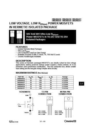
OM60N06SA OM60N05SA OM50N06ST OM50N06SA OM50N05SA OM50N05ST LOW VOLTAGE, LOW RDS(on) POWER MOSFETS IN HERMETIC ISOLATED PACKAGE 50V And 60V Ultra Low RDS(on) Power MOSFETs In TO-257 And TO-254 Isolated Packages FEATURES Isolated Hermetic Metal Packages Ultra Low RDS(on) Low Conductive Loss/Low Gate Charge Available Screened To MIL-S-19500, TX, TXV And S Levels Ce
ntb60n06l ntp60n06l ntp60n06l ntb60n06l.pdf
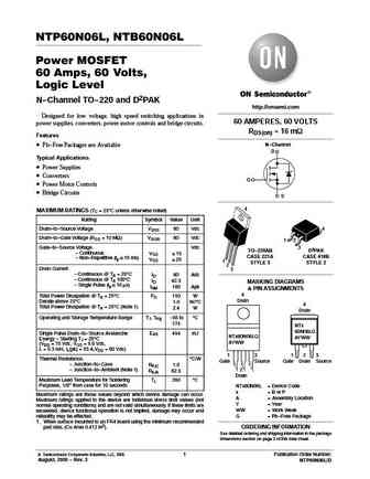
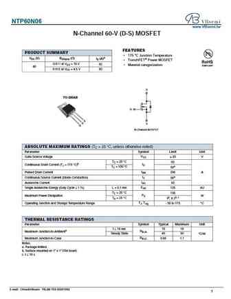
NTP60N06L, NTB60N06L Power MOSFET 60 Amps, 60 Volts, Logic Level N-Channel TO-220 and D2PAK http //onsemi.com Designed for low voltage, high speed switching applications in 60 AMPERES, 60 VOLTS power supplies, converters, power motor controls and bridge circuits. RDS(on) = 16 mW Features N-Channel Pb-Free Packages are Available D Typical Applications Power Supplies C
ntb60n06g ntp60n06 ntp60n06 ntb60n06.pdf
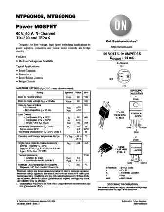
NTP60N06, NTB60N06 Power MOSFET 60 V, 60 A, N-Channel TO-220 and D2PAK Designed for low voltage, high speed switching applications in http //onsemi.com power supplies, converters and power motor controls and bridge circuits. 60 VOLTS, 60 AMPERES Features RDS(on) = 14 mW Pb-Free Packages are Available N-Channel D Typical Applications Power Supplies Converters Pow
nvb60n06.pdf
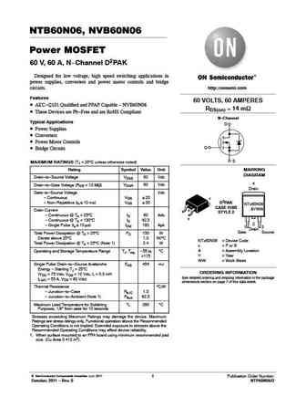
NTB60N06, NVB60N06 Power MOSFET 60 V, 60 A, N-Channel D2PAK Designed for low voltage, high speed switching applications in power supplies, converters and power motor controls and bridge circuits. http //onsemi.com Features 60 VOLTS, 60 AMPERES AEC-Q101 Qualified and PPAP Capable - NVB60N06 RDS(on) = 14 mW These Devices are Pb-Free and are RoHS Compliant N-Channel Typical App
60n06l-ta3-t 60n06g-ta3-t 60n06l-tf3-t 60n06g-tf3-t 60n06l-tq2-r 60n06g-tq2-r 60n06l-tq2-t 60n06g-tq2-t.pdf

UNISONIC TECHNOLOGIES CO., LTD 60N06 Power MOSFET 60A, 60V N-CHANNEL POWER MOSFET DESCRIPTION The UTC 60N06 is N-channel enhancement mode power field effect transistors with stable off-state characteristics, fast switching speed, low thermal resistance, usually used at telecom and computer application. FEATURES * RDS(ON) = 18m @VGS = 10 V * Ultra low gate charge (
utt60n06.pdf
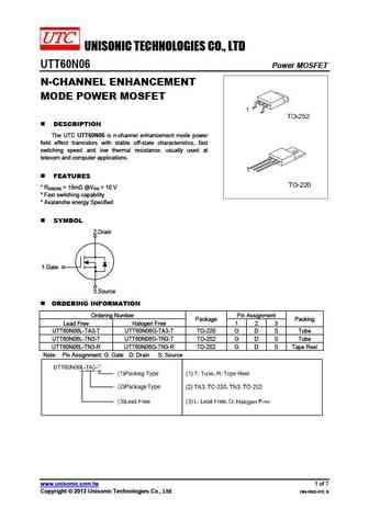
UNISONIC TECHNOLOGIES CO., LTD UTT60N06 Power MOSFET N-CHANNEL ENHANCEMENT MODE POWER MOSFET DESCRIPTION The UTC UTT60N06 is n-channel enhancement mode power field effect transistors with stable off-state characteristics, fast switching speed and low thermal resistance. usually used at telecom and computer applications. FEATURES * RDS(ON) = 18m @VGS = 10 V * Fast s
tsm60n06cp.pdf
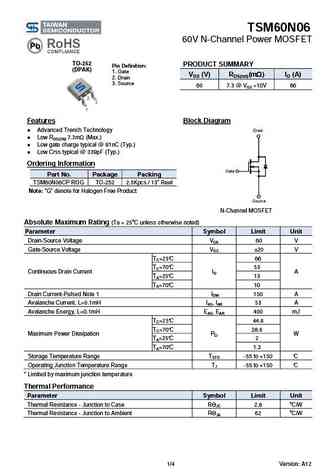
TSM60N06 60V N-Channel Power MOSFET TO-252 PRODUCT SUMMARY Pin Definition (DPAK) 1. Gate VDS (V) RDS(on)(m ) ID (A) 2. Drain 3. Source 60 7.3 @ VGS =10V 66 Features Block Diagram Advanced Trench Technology Low RDS(ON) 7.3m (Max.) Low gate charge typical @ 81nC (Typ.) Low Crss typical @ 339pF (Typ.) Ordering Information Part No. Packag
kf60n06p.pdf
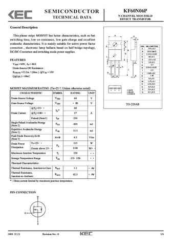
KF60N06P SEMICONDUCTOR N CHANNEL MOS FIELD TECHNICAL DATA EFFECT TRANSISTOR General Description A This planar stripe MOSFET has better characteristics, such as fast O C switching time, low on resistance, low gate charge and excellent F avalanche characteristics. It is mainly suitable for active power factor E DIM MILLIMETERS G correction , electronic lamp ballasts based on half
cep60n06g ceb60n06g.pdf
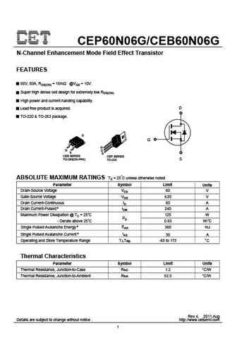
CEP60N06G/CEB60N06G N-Channel Enhancement Mode Field Effect Transistor FEATURES 60V, 60A, RDS(ON) = 16m @VGS = 10V. Super high dense cell design for extremely low RDS(ON). High power and current handing capability. D Lead free product is acquired. TO-220 & TO-263 package. G CEB SERIES CEP SERIES TO-263(DD-PAK) S TO-220 ABSOLUTE MAXIMUM RATINGS Tc = 25 C unless otherwise noted
gmp60n06.pdf
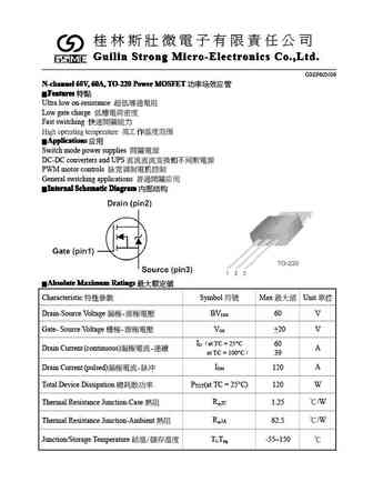
Guilin Strong Micro-Electronics Co.,Ltd. Guilin Strong Micro-Electronics Co.,Ltd. Guilin Strong Micro-Electronics Co.,Ltd. Guilin Strong Micro-Electronics Co.,Ltd. GMP60N06 N-channel 60V, 60A, TO-220 Power MOSFET N-channel 60V, 60A, TO-220 Power MOSFET N-channel 60V, 60A, TO-220 Power MOSFET N-channel 60V, 60A, TO-2
mtb60n06j3.pdf
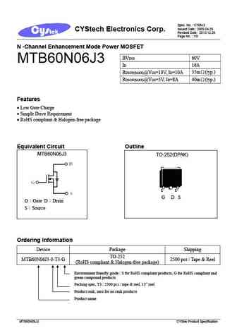
Spec. No. C708J3 Issued Date 2009.04.29 CYStech Electronics Corp. Revised Date 2013.12.26 Page No. 1/9 N -Channel Enhancement Mode Power MOSFET BVDSS 60V MTB60N06J3 ID 16A 35m (typ.) RDSON(MAX)@VGS=10V, ID=10A 40m (typ.) RDSON(MAX)@VGS=5V, ID=8A Features Low Gate Charge Simple Drive Requirement RoHS compliant & Halogen-free package Equivalen
mtb60n06l3.pdf
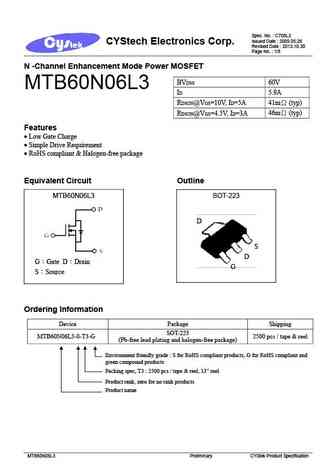
Spec. No. C708L3 Issued Date 2009.05.26 CYStech Electronics Corp. Revised Date 2013.10.30 Page No. 1/8 N -Channel Enhancement Mode Power MOSFET BVDSS 60V MTB60N06L3 ID 5.9A 41m (typ) RDSON@VGS=10V, ID=5A 46m (typ) RDSON@VGS=4.5V, ID=3A Features Low Gate Charge Simple Drive Requirement RoHS compliant & Halogen-free package Equivalent Circui
mtb060n06i3.pdf
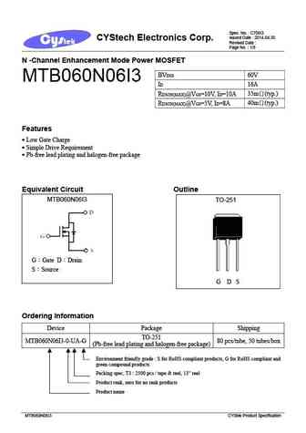
Spec. No. C708I3 Issued Date 2014.04.30 CYStech Electronics Corp. Revised Date Page No. 1/8 N -Channel Enhancement Mode Power MOSFET BVDSS 60V MTB060N06I3 ID 16A RDSON(MAX)@VGS=10V, ID=10A 35m (typ.) RDSON(MAX)@VGS=5V, ID=8A 40m (typ.) Features Low Gate Charge Simple Drive Requirement Pb-free lead plating and halogen-free package Equivalent Cir
hfp60n06.pdf
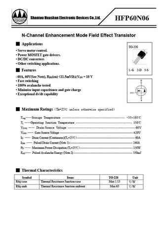
Shantou Huashan Electronic Devices Co.,Ltd. HFP60N06 N-Channel Enhancement Mode Field Effect Transistor Applications TO-220 Servo motor control. Power MOSFET gate drivers. DC/DC converters Other switching applications. 1- G 2-D 3-S Features 60A, 60V(See Note), RDS(on)
cs60n06 c4.pdf

Silicon N-Channel Power MOSFET R CS60N06 C4 General Description VDSS 60 V CS60N06 C4, the silicon N-channel Enhanced ID 55 A PD(TC=25 ) 150 W VDMOSFETs, is obtained by the self-aligned planar Technology RDS(ON)Typ 8 m which reduce the conduction loss, improve switching performance and enhance the avalanche energy. The transistor can be used in various power
dh60n06.pdf
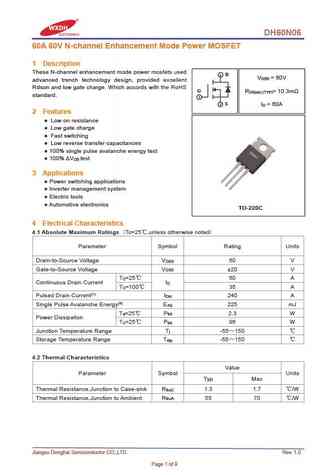
DH60N06 60A 60V N-channel Enhancement Mode Power MOSFET 1 Description These N-channel enhancement mode power mosfets used 2 D V = 60V DSS advanced trench technology design, provided excellent Rdson and low gate charge. Which accords with the RoHS G R = 10.3m DS(on) (TYP) standard. 1 3 S I = 60A D 2 Features Low on resistance Low gate charge Fast switching
fhp60n06b.pdf
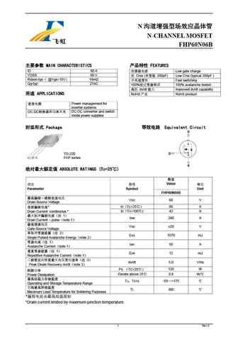
N N-CHANNEL MOSFET FHP60N06B MAIN CHARACTERISTICS FEATURES ID 60 A Low gate charge VDSS 60 V Crss ( 200pF) Low Crss (typical 200pF ) Rdson-typ @Vgs=10V 18m Fast switching Qg-typ 27nC 100% 100% avalanche tested dv/dt Improved dv
sre60n065fsud6.pdf
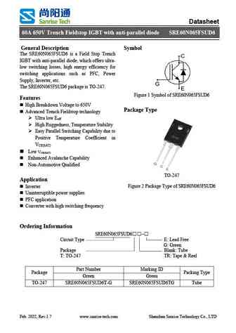
Datasheet 60A 650V Trench Fieldstop IGBT with anti-parallel diode SRE60N065FSUD6 General Description Symbol The SRE60N065FSUD6 is a Field Stop Trench IGBT with anti-parallel diode, which offers ultra- low switching losses, high energy efficiency for switching applications such as PFC, Power Supply, Inverter, etc. The SRE60N065FSUD6 package is TO-247. Figure 1 Symbol of SRE60N
sre60n065fsu2s8.pdf
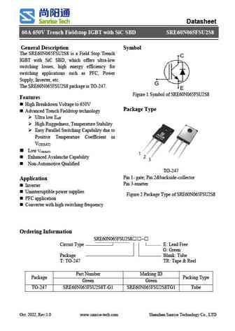
Datasheet 60A 650V Trench Fieldstop IGBT with SiC SBD SRE60N065FSU2S8 General Description Symbol The SRE60N065FSU2S8 is a Field Stop Trench IGBT with SiC SBD, which offers ultra-low switching losses, high energy efficiency for switching applications such as PFC, Power Supply, Inverter, etc. The SRE60N065FSU2S8 package is TO-247. Figure 1 Symbol of SRE60N065FSU2S8 Features
sre60n065fsudg.pdf
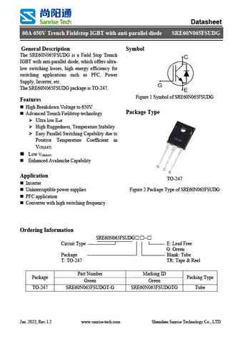
Datasheet 60A 650V Trench Fieldstop IGBT with anti-parallel diode SRE60N065FSUDG General Description Symbol The SRE60N065FSUDG is a Field Stop Trench IGBT with anti-parallel diode, which offers ultra- low switching losses, high energy efficiency for switching applications such as PFC, Power Supply, Inverter, etc. The SRE60N065FSUDG package is TO-247. Figure 1 Symbol of SRE60N06
sre160n065fsud8.pdf
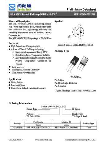
Preliminary Datasheet 160A 650V Trench Fieldstop IGBT with FRD SRE160N065FSUD8 General Description Symbol The SRE160N065FSUD8 is a Field Stop Trench IGBT with anti-parallel diode, which offers ultra low conduction loss, high energy efficiency for switching applications such as Inverter, Driver, Converter, etc. The SRE160N065FSUD8 package is TO-247Plus. Features Figure 1 Sy
sre60n065fsu.pdf
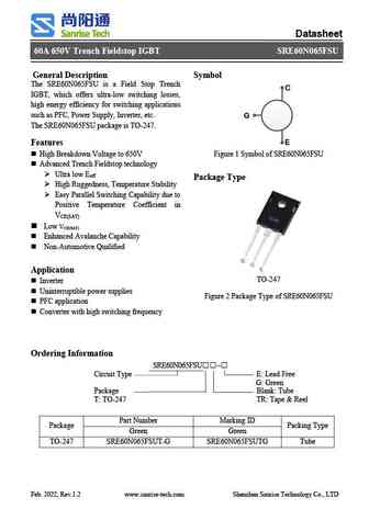
Datasheet 60A 650V Trench Fieldstop IGBT SRE60N065FSU General Description Symbol The SRE60N065FSU is a Field Stop Trench C IGBT, which offers ultra-low switching losses, high energy efficiency for switching applications such as PFC, Power Supply, Inverter, etc. G The SRE60N065FSU package is TO-247. E Features High Breakdown Voltage to 650V Figure 1 Symbol of SRE60N065
sl60n06.pdf
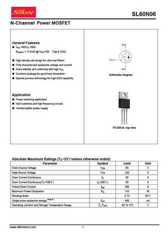
SL60N06 N-Channel Power MOSFET General Features VDS =60V,ID =60A RDS(ON)
cs60n06c4.pdf
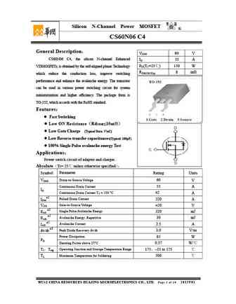
Silicon N-Channel Power MOSFET R CS60N06 C4 General Description VDSS 60 V CS60N06 C4, the silicon N-channel Enhanced ID 55 A PD(TC=25 ) 150 W VDMOSFETs, is obtained by the self-aligned planar Technology RDS(ON)Typ 8 m which reduce the conduction loss, improve switching performance and enhance the avalanche energy. The transistor can be used in various power
jmtg060n06a.pdf
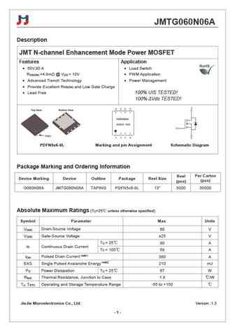
JMTG060N06A Description JMT N-channel Enhancement Mode Power MOSFET Features Application 60V,90 A Load Switch R
jmtc060n06a.pdf
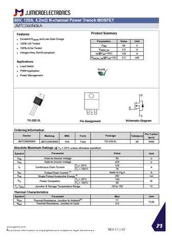
60V, 120A, 4.2m N-channel Power Trench MOSFET JMTC060N06A Product Summary Features Excellent RDS(ON) and Low Gate Charge Parameters Value Unit 100% UIS Tested VDSS 60 V 100% Vds Tested VGS(th)_Typ 3.0 V Halogen-free; RoHS-compliant ID(@VGS=10V) 120 A RDS(ON)_Typ(@VGS=10V 4.2 mW Applications Load Switch PWM Application Power Management D G S
jmtk060n06a.pdf
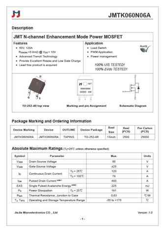
JMTK060N06A Description JMT N-channel Enhancement Mode Power MOSFET Features Application 60V, 120A Load Switch R
jmte060n06a.pdf
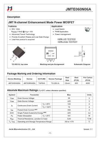
JMTE060N06A Description JMT N-channel Enhancement Mode Power MOSFET Features Application 60V, 120A Load Switch R
hgs060n06sl.pdf
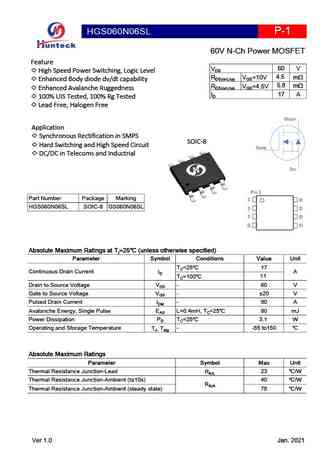
HGS060N06SL P-1 60V N-Ch Power MOSFET Feature 60 V VDS High Speed Power Switching, Logic Level 4.5 RDS(on),typ VGS=10V mW Enhanced Body diode dv/dt capability 5.8 RDS(on),typ VGS=4.5V mW Enhanced Avalanche Ruggedness 17 A ID 100% UIS Tested, 100% Rg Tested Lead Free, Halogen Free Drain Application Synchronous Rectification in SMPS SOIC-8 Hard Swit
wsf60n06.pdf
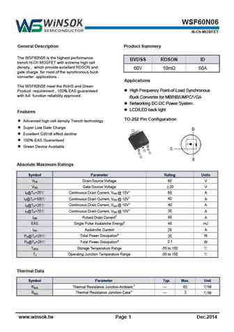
WSF60N06 N-Ch MOSFET General Description Product Summery The WSF60N06 is the highest performance BVDSS RDSON ID trench N-Ch MOSFET with extreme high cell density , which provide excellent RDSON and 60V 10m 60A gate charge for most of the synchronous buck converter applications . Applications The WSF60N06 meet the RoHS and Green High Frequency Point-of-Load Synchronous
wsr60n06.pdf
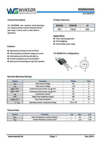
WSR60N06 N-Ch MOSFET General Description Product Summery The WSR60N06 uses advanced trench technology BVDSS RDSON ID and design to provide excellent R with low DS(ON) 60V 12m 60A gate charge. It can be used in a wide variety of applications. Application Power switching application LED backlighting Uninterruptible power supply Features High density cell
mtp60n06hd.pdf
MTP60N06HD www.VBsemi.tw N-Channel 60-V (D-S) MOSFET FEATURES PRODUCT SUMMARY 175 C Junction Temperature VDS (V) RDS(on) ( ) ID (A)a TrenchFET Power MOSFET 0.011 at VGS = 10 V 60 Material categorization 60 0.012 at VGS = 4.5 V 50 D TO-220AB G S D S G N-Channel MOSFET ABSOLUTE MAXIMUM RATINGS (TC = 25 C, unless otherwise noted) Parameter Symbol Lim
ntb60n06g.pdf

NTB60N06G www.VBsemi.tw N-Channel 60-V (D-S) MOSFET FEATURES PRODUCT SUMMARY 175 C Junction Temperature VDS (V) RDS(on) ( ) ID (A)a TrenchFET Power MOSFET 0.012 at VGS = 10 V 60 60 0.013 at VGS = 4.5 V 50 D D2PAK (TO-263) G G D S S N-Channel MOSFET ABSOLUTE MAXIMUM RATINGS (TC = 25 C, unless otherwise noted) Parameter Symbol Limit Unit VGS Gate-Sourc
vbzm60n06.pdf
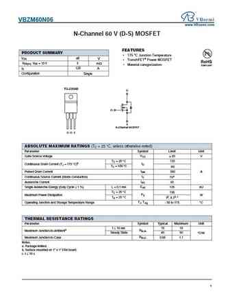
VBZM60N06 www.VBsemi.com N-Channel 60 V (D-S) MOSFET FEATURES PRODUCT SUMMARY 175 C Junction Temperature VDS 60 V TrenchFET Power MOSFET RDS(on) VGS = 10 V 5 m Material categorization ID 120 A Configuration Single TO-220AB D G S N-Channel MOSFET G D S ABSOLUTE MAXIMUM RATINGS (TC = 25 C, unless otherwise noted) Parameter Symbol Limit Unit VGS Gate-So
vbzl60n06.pdf
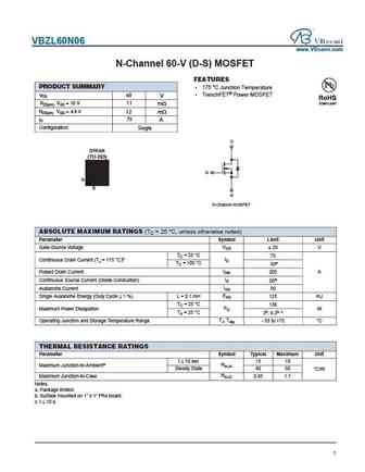
VBZL60N06 www.VBsemi.com N-Channel 60-V (D-S) MOSFET FEATURES PRODUCT SUMMARY 175 C Junction Temperature TrenchFET Power MOSFET VDS 60 V RDS(on) VGS = 10 V 11 m RDS(on) VGS = 4.5 V 12 m 75 ID A Configuration Single D D2PAK (TO-263) G G D S S N-Channel MOSFET ABSOLUTE MAXIMUM RATINGS (TC = 25 C, unless otherwise noted) Parameter Symbol Limit Unit V
ntp60n06.pdf
NTP60N06 www.VBsemi.tw N-Channel 60-V (D-S) MOSFET FEATURES PRODUCT SUMMARY 175 C Junction Temperature VDS (V) RDS(on) ( ) ID (A)a TrenchFET Power MOSFET 0.011 at VGS = 10 V 60 Material categorization 60 0.012 at VGS = 4.5 V 50 D TO-220AB G S D S G N-Channel MOSFET ABSOLUTE MAXIMUM RATINGS (TC = 25 C, unless otherwise noted) Parameter Symbol Limit
emb60n06a.pdf
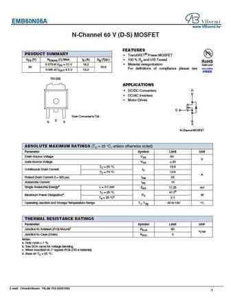
EMB60N06A www.VBsemi.tw N-Channel 60 V (D-S) MOSFET FEATURES PRODUCT SUMMARY TrenchFET Power MOSFET VDS (V) RDS(on) ( ) Max. ID (A) Qg (Typ.) 100 % Rg and UIS Tested 0.073 at VGS = 10 V 18.2 Material categorization 60 19.8 For definitions of compliance please see 0.085 at VGS = 4.5 V 13.2 TO-252 APPLICATIONS D DC/DC Converters DC/AC Inverters
stb60n06-14.pdf
STB60N06-14 www.VBsemi.tw N-Channel 60-V (D-S) MOSFET FEATURES PRODUCT SUMMARY 175 C Junction Temperature VDS (V) RDS(on) ( ) ID (A)a TrenchFET Power MOSFET 0.012 at VGS = 10 V 60 60 0.013 at VGS = 4.5 V 50 D D2PAK (TO-263) G G D S S N-Channel MOSFET ABSOLUTE MAXIMUM RATINGS (TC = 25 C, unless otherwise noted) Parameter Symbol Limit Unit VGS Gate-Sou
s60n06m.pdf
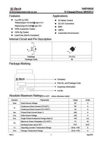
S60N06M SI-TECH SEMICONDUCTOR CO.,LTD N-Channel Power MOSFET Features Applications V =60V,I =60A DS D DC Motor Control Rds(on)(typ)=10.5m @Vgs=4.5V DC-DC Converters Rds(on)(typ)=8.5m @Vgs=10V BMS 100% Avalanche Tested SMPS 100% Rg Tested Automotive Environment Lead-Free (RoHS Compliant) Internal Circuit and Pin Descript
hm60n06k.pdf
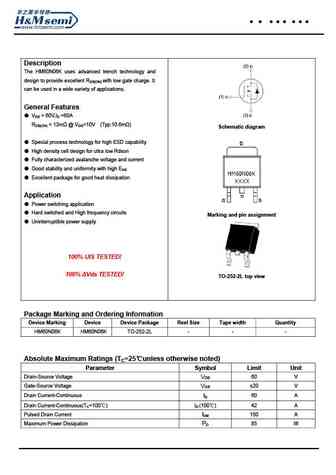
HM60N06K Description The HM60N06K uses advanced trench technology and design to provide excellent RDS(ON) with low gate charge. It can be used in a wide variety of applications. General Features VDS = 60V,ID =60A RDS(ON)
hm60n06.pdf
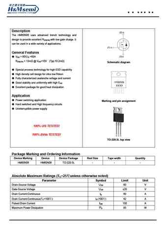
HM60N06 Description The HM60N06 uses advanced trench technology and design to provide excellent RDS(ON) with low gate charge. It can be used in a wide variety of applications. General Features VDS = 60V,ID =60A RDS(ON)
hms60n06d.pdf
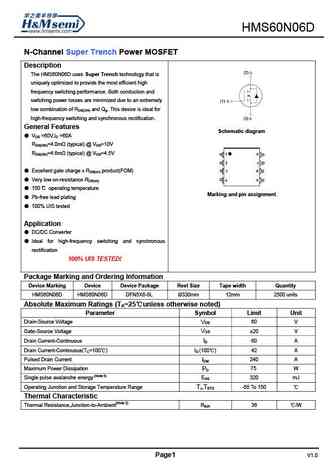
HMS60N06D N-Channel Super Trench Power MOSFET Description The HMS60N06D uses Super Trench technology that is uniquely optimized to provide the most efficient high frequency switching performance. Both conduction and switching power losses are minimized due to an extremely low combination of R and Q . This device is ideal for DS(ON) g high-frequency switching and synchronous re
mdt60n06d.pdf
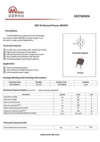
60V N-Channel Power MOSFE Description The MDT60N06 uses advanced trench technology to provide excellent RDS(ON), low gate charge. It can be used in a wide variety of applications. General Features V =60V, R
hpd160n06sta.pdf
HAOHAI ELECTRONICS HPD160N06STA Product Summary 50A, 60V VDS 60 V N-CHANNEL POWER MOSFET RDS(ON) Max. 16 m Features Advanced process technology ID 50 A Ultra low On-Resistance 150 Operating Temperature Fast Switching 2.Drain Repetitive Avalanche Allowed up to Tjmax Lead-Free D Mechanical Data Case TO-252 Case Material Molded Plastic Green Molding 1.
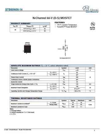
stp60n06-14.pdf
INCHANGE Semiconductor Isc N-Channel MOSFET Transistor STP60N06-14 FEATURES With low gate drive requirements Easy to drive High current capability 100% avalanche tested Minimum Lot-to-Lot variations for robust device performance and reliable operation APPLICATIONS Solenold and relay dirvers DC-DC converters Automotive environment ABSOLUTE MAXIMUM RATINGS(T =25
ipa060n06n.pdf
INCHANGE Semiconductor Isc N-Channel MOSFET Transistor IPA060N06N FEATURES With TO-220F package Low input capacitance and gate charge Low gate input resistance Reduced switching and conduction losses 100% avalanche tested Minimum Lot-to-Lot variations for robust device performance and reliable operation APPLICATIONS Switching applications ABSOLUTE MAXIMUM RATINGS
ipp060n06n.pdf
INCHANGE Semiconductor isc N-Channel MOSFET Transistor IPP060N06N IIPP060N06N FEATURES Static drain-source on-resistance RDS(on) 6.0m Enhancement mode Fast Switching Speed 100% avalanche tested Minimum Lot-to-Lot variations for robust device performance and reliable operation DESCRITION reliable device for use in a wide variety of applications ABSOLUTE M
60n06-14.pdf

isc N-Channel MOSFET Transistor 60N06-14 DESCRIPTION High current capability Avalanche rugged technology Low gate charge Fast Switching Speed Minimum Lot-to-Lot variations for robust device performance and reliable operation APPLICATIONS Regulator High current,high speed switching Solenoid and relay drivers ABSOLUTE MAXIMUM RATINGS(T =25 ) C SYMBOL ARAMETER V
ap60n06f.pdf
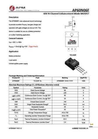
AP60N06F 60V N-Channel Enhancement Mode MOSFET Description The AP60N06F uses advanced trench technology to provide excellent R , low gate charge and DS(ON) operation with gate voltages as low as 4.5V. This device is suitable for use as a Battery protection or in other Switching application. General Features V = 60V I =60A DS D R
Другие IGBT... 12N10, 15N20, 19N10, 22N20, 25N06, 25N10, 30N06, 50N06, IRF520, 60N08, 6N10, 70N06, 75N75, 7N10, 7N10Z, 80N08, UF1010A
Параметры MOSFET. Взаимосвязь и компромиссы
🌐 : EN ES РУ

Список транзисторов
Обновления
MOSFET: BC3134KT | BC3134K | BC2302W | BC2302T-2.8A | BC2302-2.8A | BC2301W | BC2301T-2.8A | CB3139KTB | CB2301DW | BC8205 | BC3415 | BC3407 | BC3401 | BC3400 | BC2301 | BC1012W
Popular searches
d209l | irfb4321 | 2n333 | c3852 | irfp140 | ksc2383 datasheet | 2n3906 equivalent | a733 transistor equivalent