70N06 datasheet, аналоги, основные параметры
Наименование производителя: 70N06 📄📄
Тип транзистора: MOSFET
Полярность: N
Предельные значения
Pd ⓘ - Максимальная рассеиваемая мощность: 200 W
|Vds|ⓘ - Максимально допустимое напряжение сток-исток: 60 V
|Vgs|ⓘ - Максимально допустимое напряжение затвор-исток: 20 V
|Id| ⓘ - Максимально допустимый постоянный ток стока: 70 A
Tj ⓘ - Максимальная температура канала: 150 °C
Электрические характеристики
tr ⓘ - Время нарастания: 79 ns
Cossⓘ - Выходная емкость: 530 pf
RDSonⓘ - Сопротивление сток-исток открытого транзистора: 0.012 Ohm
Тип корпуса: TO-220
TO-263
TO-262
📄📄 Копировать
Аналог (замена) для 70N06
- подборⓘ MOSFET транзистора по параметрам
70N06 даташит
..1. Size:339K utc
70n06.pdf 
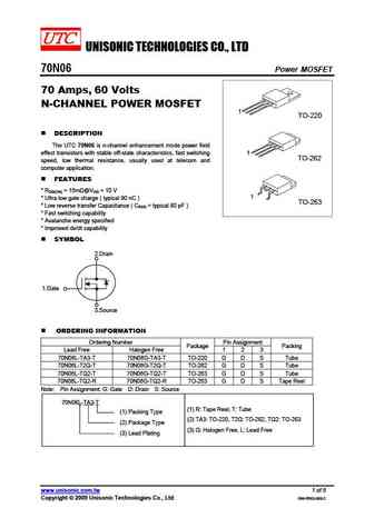
UNISONIC TECHNOLOGIES CO., LTD 70N06 Power MOSFET 70 Amps, 60 Volts N-CHANNEL POWER MOSFET 1 TO-220 DESCRIPTION The UTC 70N06 is n-channel enhancement mode power field effect transistors with stable off-state characteristics, fast switching 1 TO-262 speed, low thermal resistance, usually used at telecom and computer application. FEATURES * RDS(ON) = 15m @VGS = 10 V
..2. Size:231K inchange semiconductor
70n06.pdf 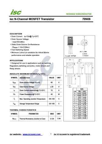
INCHANGE Semiconductor isc N-Channel MOSFET Transistor 70N06 DESCRIPTION Drain Current I =70A@ T =25 D C Drain Source Voltage- V =60V(Min) DSS Static Drain-Source On-Resistance R = 14m (Max) DS(on) Fast Switching Speed Minimum Lot-to-Lot variations for robust device performance and reliable operation APPLICATIONS Designed for use in applications such as swithi
..3. Size:236K inchange semiconductor
70n06 .pdf 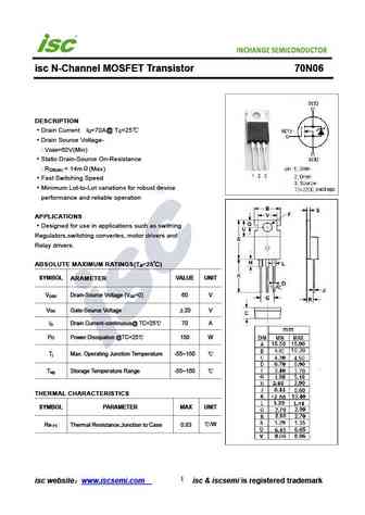
INCHANGE Semiconductor isc N-Channel MOSFET Transistor 70N06 DESCRIPTION Drain Current I =70A@ T =25 D C Drain Source Voltage- V =60V(Min) DSS Static Drain-Source On-Resistance R = 14m (Max) DS(on) Fast Switching Speed Minimum Lot-to-Lot variations for robust device performance and reliable operation APPLICATIONS Designed for use in applications such as swithi
0.1. Size:743K 1
ltp70n06p.pdf 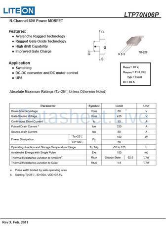
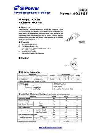
LTP70N06P N-Channel 60V Power MOSFET Features Avalanche Rugged Technology Rugged Gate Oxide Technology High di/dt Capability Improved Gate Charge Application BVDSS = 60 V, Switching RDS(ON ) = 11.5 m , DC-DC converter and DC motor control Typ = 9 m UPS ID = 80 A Absolute Maximum Ratings (TA=25 Unless Otherwise Noted) Parameter Symbol Limit Unit
0.2. Size:690K fairchild semi
fqa170n06.pdf 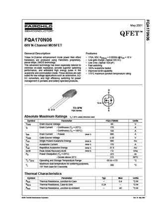
May 2001 TM QFET FQA170N06 60V N-Channel MOSFET General Description Features These N-Channel enhancement mode power field effect 170A, 60V, RDS(on) = 0.0056 @VGS = 10 V transistors are produced using Fairchild s proprietary, Low gate charge ( typical 220 nC) planar stripe, DMOS technology. Low Crss ( typical 620 pF) This advanced technology has been especially tailore
0.3. Size:229K fairchild semi
rfg70n06 rfp70n06 rf1s70n06 rf1s70n06sm.pdf 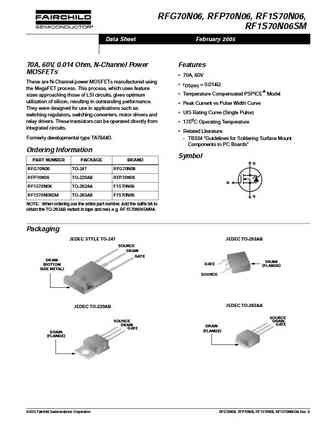
RFG70N06, RFP70N06, RF1S70N06, RF1S70N06SM Data Sheet February 2005 70A, 60V, 0.014 Ohm, N-Channel Power Features MOSFETs 70A, 60V These are N-Channel power MOSFETs manufactured using rDS(on) = 0.014 the MegaFET process. This process, which uses feature Temperature Compensated PSPICE Model sizes approaching those of LSI circuits, gives optimum utilization of silic
0.4. Size:227K fairchild semi
rf1s70n06.pdf 
RFG70N06, RFP70N06, RF1S70N06, RF1S70N06SM Data Sheet February 2005 70A, 60V, 0.014 Ohm, N-Channel Power Features MOSFETs 70A, 60V These are N-Channel power MOSFETs manufactured using rDS(on) = 0.014 the MegaFET process. This process, which uses feature Temperature Compensated PSPICE Model sizes approaching those of LSI circuits, gives optimum utilization of silic
0.5. Size:546K samsung
sfp70n06.pdf 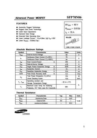
Advanced Power MOSFET FEATURES BVDSS = 60 V Avalanche Rugged Technology RDS(on) = 0.012 Rugged Gate Oxide Technology Lower Input Capacitance ID = 70 A Improved Gate Charge Extended Safe Operating Area TO-220 Lower Leakage Current 10 A (Max.) @ VDS = 60V Lower RDS(ON) 0.009 (Typ.) 1 2 3 1.Gate 2. Drain 3. Source Absolute Maximum Ratings Symbol Characteristic Value
0.6. Size:94K vishay
sup70n06-14 sub70n06-14.pdf 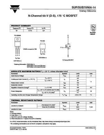
SUP/SUB70N06-14 Vishay Siliconix N-Channel 60-V (D-S), 175 C MOSFET PRODUCT SUMMARY V(BR)DSS (V) rDS(on) ( )ID (A) Pb-free 60 0.014 Available 70a RoHS* COMPLIANT TO-220AB D TO-263 G DRAIN connected to TAB G D S Top View G D S S SUB70N06-14 Top View N-Channel MOSFET SUP70N06-14 Ordering Information SUB70N06-14 SUB70N06-14-E3 (Lead (Pb)-free) SUP70N06-14-E3 (Lead (P
0.8. Size:894K infineon
ipb070n06ng ipp070n06ng ipi070n06ngrev1.4.pdf 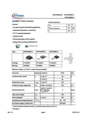
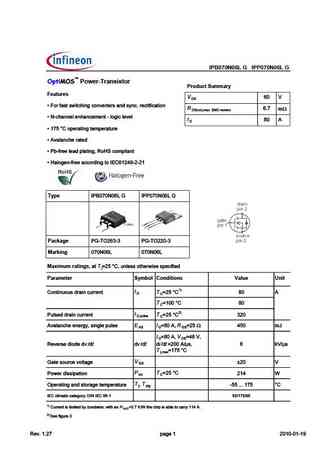
IPB070N06N G IPP070N06N G IPI070N06N G Power-Transistor Product Summary Features V D P &?F 71C5 381A75 6?A 61BC BF9C389>7 1@@B R 7 m , ?> =1G ,' E5AB9?> P ( 381>>581>35=5>C >?A=1
0.9. Size:693K onsemi
rfp70n06.pdf 
Is Now Part of To learn more about ON Semiconductor, please visit our website at www.onsemi.com Please note As part of the Fairchild Semiconductor integration, some of the Fairchild orderable part numbers will need to change in order to meet ON Semiconductor s system requirements. Since the ON Semiconductor product management systems do not have the ability to manage part nomenclatur
0.10. Size:2180K onsemi
fqa170n06.pdf 
Is Now Part of To learn more about ON Semiconductor, please visit our website at www.onsemi.com Please note As part of the Fairchild Semiconductor integration, some of the Fairchild orderable part numbers will need to change in order to meet ON Semiconductor s system requirements. Since the ON Semiconductor product management systems do not have the ability to manage part nomenclatur
0.11. Size:418K onsemi
ndba170n06a.pdf 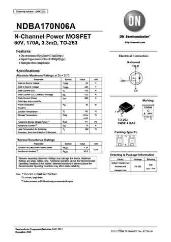
Ordering number ENA2250 NDBA170N06A N-Channel Power MOSFET http //onsemi.com 60V, 170A, 3.3m , TO-263 Features On-resistance RDS(on)=2.5m (typ.) Electrical Connection Input Capacitance Ciss=15800pF(typ.) N-channel Halogen free compliance D(2, 4) Specifications Absolute Maximum Ratings at Ta = 25 C Parameter Symbol Value Unit G(1) V Drain to Sourc
0.12. Size:86K intersil
rff70n06.pdf 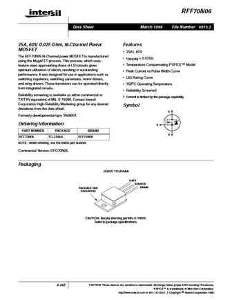
RFF70N06 Data Sheet March 1999 File Number 4073.2 25A, 60V, 0.025 Ohm, N-Channel Power Features MOSFET 25A , 60V The RFF70N06 N-Channel power MOSFET is manufactured rDS(ON) = 0.025 using the MegaFET process. This process, which uses Temperature Compensating PSPICE Model feature sizes approaching those of LSI circuits gives optimum utilization of silicon, resulting
0.13. Size:91K kec
kf70n06p f.pdf 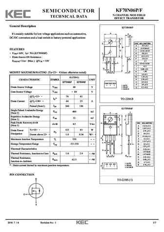
KF70N06P/F SEMICONDUCTOR N CHANNEL MOS FIELD TECHNICAL DATA EFFECT TRANSISTOR General Description KF70N06P A It s mainly suitable for low viltage applications such as automotive, O C DC/DC converters and a load switch in battery powered applications F E DIM MILLIMETERS G _ + A 9.9 0.2 B B 15.95 MAX FEATURES Q C 1.3+0.1/-0.05 _ VDSS= 60V, ID= 70A (KF70N06P) I + D 0
0.14. Size:858K blue-rocket-elect
br70n06.pdf 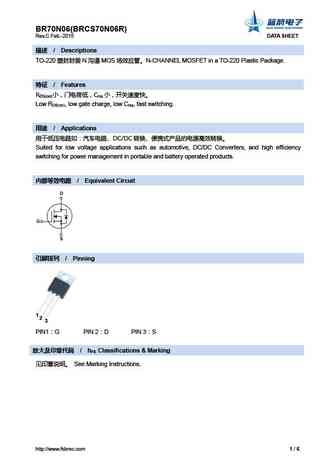
BR70N06(BRCS70N06R) Rev.C Feb.-2015 DATA SHEET / Descriptions TO-220 N MOS N-CHANNEL MOSFET in a TO-220 Plastic Package. / Features R C DS(on) rss Low RDS(on), low gate charge, low Crss, fast switching. / Applications DC/DC
0.15. Size:849K shantou-huashan
hfp70n06.pdf 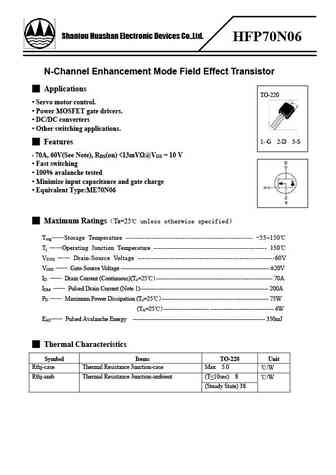
Shantou Huashan Electronic Devices Co.,Ltd. HFP70N06 N-Channel Enhancement Mode Field Effect Transistor Applications TO-220 Servo motor control. Power MOSFET gate drivers. DC/DC converters Other switching applications. 1- G 2-D 3-S Features 70A, 60V(See Note), RDS(on)
0.16. Size:570K first silicon
ftk70n06.pdf 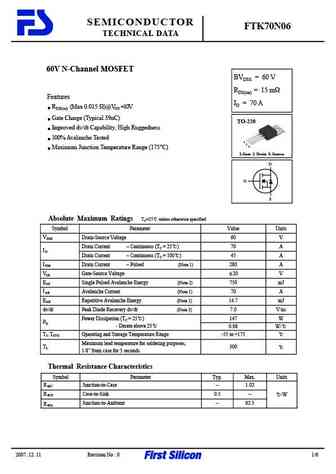
SEMICONDUCTOR FTK70N06 TECHNICAL DATA 60V N-Channel MOSFET BVDSS = 60 V RDS(on) = 15 m Features ID = 70 A RDS(on) (Max 0.015 )@VGS =10V Gate Charge (Typical 39nC) TO-220 Improved dv/dt Capability, High Ruggedness 100% Avalanche Tested 1 2 3 Maximum Junction Temperature Range (175 C) 1.Gate 2. Drain 3. Source D G S Absolute Maximum Ratings TC
0.17. Size:532K kexin
ndt70n06.pdf 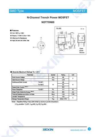
SMD Type MOSFET Transistors N-Channel Trench Power MOSFET NDT70N06 TO-252 Unit mm Features +0.15 6.50-0.15 +0.1 2.30 -0.1 VDS = 60V; ID = 88A +0.2 5.30-0.2 +0.8 0.50 -0.7 RDS(ON) 6.6m (VGS = 10V) Ultra Low On-Resistance High UIS and UIS 100% Test 0.127 +0.1 0.80-0.1 max + 0.1 1Gate 2.3 0.60- 0.1 +0.15 4.60 -0.15 2Drain 3Source Absolute Maximum Ratings Ta =
0.18. Size:508K winsemi
wfp70n06.pdf 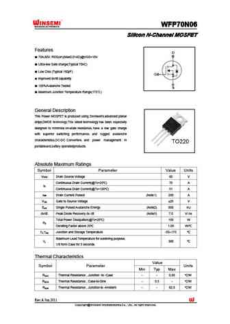
WFP70N06 WFP70N06 WFP70N06 WFP70N06 Silicon N-Channel MOSFET Silicon N-Channel MOSFET Silicon N-Channel MOSFET Silicon N-Channel MOSFET Features 70A,60V, RDS(on)(Max0.014 )@VGS=10V Ultra-low Gate charge(Typical 70nC) Low Crss (Typical 160pF) Improved dv/dt capability 100%Avalanche Tested Maximum Junction Temperature Range(175 ) General Description Thi
0.19. Size:565K winsemi
sfp70n06.pdf 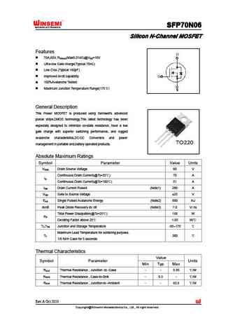
SFP70N06 SFP70N06 SFP70N06 SFP70N06 Silicon N-Channel MOSFET Silicon N-Channel MOSFET Silicon N-Channel MOSFET Silicon N-Channel MOSFET Features 70A,60V, R (Max0.014 )@V =10V DS(on) GS Ultra-low Gate charge(Typical 70nC) Low Crss (Typical 160pF) Improved dv/dt capability 100%Avalanche Tested Maximum Junction Temperature Range(175 ) General Description
0.20. Size:603K winsemi
wfp70n06t.pdf 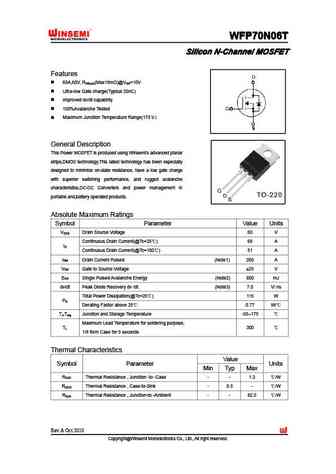
WFP70N06T WFP70N06T WFP70N06T WFP70N06T Silicon N-Channel MOSFET Silicon N-Channel MOSFET Silicon N-Channel MOSFET Silicon N-Channel MOSFET Features 68A,60V, R (Max18m )@V =10V DS(on) GS Ultra-low Gate charge(Typical 20nC) Improved dv/dt capability 100%Avalanche Tested Maximum Junction Temperature Range(175 ) General Description This Power MOSFET is produ
0.21. Size:590K liteon
ltp70n06.pdf 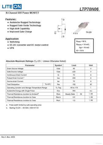
LTP70N06 N-Channel 60V Power MOSFET Features Avalanche Rugged Technology Rugged Gate Oxide Technology High di/dt Capability Improved Gate Charge Application BVDSS = 60 V, Switching RDS(ON ) = 14 m , DC-DC converter and DC motor control Typ = 10 m UPS ID = 70 A Absolute Maximum Ratings (TA=25 Unless Otherwise Noted) Parameter Symbol Limit Unit
0.22. Size:834K semihow
hrp70n06k.pdf 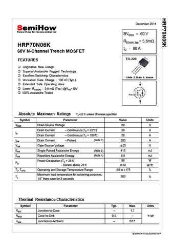
December 2014 BVDSS = 60 V RDS(on) typ = 5.6m HRP70N06K ID = 80 A 60V N-Channel Trench MOSFET TO-220 FEATURES Originative New Design Superior Avalanche Rugged Technology 1 2 3 Excellent Switching Characteristics 1.Gate 2. Drain 3. Source Unrivalled Gate Charge 100 nC (Typ.) Extended Safe Operating Area Lower RDS(ON) 5.6 m (Typ.)
0.23. Size:149K semihow
hrs70n06k.pdf 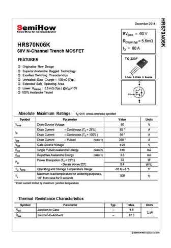
December 2014 BVDSS = 60 V RDS(on) typ HRS70N06K ID = 80 A 60V N-Channel Trench MOSFET TO-220F FEATURES Originative New Design Superior Avalanche Rugged Technology 1 2 3 Excellent Switching Characteristics 1.Gate 2. Drain 3. Source Unrivalled Gate Charge 100 nC (Typ.) Extended Safe Operating Area Lower RDS(ON) 5.6 (Typ.) @VGS=10V 100% Avalanche Test
0.26. Size:1267K jiejie micro
jmtp170n06d.pdf 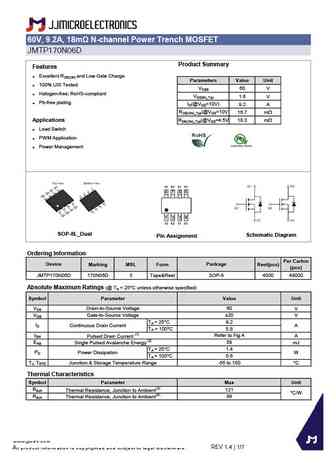
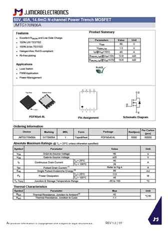
60V, 9.2A, 18m N-channel Power Trench MOSFET JMTP170N06D Product Summary Features Excellent RDS(ON) and Low Gate Charge Parameters Value Unit 100% UIS Tested VDSS 60 V Halogen-free; RoHS-compliant VGS(th)_Typ 1.6 V Pb-free plating ID(@VGS=10V) 9.2 A RDS(ON)_Typ(@VGS=10V 16.7 mW Applications RDS(ON)_Typ(@VGS=4.5V 18.3 mW Load Switch PWM Application
0.27. Size:419K jiejie micro
jmtg070n06a.pdf 
JMTG070N06A Description JMT N-channel Enhancement Mode Power MOSFET Features Application 60V, 70A Load Switch R
0.28. Size:339K jiejie micro
jmtp170n06a.pdf 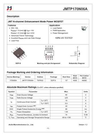
JMTP170N06A Description JMT N-channel Enhancement Mode Power MOSFET Features Application 60V, 10A Load Switch R
0.29. Size:816K cn vbsemi
70n06l-tq2.pdf 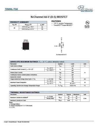
70N06L-TQ2 www.VBsemi.tw N-Channel 60-V (D-S) MOSFET FEATURES PRODUCT SUMMARY 175 C Junction Temperature VDS (V) RDS(on) ( ) ID (A)a TrenchFET Power MOSFET 0.012 at VGS = 10 V 60 60 0.013 at VGS = 4.5 V 50 D D2PAK (TO-263) G G D S S N-Channel MOSFET ABSOLUTE MAXIMUM RATINGS (TC = 25 C, unless otherwise noted) Parameter Symbol Limit Unit VGS Gate-Sour
0.30. Size:2304K cn si-tech
s70n06r s70n06s s70n06rn s70n06rp.pdf 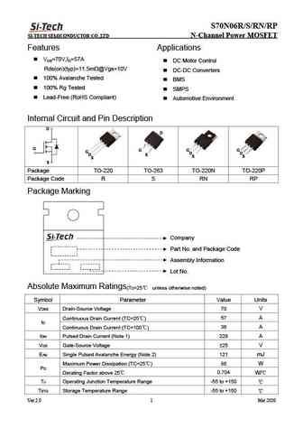
S70N06R/S/RN/RP SI-TECH SEMICONDUCTOR CO.,LTD N-Channel Power MOSFET Features Applications VDS=70V,ID=57A DC Motor Control Rds(on)(typ)=11.5m @Vgs=10V DC-DC Converters 100% Avalanche Tested BMS 100% Rg Tested SMPS Lead-Free (RoHS Compliant) Automotive Environment Internal Circuit and Pin Description D D G G G G G D D D
0.31. Size:230K inchange semiconductor
rfp70n06.pdf 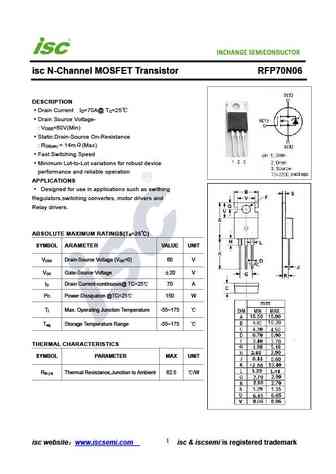
INCHANGE Semiconductor isc N-Channel MOSFET Transistor RFP70N06 DESCRIPTION Drain Current I =70A@ T =25 D C Drain Source Voltage- V =60V(Min) DSS Static Drain-Source On-Resistance R = 14m (Max) DS(on) Fast Switching Speed Minimum Lot-to-Lot variations for robust device performance and reliable operation APPLICATIONS Designed for use in applications such as sw
0.32. Size:211K inchange semiconductor
rfg70n06.pdf 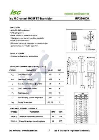
INCHANGE Semiconductor Isc N-Channel MOSFET Transistor RFG70N06 FEATURES With TO-247 packaging UIS rating curve Peak current vs pulse width curve High power and current handling capability 100% avalanche tested Minimum Lot-to-Lot variations for robust device performance and reliable operation APPLICATIONS High current switching applications ABSOLUTE MAXIMUM RATIN
0.33. Size:1534K cn apm
ap70n06hd.pdf 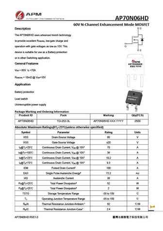
AP70N06HD 60V N-Channel Enhancement Mode MOSFET Description The AP70N06HD uses advanced trench technology to provide excellent R , low gate charge and DS(ON) operation with gate voltages as low as 10V. This device is suitable for use as a Battery protection or in other Switching application. General Features V = 60V I =70A DS D R
Другие IGBT... 22N20, 25N06, 25N10, 30N06, 50N06, 60N06, 60N08, 6N10, RU7088R, 75N75, 7N10, 7N10Z, 80N08, UF1010A, UF1010E, UF3710, UF4N20