7N10. Аналоги и основные параметры
Наименование производителя: 7N10
Тип транзистора: MOSFET
Полярность: N
Предельные значения
Pd ⓘ - Максимальная рассеиваемая мощность: 2.5 W
|Vds|ⓘ - Максимально допустимое напряжение сток-исток: 100 V
|Vgs|ⓘ - Максимально допустимое напряжение затвор-исток: 25 V
|Id| ⓘ - Максимально допустимый постоянный ток стока: 7 A
Tj ⓘ - Максимальная температура канала: 150 °C
Электрические характеристики
tr ⓘ - Время нарастания: 24 ns
Cossⓘ - Выходная емкость: 60 pf
RDSonⓘ - Сопротивление сток-исток открытого транзистора: 0.28 Ohm
Тип корпуса: TO-251 TO-252 SOT-223
Аналог (замена) для 7N10
- подборⓘ MOSFET транзистора по параметрам
7N10 даташит
7n10.pdf
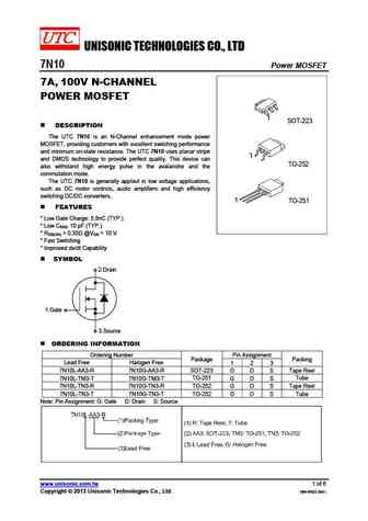
UNISONIC TECHNOLOGIES CO., LTD 7N10 Power MOSFET 7A, 100V N-CHANNEL POWER MOSFET 1 SOT-223 DESCRIPTION The UTC 7N10 is an N-Channel enhancement mode power MOSFET, providing customers with excellent switching performance and minimum on-state resistance. The UTC 7N10 uses planar stripe 1 and DMOS technology to provide perfect quality. This device can TO-252 also withstand
crst037n10n crss035n10n.pdf

CRST037N10N,CRSS035N10N ( ) SkyMOS1 N-MOSFET 100V, 3m , 120A Features Product Summary VDS Uses CRM(CQ) advanced SkyMOS1 technology 100V Extremely low on-resistance RDS(on) RDS(on) typ 3m Excellent QgxRDS(on) product(FOM) ID 120A Qualified according to JEDEC criteria Applications Motor control and drive 100% Avalanche Tested
ixth12n45ma ixth12n45mb ixth12n50ma ixth12n50mb ixth15n35ma ixth15n35mb ixth15n40ma ixth15n40mb ixtz42n20mb ixtz67n10ma ixtz67n10mb.pdf
mtp27n10erev0a.pdf

MOTOROLA Order this document SEMICONDUCTOR TECHNICAL DATA by MTP27N10E/D Designer's Data Sheet MTP27N10E TMOS E-FET. Motorola Preferred Device Power Field Effect Transistor N Channel Enhancement Mode Silicon Gate TMOS POWER FET This advanced TMOS power FET is designed to withstand high 27 AMPERES energy in the avalanche and commutation modes. This new energy 100 VOLTS e
mtp27n10e.pdf
MOTOROLA Order this document SEMICONDUCTOR TECHNICAL DATA by MTP27N10E/D Designer's Data Sheet MTP27N10E TMOS E-FET. Motorola Preferred Device Power Field Effect Transistor N Channel Enhancement Mode Silicon Gate TMOS POWER FET This advanced TMOS power FET is designed to withstand high 27 AMPERES energy in the avalanche and commutation modes. This new energy 100 VOLTS e
stl7n10f7.pdf
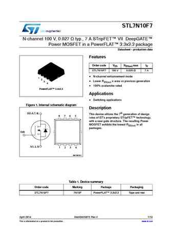
STL7N10F7 N-channel 100 V, 0.027 typ., 7 A STripFET VII DeepGATE Power MOSFET in a PowerFLAT 3.3x3.3 package Datasheet - production data Features Order code VDS RDS(on) max ID STL7N10F7 100 V 0.035 7 A N-channel enhancement mode 1 2 3 Lower RDS(on) x area vs previous generation 4 100% avalanche rated PowerFLAT 3.3x3.3 Applications Switching app
stf7n105k5.pdf
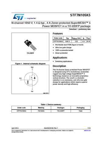
STF7N105K5 N-channel 1050 V, 1.4 typ., 4 A Zener-protected SuperMESH 5 Power MOSFET in a TO-220FP package Datasheet - preliminary data Features Order code VDS RDS(on) max. ID PTOT STF7N105K5 1050 V 2 4 A 25 W Worldwide best FOM (figure of merit) Ultra low gate charge 3 2 100% avalanche tested 1 Zener-protected TO-220FP Applications Switching applic
stp7n105k5 stu7n105k5 stw7n105k5.pdf
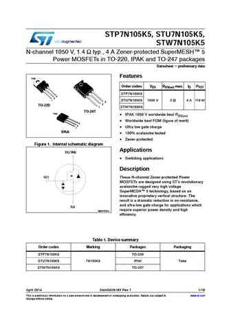
STP7N105K5, STU7N105K5, STW7N105K5 N-channel 1050 V, 1.4 typ., 4 A Zener-protected SuperMESH 5 Power MOSFETs in TO-220, IPAK and TO-247 packages Datasheet - preliminary data Features TAB Order codes VDS RDS(on) max. ID PTOT STP7N105K5 3 2 1 STU7N105K5 1050 V 2 4 A 110 W 3 2 TO-220 1 STW7N105K5 TO-247 TAB IPAK 1050 V worldwide best RDS(on) Worldwide best F
r07ds0209ej h7n1004fm.pdf
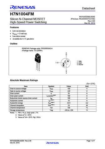
Preliminary Datasheet H7N1004FM R07DS0209EJ0200 (Previous REJ03G0073-0100) Silicon N-Channel MOSFET Rev.2.00 High-Speed Power Switching Dec 02, 2010 Features Low on-resistance RDS(on) = 25 m typ. Low drive current Available for 4.5 V gate drive Outline RENESAS Package code PRSS0003AD-A (Package name TO-220FM ) 2 D 1. Gate 1 G 2. Drain 3. Sou
rej03g1736 h7n1005dldsds.pdf

To our customers, Old Company Name in Catalogs and Other Documents On April 1st, 2010, NEC Electronics Corporation merged with Renesas Technology Corporation, and Renesas Electronics Corporation took over all the business of both companies. Therefore, although the old company name remains in this document, it is a valid Renesas Electronics document. We appreciate your understanding.
rej03g0391 h7n1005ldlslmds.pdf

To our customers, Old Company Name in Catalogs and Other Documents On April 1st, 2010, NEC Electronics Corporation merged with Renesas Technology Corporation, and Renesas Electronics Corporation took over all the business of both companies. Therefore, although the old company name remains in this document, it is a valid Renesas Electronics document. We appreciate your understanding.
rej03g1482 h7n1004dldsds.pdf
To our customers, Old Company Name in Catalogs and Other Documents On April 1st, 2010, NEC Electronics Corporation merged with Renesas Technology Corporation, and Renesas Electronics Corporation took over all the business of both companies. Therefore, although the old company name remains in this document, it is a valid Renesas Electronics document. We appreciate your understanding.
rej03g1131 h7n1002ldlslmds.pdf

To our customers, Old Company Name in Catalogs and Other Documents On April 1st, 2010, NEC Electronics Corporation merged with Renesas Technology Corporation, and Renesas Electronics Corporation took over all the business of both companies. Therefore, although the old company name remains in this document, it is a valid Renesas Electronics document. We appreciate your understanding.
h7n1002lm.pdf

To our customers, Old Company Name in Catalogs and Other Documents On April 1st, 2010, NEC Electronics Corporation merged with Renesas Technology Corporation, and Renesas Electronics Corporation took over all the business of both companies. Therefore, although the old company name remains in this document, it is a valid Renesas Electronics document. We appreciate your understanding.
rej03g0130 h7n1002ab.pdf

To our customers, Old Company Name in Catalogs and Other Documents On April 1st, 2010, NEC Electronics Corporation merged with Renesas Technology Corporation, and Renesas Electronics Corporation took over all the business of both companies. Therefore, although the old company name remains in this document, it is a valid Renesas Electronics document. We appreciate your understanding.
rej03g0072 h7n1004ldlslm.pdf

To our customers, Old Company Name in Catalogs and Other Documents On April 1st, 2010, NEC Electronics Corporation merged with Renesas Technology Corporation, and Renesas Electronics Corporation took over all the business of both companies. Therefore, although the old company name remains in this document, it is a valid Renesas Electronics document. We appreciate your understanding.
rej03g1579 h7n1004abds.pdf

To our customers, Old Company Name in Catalogs and Other Documents On April 1st, 2010, NEC Electronics Corporation merged with Renesas Technology Corporation, and Renesas Electronics Corporation took over all the business of both companies. Therefore, although the old company name remains in this document, it is a valid Renesas Electronics document. We appreciate your understanding.
fqd7n10ltf fqd7n10ltm fqd7n10l fqu7n10l fqu7n10ltu.pdf
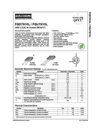
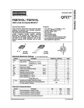
October 2008 QFET FQD7N10L / FQU7N10L 100V LOGIC N-Channel MOSFET General Description Features These N-Channel enhancement mode power field effect 5.8A, 100V, RDS(on) = 0.35 @VGS = 10 V transistors are produced using Fairchild s proprietary, Low gate charge ( typical 4.6 nC) planar stripe, DMOS technology. Low Crss ( typical 12 pF) This advanced technology is especia
fqpf7n10.pdf
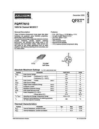
December 2000 TM QFET QFET QFET QFET FQPF7N10 100V N-Channel MOSFET General Description Features These N-Channel enhancement mode power field effect 5.5A, 100V, RDS(on) = 0.35 @VGS = 10 V transistors are produced using Fairchild s proprietary, Low gate charge ( typical 5.8 nC) planar stripe, DMOS technology. Low Crss ( typical 10 pF) This advanced technology is esp
fqp7n10.pdf
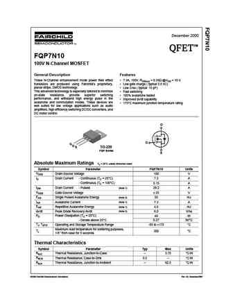
December 2000 TM QFET QFET QFET QFET FQP7N10 100V N-Channel MOSFET General Description Features These N-Channel enhancement mode power field effect 7.3A, 100V, RDS(on) = 0.35 @VGS = 10 V transistors are produced using Fairchild s proprietary, Low gate charge ( typical 5.8 nC) planar stripe, DMOS technology. Low Crss ( typical 10 pF) This advanced technology is espe
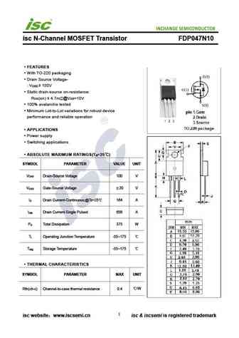
fdp047n10.pdf
August 2008 FDP047N10 tm N-Channel PowerTrench MOSFET 100V, 164A, 4.7m Description General Description RDS(on) = 3.9m ( Typ.) @ VGS = 10V, ID = 75A This N-Channel MOSFET is producedusing Fairchild Semicon- ductor s advance PowerTrench process that has been especially Fast switching speed tailored to minimize the on-state resistance and yet maintain superior switch
fqi7n10tu.pdf
December 2000 TM QFET QFET QFET QFET FQB7N10 / FQI7N10 100V N-Channel MOSFET General Description Features These N-Channel enhancement mode power field effect 7.3A, 100V, RDS(on) = 0.35 @VGS = 10 V transistors are produced using Fairchild s proprietary, Low gate charge ( typical 5.8 nC) planar stripe, DMOS technology. Low Crss ( typical 10 pF) This advanced technolo
fqt7n10tf.pdf
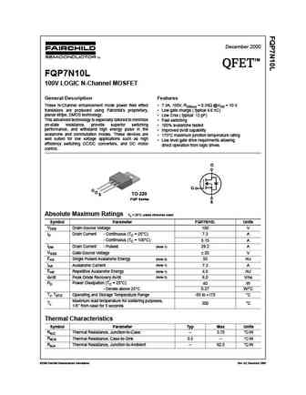
May 2001 TM QFET FQT7N10 100V N-Channel MOSFET General Description Features These N-Channel enhancement mode power field effect 1.7A, 100V, RDS(on) = 0.35 @VGS = 10 V transistors are produced using Fairchild s proprietary, Low gate charge ( typical 5.8 nC) planar stripe, DMOS technology. Low Crss ( typical 10 pF) This advanced technology has been especially tailored t
fdb047n10.pdf
August 2008 FDB047N10 tm N-Channel PowerTrench MOSFET 100V, 164A, 4.7m Description General Description RDS(on) = 3.9m ( Typ.) @ VGS = 10V, ID = 75A This N-Channel MOSFET is producedusing Fairchild Semicon- ductor s advance PowerTrench process that has been especially Fast switching speed tailored to minimize the on-state resistance and yet maintain superior switch
fqp7n10l.pdf
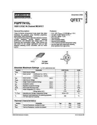
December 2000 TM QFET QFET QFET QFET FQP7N10L 100V LOGIC N-Channel MOSFET General Description Features These N-Channel enhancement mode power field effect 7.3A, 100V, RDS(on) = 0.35 @VGS = 10 V transistors are produced using Fairchild s proprietary, Low gate charge ( typical 4.6 nC) planar stripe, DMOS technology. Low Crss ( typical 12 pF) This advanced technology
fqt7n10ltf.pdf
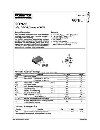
May 2001 TM QFET FQT7N10L 100V LOGIC N-Channel MOSFET General Description Features These N-Channel enhancement mode power field effect 1.7A, 100V, RDS(on) = 0.35 @VGS = 10 V transistors are produced using Fairchild s proprietary, Low gate charge ( typical 4.6 nC) planar stripe, DMOS technology. Low Crss ( typical 12 pF) This advanced technology has been especially tai
fqt7n10l.pdf

May 2001 TM QFET FQT7N10L 100V LOGIC N-Channel MOSFET General Description Features These N-Channel enhancement mode power field effect 1.7A, 100V, RDS(on) = 0.35 @VGS = 10 V transistors are produced using Fairchild s proprietary, Low gate charge ( typical 4.6 nC) planar stripe, DMOS technology. Low Crss ( typical 12 pF) This advanced technology has been especially tai
fqpf7n10l.pdf
December 2000 TM QFET QFET QFET QFET FQPF7N10L 100V LOGIC N-Channel MOSFET General Description Features These N-Channel enhancement mode power field effect 5.5A, 100V, RDS(on) = 0.35 @VGS = 10 V transistors are produced using Fairchild s proprietary, Low gate charge ( typical 4.6 nC) planar stripe, DMOS technology. Low Crss ( typical 12 pF) This advanced technology
fqt7n10.pdf

May 2001 TM QFET FQT7N10 100V N-Channel MOSFET General Description Features These N-Channel enhancement mode power field effect 1.7A, 100V, RDS(on) = 0.35 @VGS = 10 V transistors are produced using Fairchild s proprietary, Low gate charge ( typical 5.8 nC) planar stripe, DMOS technology. Low Crss ( typical 10 pF) This advanced technology has been especially tailored t
fqd7n10tm.pdf
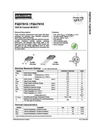
October 2008 QFET FQD7N10 / FQU7N10 100V N-Channel MOSFET General Description Features These N-Channel enhancement mode power field effect 5.8A, 100V, RDS(on) = 0.35 @VGS = 10 V transistors are produced using Fairchild s proprietary, Low gate charge ( typical 5.8 nC) planar stripe, DMOS technology. Low Crss ( typical 10 pF) This advanced technology is especially tail
fqb7n10ltm fqi7n10ltu.pdf
December 2000 TM QFET QFET QFET QFET FQB7N10L / FQI7N10L 100V LOGIC N-Channel MOSFET General Description Features These N-Channel enhancement mode power field effect 7.3A, 100V, RDS(on) = 0.35 @VGS = 10 V transistors are produced using Fairchild s proprietary, Low gate charge ( typical 4.6 nC) planar stripe, DMOS technology. Low Crss ( typical 12 pF) This advanced
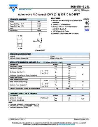
sum47n10-24l.pdf

SUM47N10-24L Vishay Siliconix N-Channel 100-V (D-S) 175 C MOSFET FEATURES PRODUCT SUMMARY TrenchFET Power MOSFET VDS (V) rDS(on) ( )ID (A) 175 C Maximum Junction Temperature RoHS 0.024 at VGS = 10 V 47 100 COMPLIANT 100 % Rg Tested 0.027 at VGS = 4.5 V 44 D TO-263 G G D S Top View S Ordering Information SUM47N10-24L-E3 (Lead (Pb)-free) N-Channel M
sum47n10.pdf
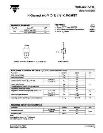
SUM47N10-24L Vishay Siliconix N-Channel 100-V (D-S) 175 C MOSFET FEATURES PRODUCT SUMMARY TrenchFET Power MOSFET VDS (V) rDS(on) ( )ID (A) 175 C Maximum Junction Temperature RoHS 0.024 at VGS = 10 V 47 100 COMPLIANT 100 % Rg Tested 0.027 at VGS = 4.5 V 44 D TO-263 G G D S Top View S Ordering Information SUM47N10-24L-E3 (Lead (Pb)-free) N-Channel M
bsz097n10ns5.pdf
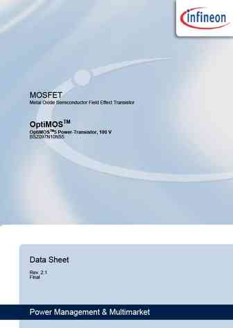
MOSFET Metal Oxide Semiconductor Field Effect Transistor OptiMOSTM OptiMOSTM5 Power-Transistor, 100 V BSZ097N10NS5 Data Sheet Rev. 2.1 Final Power Management & Multimarket OptiMOSTM5 Power-Transistor, 100 V BSZ097N10NS5 TSDSON-8 FL 1 Description (enlarged source interconnection) Features Ideal for high frequency switching Optimized technology for DC/DC converters E
ipi47n10s-33 ipp47n10s-33 ipb47n10s-33.pdf
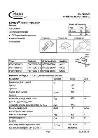
IPI47N10S-33 IPP47N10S-33, IPB47N10S-33 SIPMOS =Power-Transistor = == Product Summary Feature VDS 100 V N-Channel RDS(on) 33 m Enhancement mode ID 47 A 175 C operating temperature P-TO262-3-1 P-TO263-3-2 P-TO220-3-1 Avalanche rated dv/dt rated Type Package Ordering Code Marking IPP47N10S-33 PG-TO220-3-1 SP0002-25706 N1033 IPB47N10S-33 PG-TO263-3-2 SP00
ipb47n10sl-26 ipp47n10sl-26 ipi47n10sl-26.pdf
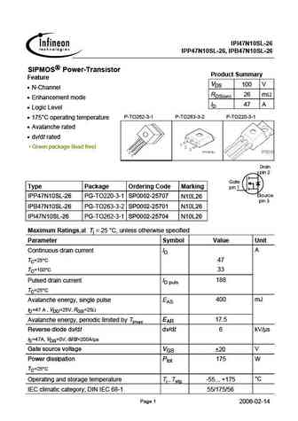
IPI47N10SL-26 IPP47N10SL-26, IPB47N10SL-26 SIPMOS =Power-Transistor = == Product Summary Feature VDS 100 V N-Channel RDS(on) 26 m Enhancement mode ID 47 A Logic Level P-TO262-3-1 P-TO263-3-2 P-TO220-3-1 175 C operating temperature Avalanche rated dv/dt rated Green package (lead free) Type Package Ordering Code Marking IPP47N10SL-26 PG-TO220-3-1 S
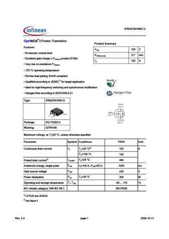
ipb027n10n5.pdf

MOSFET Metal Oxide Semiconductor Field Effect Transistor OptiMOSTM OptiMOS 5 Power-Transistor, 100 V IPB027N10N5 Data Sheet Rev. 2.1 Final Power Management & Multimarket OptiMOS 5 Power-Transistor, 100 V IPB027N10N5 D PAK 1 Description Features Ideal for high frequency switching and sync. rec. Excellent gate charge x R product (FOM) DS(on) Very low on-resista
ipb027n10n3g.pdf
IPB027N10N3 G 3 Power-Transistor Product Summary Features V 1 D Q ' 381>>5?B=1
ipb017n10n5.pdf

MOSFET Metal Oxide Semiconductor Field Effect Transistor OptiMOSTM OptiMOS 5 Power-Transistor, 100 V IPB017N10N5 Data Sheet Rev. 2.1 Final Power Management & Multimarket OptiMOS 5 Power-Transistor, 100 V IPB017N10N5 D -PAK 7pin 1 Description Features Ideal for high frequency switching and sync. rec. tab Excellent gate charge x R product (FOM) DS(on) Very low
bsc027n10ns5.pdf
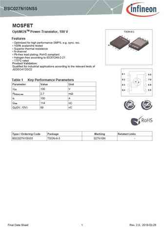
BSC027N10NS5 MOSFET TSON-8-3 OptiMOSTM Power-Transistor, 100 V 8 7 5 6 6 Features 7 5 8 Optimized for high performance SMPS, e.g. sync. rec. Pin 1 100% avalanche tested 2 4 3 3 Superior thermal resistance 4 2 1 N-channel Pb-free lead plating; RoHS compliant Halogen-free according to IEC61249-2-21 175 C rated Product Validation Qualified fo
spb47n10.pdf
Preliminary Data SPP 47N10 SIPMOS Power Transistor Product Summary Features Drain source voltage 100 V VDS N channel Drain-Source on-state resistance 0.033 RDS(on) Enhancement mode Continuous drain current 47 A ID Avalanche rated dv/dt rated 175 C operating temperature Pin 1 Pin 2 Pin 3 Type Package Ordering Code Packaging G D S SPP47N10 P-TO220-3-
ipb017n10n5lf.pdf
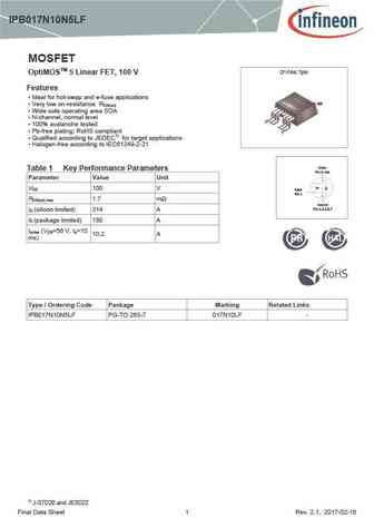
IPB017N10N5LF MOSFET D -PAK 7pin OptiMOSTM 5 Linear FET, 100 V Features Ideal for hot-swap and e-fuse applications tab Very low on-resistance R DS(on) Wide safe operating area SOA N-channel, normal level 1 100% avalanche tested Pb-free plating; RoHS compliant 7 Qualified according to JEDEC1) for target applications Halogen-free according to IEC61
ixgh17n100u1.pdf
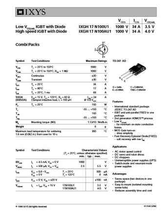
VCES IC25 VCE(sat) Low VCE(sat) IGBT with Diode IXGH 17 N100U1 1000 V 34 A 3.5 V High speed IGBT with Diode IXGH 17 N100AU1 1000 V 34 A 4.0 V Combi Packs Symbol Test Conditions Maximum Ratings TO-247 AD VCES TJ = 25 C to 150 C 1000 V VCGR TJ = 25 C to 150 C; RGE = 1 M 1000 V VGES Continuous 20 V G C VGEM Transient 30 V E IC25 TC = 25 C34 A G = Gate, C = Collector, IC90
ixth67n10 ixtm67n10 ixth75n10 ixtm75n10 ixtt75n10.pdf
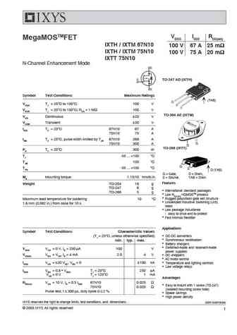
VDSS ID25 RDS(on) MegaMOSTMFET IXTH / IXTM 67N10 100 V 67 A 25 m IXTH / IXTM 75N10 100 V 75 A 20 m IXTT 75N10 N-Channel Enhancement Mode TO-247 AD (IXTH) Symbol Test Conditions Maximum Ratings (TAB) VDSS TJ = 25 C to 150 C 100 V VDGR TJ = 25 C to 150 C; RGS = 1 M 100 V TO-204 AE (IXTM) VGS Continuous 20 V VGSM Transient 30
ixfh7n100p.pdf
Polar TM HiPerFETTM VDSS = 1000V IXFA7N100P Power MOSFETs ID25 = 7A IXFP7N100P RDS(on) 1.9 IXFH7N100P N-Channel Enhancement Mode TO-263 AA (IXFA) Avalanche Rated Fast Intrinsic Rectifier G S D (Tab) TO-220AB (IXFP) Symbol Test Conditions Maximum Ratings VDSS TJ = 25 C to 150 C 1000 V VDGR TJ = 25 C to 150 C, RGS = 1M 1000 V VGSS Conti
ixgh17n100.pdf
VCES IC25 VCE(sat) Low VCE(sat) IGBT IXGH/IXGM 17 N100 1000 V 34 A 3.5 V High speed IGBT IXGH/IXGM 17 N100A 1000 V 34 A 4.0 V Symbol Test Conditions Maximum Ratings TO-247 AD (IXGH) VCES TJ = 25 C to 150 C 1000 V VCGR TJ = 25 C to 150 C; RGE = 1 M 1000 V VGES Continuous 20 V G C VGEM Transient 30 V E IC25 TC = 25 C34 A IC90 TC = 90 C17 A TO-204 AE (IXGM) ICM TC = 25 C
ixgh17n100au1.pdf

VCES IC25 VCE(sat) Low VCE(sat) IGBT with Diode IXGH 17 N100U1 1000 V 34 A 3.5 V High speed IGBT with Diode IXGH 17 N100AU1 1000 V 34 A 4.0 V Combi Packs Symbol Test Conditions Maximum Ratings TO-247 AD VCES TJ = 25 C to 150 C 1000 V VCGR TJ = 25 C to 150 C; RGE = 1 M 1000 V VGES Continuous 20 V G C VGEM Transient 30 V E IC25 TC = 25 C34 A G = Gate, C = Collector, IC90
ixgm17n100.pdf

VCES IC25 VCE(sat) Low VCE(sat) IGBT IXGH/IXGM 17 N100 1000 V 34 A 3.5 V High speed IGBT IXGH/IXGM 17 N100A 1000 V 34 A 4.0 V Symbol Test Conditions Maximum Ratings TO-247 AD (IXGH) VCES TJ = 25 C to 150 C 1000 V VCGR TJ = 25 C to 150 C; RGE = 1 M 1000 V VGES Continuous 20 V G C VGEM Transient 30 V E IC25 TC = 25 C34 A IC90 TC = 90 C17 A TO-204 AE (IXGM) ICM TC = 25 C
ixgm17n100a.pdf

VCES IC25 VCE(sat) Low VCE(sat) IGBT IXGH/IXGM 17 N100 1000 V 34 A 3.5 V High speed IGBT IXGH/IXGM 17 N100A 1000 V 34 A 4.0 V Symbol Test Conditions Maximum Ratings TO-247 AD (IXGH) VCES TJ = 25 C to 150 C 1000 V VCGR TJ = 25 C to 150 C; RGE = 1 M 1000 V VGES Continuous 20 V G C VGEM Transient 30 V E IC25 TC = 25 C34 A IC90 TC = 90 C17 A TO-204 AE (IXGM) ICM TC = 25 C
ixgh17n100a.pdf

VCES IC25 VCE(sat) Low VCE(sat) IGBT IXGH/IXGM 17 N100 1000 V 34 A 3.5 V High speed IGBT IXGH/IXGM 17 N100A 1000 V 34 A 4.0 V Symbol Test Conditions Maximum Ratings TO-247 AD (IXGH) VCES TJ = 25 C to 150 C 1000 V VCGR TJ = 25 C to 150 C; RGE = 1 M 1000 V VGES Continuous 20 V G C VGEM Transient 30 V E IC25 TC = 25 C34 A IC90 TC = 90 C17 A TO-204 AE (IXGM) ICM TC = 25 C
fdp047n10.pdf

Is Now Part of To learn more about ON Semiconductor, please visit our website at www.onsemi.com Please note As part of the Fairchild Semiconductor integration, some of the Fairchild orderable part numbers will need to change in order to meet ON Semiconductor s system requirements. Since the ON Semiconductor product management systems do not have the ability to manage part nomenclatur
fqt7n10l.pdf

Is Now Part of To learn more about ON Semiconductor, please visit our website at www.onsemi.com Please note As part of the Fairchild Semiconductor integration, some of the Fairchild orderable part numbers will need to change in order to meet ON Semiconductor s system requirements. Since the ON Semiconductor product management systems do not have the ability to manage part nomenclatur
fdb1d7n10cl7.pdf
FDB1D7N10CL7 N-Channel Shielded Gate POWERTRENCH) MOSFET 100 V, 268 A, 1.7 mW Description www.onsemi.com This N-Channel MOSFET is produced using ON Semiconductor s advanced POWERTRENCH process that incorporates Shielded Gate technology. This process has been optimized to minimize on-state VDS ID MAX rDS(on) MAX resistance and yet maintain superior switching performance with best in
7n10z.pdf
UNISONIC TECHNOLOGIES CO., LTD 7N10Z Power MOSFET 7A, 100V N-CHANNEL POWER MOSFET DESCRIPTION The UTC 7N10Z is an N-Channel enhancement mode power MOSFET providing customers with excellent switching performance and minimum on-state resistance. The UTC 7N10Z uses planar stripe and DMOS technology to provide perfect quality. This device can also withstand high energy pulse i
7n10l 7n10g.pdf
UNISONIC TECHNOLOGIES CO., LTD 7N10 Power MOSFET 7A, 100V N-CHANNEL POWER MOSFET DESCRIPTION The UTC 7N10 is an N-Channel enhancement mode power MOSFET, providing customers with excellent switching performance and minimum on-state resistance. The UTC 7N10 uses planar stripe and DMOS technology to provide perfect quality. This device can also withstand high energy pulse in the
rfd7n10le-sm rfp7n10le.pdf
RFD7N10LE, RFD7N10LESM S E M I C O N D U C T O R RFP7N10LE 7A, 100V, ESD Rated, Avalanche Rated, Logic Level N-Channel Enhancement-Mode Power MOSFETs (MegaFETs) February 1994 Features Packaging JEDEC TO-220AB 7A, 100V TOP VIEW rDS(ON) = 0.300 SOURCE 2KV ESD Protected DRAIN DRAIN (FLANGE) Temperature Compensating PSPICE Model GATE Can be Driven Directly fr
rfd7n10le-sm.pdf
RFD7N10LE, RFD7N10LESM Data Sheet October 1999 File Number 3598.3 7A, 100V, 0.300 Ohm, N-Channel, Logic Features Level, Power MOSFETs 7A, 100V These N-Channel power MOSFETs are manufactured using rDS(ON) = 0.300 a modern process. This process, which uses feature sizes Temperature Compensating PSPICE Model approaching those of LSI integrated circuits gives optimum util
cjq07n10.pdf
JIANGSU CHANGJING ELECTRONICS TECHNOLOGY CO., LTD SOP8 Plastic-Encapsulate MOSFETS CJQ07N10 N-Channel Power MOSFET DESCRIPTION SOP8 The device is the highest performance trench N-ch MOSFETs with extreme high cell density , which provide excellent R and gate charge for most of DSON the synchronous buck converter applications . 100% EAS guaranteed with full function reliability ap
msaer57n10a.pdf
2830 S. Fairview St. Santa Ana, CA 92704 PH (714) 979-8220 FAX (714) 966-5256 MSAER57N10A Features 100 Volts MOSKEYTM - Mosfet and Schottky in a single package 57 Amps Ultra Low On-Resistance 175 C Operating Temperature 25 m Increased Unclamped Inductive Switching (UIS) capability Hermetically sealed, surface mount power package N-CHANNEL
mtbc7n10n3.pdf
Spec. No. C886N3 Issued Date 2012.11.14 CYStech Electronics Corp. Revised Date Page No. 1/9 100V N-Channel Logic Level Enhancement Mode MOSFET BVDSS 100V MTBC7N10N3 ID 1A RDSON(TYP)@VGS=10V, ID=1A 389m RDSON(TYP)@VGS=4.5V, ID=1A 413m RDSON(TYP)@VGS=4V, ID=1A 407m Features Lower gate charge. ESD protected. Pb-free lead plating and Halogen-fre
brd17n10.pdf
BRD17N10(BRCS17N10D) Rev.C Feb.-2015 DATA SHEET / Descriptions TO-252 N MOS N-CHANNEL MOSFET in a TO-252 Plastic Package. / Features , Low gate charge, fast switching. / Applications DC/DC These devices are well suited for high efficiency switching DC/
hfp17n10.pdf
Shantou Huashan Electronic Devices Co.,Ltd. HFP17N10 N-Channel Enhancement Mode Field Effect Transistor General Description These are N-Channel enhancement mode silicon gate power field effect transistors. TO-220 They are advanced power MOSFETs designed, this advanced technology has been especially tailored to minimize on-state resistance, provide superior switching performanc
crst060n10n crss057n10n.pdf
CRST060N10N, CRSS057N10N ( ) SkyMOS1 N-MOSFET 100V, 5.3m , 120A Features Product Summary VDS Uses CRM(CQ) advanced SkyMOS1 technology 100V Extremely low on-resistance RDS(on) RDS(on) 5.3m Excellent QgxRDS(on) product(FOM) ID 120A Qualified according to JEDEC criteria Applications Motor control and drive 100% Avalanche Tested
crst040n10n crss037n10n.pdf
CRST040N10N, CRSS037N10N ( ) SkyMOS1 N-MOSFET 100V, 3.3m , 120A Features Product Summary VDS Uses CRM(CQ) advanced SkyMOS1 technology 100V Extremely low on-resistance RDS(on) RDS(on) 3.3m Excellent QgxRDS(on) product(FOM) ID 120A Qualified according to JEDEC criteria Applications Motor control and drive 100% Avalanche Tested
kx7n10l.pdf
SMDType MOSFET DIP Type MOSFET SMDType MOSFET DIP Type MOSFET SMD Type IC SMD Type IC Product specification KX7N10L SOT-223 Unit mm Features 3.50+0.2 6.50+0.2 -0.2 -0.2 VDS (V) = 100V ID = 1.7 A (VGS = 10V) 0.90+0.2 -0.2 350m (V = 10V), I =0.85A DS(ON) GS D +0.1 R 3.00-0.1 7.00+0.3 -0.3 380m (V = 5V), I =0.85A DS(ON) GS D R 4
ki7n10dy.pdf
SMD Type MOSFET N-Channel MOSFET KI7N10DY SOP-8 Features VDS (V) = 100V ID = 7A (VGS = 10V) 1.50 0.15 RDS(ON) 350m (VGS = 10V) 1 Source 5 Drain 6 Drain 2 Source 7 Drain 3 Source 8 Drain 4 Gate Absolute Maximum Ratings Ta = 25 Parameter Symbol Rating Unit Drain-Source Voltage VDS 100 V Gate-Source Voltage VGS 20 Continuous Drain Current I
wmb037n10hgs.pdf
WMB037N10HGS 100V N-Channel Enhancement Mode Power MOSFET Description D D D D D D D D WMB037N10HGS uses Wayon's advanced power trench MOSFET G ss technology that has been especially tailored to minimize the on-state s ss G s resistance and yet maintain superior switching performance. This device is well suited for high efficiency fast switching applications. PDFN5060-8
wml07n100c2 wmn07n100c2 wmm07n100c2 wmj07n100c2 wmo07n100c2 wmp07n100c2 wmk07n100c2.pdf

WM 2, WMN07N MM07N100C ML07N100C2 N100C2, WM C2 WMJ07N100C2, WM C2, WMP07N MK07N100C MO07N100C N100C2, WM C2 1000V Super Ju MOSFET V 2.0 S unction Power M T Descrip ption WMOSTM C2 is Wa 2nd generation super ayon s n junction MOSFET fa that is utilizing charge M amily S balance te or extremely esistance D echnology fo y low on-re S S G D D G G G and low
wmm037n10hgs.pdf
WMM037N10HGS 100V N-Channel Enhancement Mode Power MOSFET Description WMM037N10HGS uses Wayon's advanced power trench MOSFET D technology that has been especially tailored to minimize the on-state G resistance and yet maintain superior switching performance. This S device is well suited for high efficiency fast switching applications. TO-263 Features V = 100V, I = 170A
wml07n105c2 wmn07n105c2 wmm07n105c2 wmj07n105c2 wmo07n105c2 wmp07n105c2 wmk07n105c2.pdf
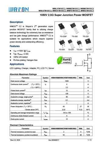
WM 2, WMN07N MM07N105C ML07N105C2 N105C2, WM C2 WMJ07N105C2, WM C2, WMP07N MK07N105C MO07N105C N105C2, WM C2 1050V Super Ju MOSFET V 2.0 S unction Power M T Descrip ption WMOSTM C2 is Wa 2nd generation super ayon s n junction MOSFET fa that is utilizing charge M amily S balance te or extremely esistance D echnology fo y low on-re S S G D D G G G and low
wmk037n10hgs.pdf
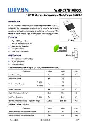
WMK037N10HGS 100V N-Channel Enhancement Mode Power MOSFET Description WMK037N10HGS uses Wayon's advanced power trench MOSFET technology that has been especially tailored to minimize the on-state resistance and yet maintain superior switching performance. This device is well suited for high efficiency fast switching applications. S Features D G TO-220 V = 100V, I = 170A
wmt07n10ts.pdf
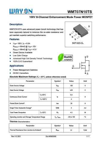
WMT07N10TS 100V N-Channel Enhancement Mode Power MOSFET Description WMT07N10TS uses advanced power trench technology that has been especially tailored to minimize the on-state resistance and yet maintain superior switching performance. Features V = 100V, I = 6.8A DS D R
wmll017n10hgs.pdf
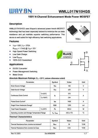
WMLL017N10HGS 100V N-Channel Enhancement Mode Power MOSFET Description D D WMLL017N10HGS uses Wayon's advanced power trench MOSFET S technology that has been especially tailored to minimize the on-state S G S S S S S S S S resistance and yet maintain superior switching performance. This S S G S S device is well suited for high efficiency fast switching applications.
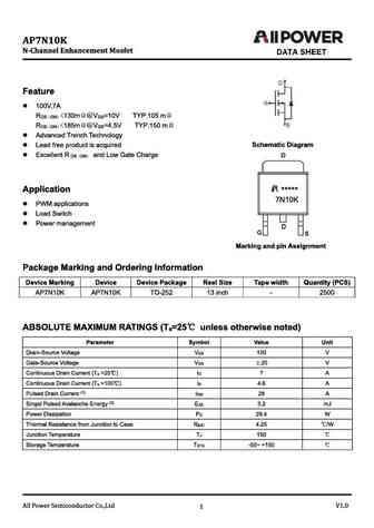
hgb037n10s hgk037n10s hgp037n10s.pdf
HGB037N10S HGK037N10S P-1 , HGP037N10S 100V N-Ch Power MOSFET Feature 100 V VDS High Speed Power Switching TO-263 2.8 RDS(on),typ m Enhanced Body diode dv/dt capability TO-247 3 RDS(on),typ m Enhanced Avalanche Ruggedness TO-220 3.1 RDS(on),typ m 100% UIS Tested, 100% Rg Tested 190 A ID (Sillicon Limited) Lead Free 120 A ID (Package Limited) Ap
hgb037n10t hgp037n10t hga037n10t.pdf
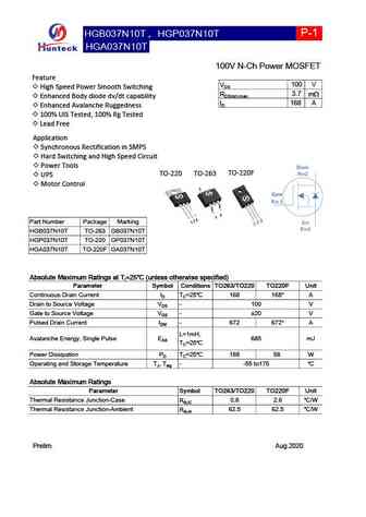
HGB037N10T HGP037N10T P-1 , HGA037N10T 100V N-Ch Power MOSFET Feature 100 V VDS High Speed Power Smooth Switching 3.7 RDS(on),max mW Enhanced Body diode dv/dt capability 168 A ID Enhanced Avalanche Ruggedness 100% UIS Tested, 100% Rg Tested Lead Free Application Synchronous Rectification in SMPS Hard Switching and High Speed Circuit Power Tools
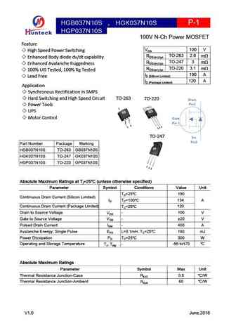
hgb017n10s.pdf
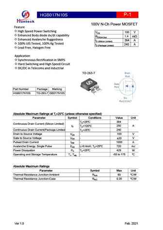
HGB017N10S P-1 100V N-Ch Power MOSFET Feature High Speed Power Switching 100 V VDS Enhanced Body diode dv/dt capability 1.4 RDS(on),typ mW Enhanced Avalanche Ruggedness 354 A ID (Sillicon Limited) 100% UIS Tested, 100% Rg Tested 240 A ID (Package Limited) Lead Free, Halogen Free Application Synchronous Rectification in SMPS Hard Switching and High S
hgn077n10sl.pdf
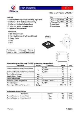
HGN077N10SL P-1 100V N-Ch Power MOSFET 100 V VDS Feature 6.4 RDS(on),typ VGS=10V m Optimized for high speed switching,Logic level 7.8 RDS(on),typ VGS=4.5V m Enhanced Body diode dv/dt capability 86 A ID (Sillicon Limited) Enhanced Avalanche Ruggedness 60 A ID (Package Limited) 100% UIS Tested, 100% Rg Tested Lead Free, Halogen Free Application DC-
hgb027n10a hgk027n10a hgp027n10a.pdf
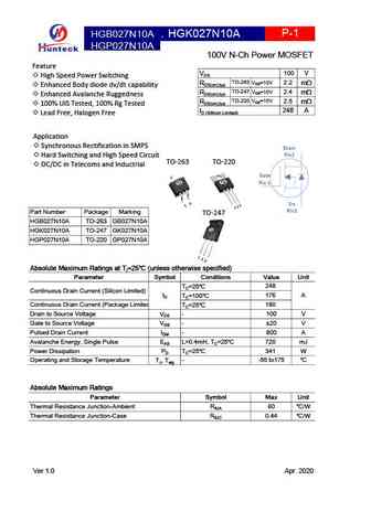
HGB027N10A , P-1 HGK027N10A HGP027N10A 100V N-Ch Power MOSFET Feature 100 V VDS High Speed Power Switching RDS(on),typ TO-263 VGS=10V 2.2 mW Enhanced Body diode dv/dt capability RDS(on),typ TO-247 VGS=10V 2.4 mW Enhanced Avalanche Ruggedness RDS(on),typ TO-220 VGS=10V 2.5 mW 100% UIS Tested, 100% Rg Tested 248 A ID (Sillicon Limited) Lead Free, Halogen Free
hgd077n10sl hgi077n10sl.pdf
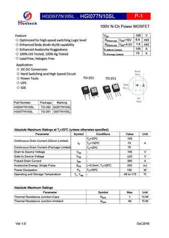
HGD077N10SL , HGI077N10SL P-1 100V N-Ch Power MOSFET 100 V VDS Feature 6.4 RDS(on),typ VGS=10V m Optimized for high speed switching,Logic level 7.8 RDS(on),typ VGS=4.5V m Enhanced Body diode dv/dt capability 105 A ID (Sillicon Limited) Enhanced Avalanche Ruggedness 70 A ID (Package Limited) 100% UIS Tested, 100% Rg Tested Lead Free, Halogen Free Appli
hgb027n10s hgk029n10s hgp030n10s.pdf
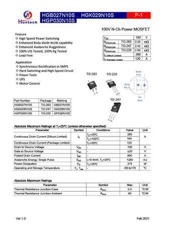
, P-1 HGB027N10S HGK029N10S HGP030N10S 100V N-Ch Power MOSFET Feature 100 V VDS High Speed Power Switching TO-263 2.25 RDS(on),typ mW Enhanced Body diode dv/dt capability TO-247 2.42 RDS(on),typ mW Enhanced Avalanche Ruggedness TO-220 2.50 RDS(on),typ mW 100% UIS Tested, 100% Rg Tested 260 A ID (Sillicon Limited) Lead Free 120 A ID (Package Limited) App
wsf07n10.pdf
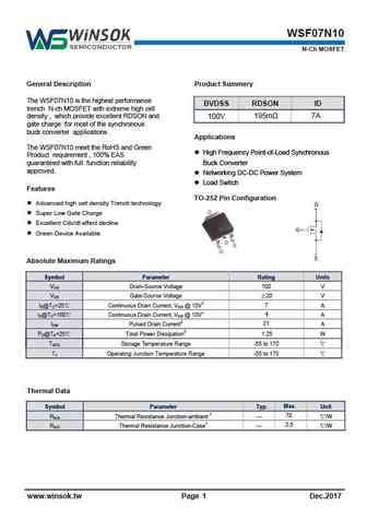
WSF07N10 N-Ch MOSFET Product Summery General Description The WSF07N10 is the highest performance BVDSS RDSON ID trench N-ch MOSFET with extreme high cell 195m 7A density , which provide excellent RDSON and 100V gate charge for most of the synchronous buck converter applications . Applications The WSF07N10 meet the RoHS and Green High Frequency Point-of-Load Synchronou
fqd7n10l.pdf
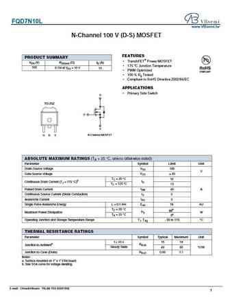
FQD7N10L www.VBsemi.tw N-Channel 100 V (D-S) MOSFET FEATURES PRODUCT SUMMARY TrenchFET Power MOSFET VDS (V) RDS(on) ( )ID (A) 175 C Junction Temperature 100 0.11 4 at VGS = 10 V 15 PWM Optimized 100 % Rg Tested Compliant to RoHS Directive 2002/95/EC APPLICATIONS Primary Side Switch D TO-252 G S G D S N-Channel MOSFET ABSOLUTE MAXIMUM RATINGS
hm17n10k.pdf
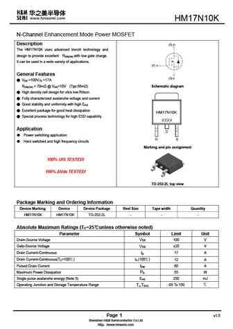
N-Channel Enhancement Mode Power MOSFET Description The uses advanced trench technology and design to provide excellent RDS(ON) with low gate charge. It can be used in a wide variety of applications. General Features VDS =100V,ID =17A RDS(ON)
sfd347n100c2.pdf
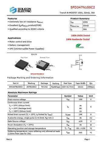
SFD347N100C2 Trench N-MOSFET 100V, 30m , 36A Features Product Summary Extremely low on-resistance RDS(on) VDS 100V Excellent QgxRDS(on) product(FOM) RDS(on) typ. 30m Qualified according to JEDEC criteria ID 36A 100% DVDS Tested Applications 100% Avalanche Tested Motor control and drive 100% Avalanche Tested 100% Avalanche Tested 100% Avalanche Tested 100%
sfp60n100 sfb60n100 sfp350n100c2 sfb347n100c2.pdf
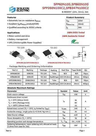
SFP60N100,SFB60N100 SFP350N100C2,SFB347N100C2 N-MOSFET 100V, 30m , 36A Features Product Summary Extremely low on-resistance RDS(on) VDS 100V Excellent QgxRDS(on) product(FOM) RDS(on) typ. 30m Qualified according to JEDEC criteria ID 36A Applications 100% DVDS Tested Motor control and drive 100% Avalanche Tested Battery management UPS (Uninterrupible
sfp080n100ac2 sfb077n100ac2.pdf
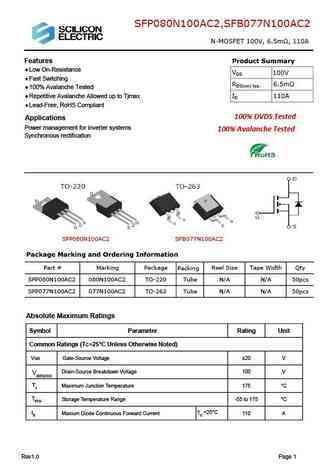
SFP080N100AC2,SFB077N100AC2 N-MOSFET 100V, 6.5m , 110A Features Product Summary Low On-Resistance VDS 100V Fast Switching RDS(on) typ. 6.5m 100% Avalanche Tested Repetitive Avalanche Allowed up to Tjmax ID 110A Lead-Free, RoHS Compliant 100% DVDS Tested Applications Power management for inverter systems 100% Avalanche Tested Synchronous rectification SFP08
sfp040n100c3 sfb037n100c3.pdf
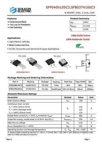
SFP040N100C3,SFB037N100C3 N-MOSFET 100V, 3.2m , 120A Features Product Summary Enhancement Mode VDS 100V Very Low On-Resistance RDS(on) 3.2m Fast Switching ID 120A 100% DVDS Tested Applications 100% Avalanche Tested Light Electric Vehicles Motor Control and Drive DC/DC Converter,and Genneral Purpose Applications SFP040N100C3 SFB037N100C3 Package Mark
sfp030n100c3 sfb027n100c3.pdf
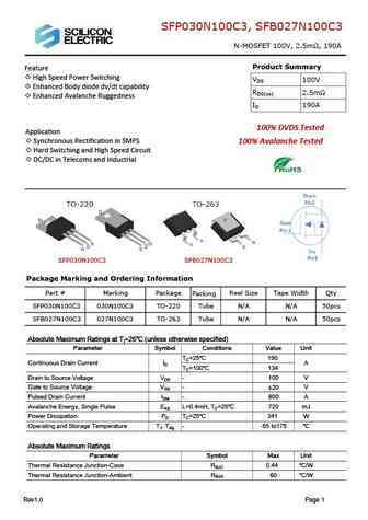
SFP030N100C3, SFB027N100C3 N-MOSFET 100V, 2.5m , 190A Product Summary Feature High Speed Power Switching VDS 100V Enhanced Body diode dv/dt capability RDS(on) 2.5m Enhanced Avalanche Ruggedness ID 190A 100% DVDS Tested Application Synchronous Rectification in SMPS 100% Avalanche Tested Hard Switching and High Speed Circuit 100% Avalanche Tested 100%
sfw027n100c3.pdf
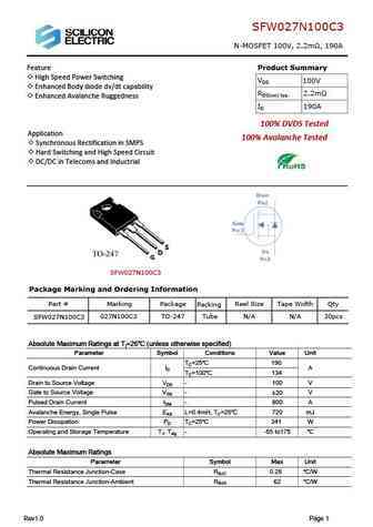
SFW027N100C3 N-MOSFET 100V, 2.2m , 190A Feature Product Summary High Speed Power Switching VDS 100V Enhanced Body diode dv/dt capability RDS(on) typ. 2.2m Enhanced Avalanche Ruggedness ID 190A 100% DVDS Tested Application 100% Avalanche Tested Synchronous Rectification in SMPS Hard Switching and High Speed Circuit DC/DC in Telecoms and Inductrial D
fxn07n10ns.pdf
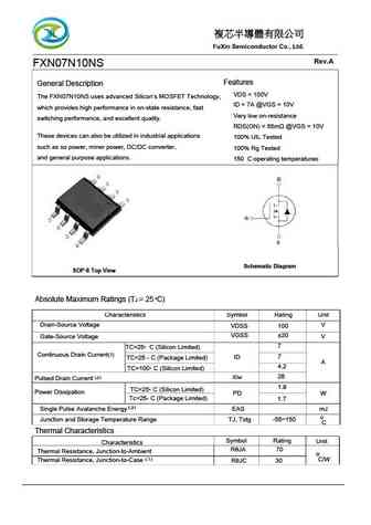
FuXin Semiconductor Co., Ltd. Rev.A FXN07N10NS Features General Description The FXN07N10NS uses advanced Silicon s MOSFET Technology, VDS = 100V ID = 7A @VGS = 10V which provides high performance in on-state resistance, fast Very low on-resistance switching performance, and excellent quality. RDS(ON)
ipb027n10n5.pdf
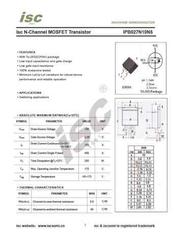
Isc N-Channel MOSFET Transistor IPB027N10N5 FEATURES With To-263(D2PAK) package Low input capacitance and gate charge Low gate input resistance 100% avalanche tested Minimum Lot-to-Lot variations for robust device performance and reliable operation APPLICATIONS Switching applications ABSOLUTE MAXIMUM RATINGS(T =25 ) a SYMBOL PARAMETER VALUE UNIT V Drain-Source V
ipb027n10n3.pdf

Isc N-Channel MOSFET Transistor IPB027N10N3 FEATURES With To-263(D2PAK) package Low input capacitance and gate charge Low gate input resistance 100% avalanche tested Minimum Lot-to-Lot variations for robust device performance and reliable operation APPLICATIONS Switching applications ABSOLUTE MAXIMUM RATINGS(T =25 ) a SYMBOL PARAMETER VALUE UNIT V Drain-Source V
Другие IGBT... 25N10, 30N06, 50N06, 60N06, 60N08, 6N10, 70N06, 75N75, AOD4184A, 7N10Z, 80N08, UF1010A, UF1010E, UF3710, UF4N20, UF540, UF630
🌐 : EN ES РУ

Список транзисторов
Обновления
MOSFET: AUW033N08BG | AUW025N10 | AUR030N10 | AUR020N10 | AUR020N085 | AUR014N10 | AUP074N10 | AUP065N10 | AUP062N08BG | AUP060N08AG | HYG053N10NS1B | HYG053N10NS1P | AP220N04T | AP220N04P | QM3126M3 | AUP060N055
Popular searches
ksc2383 datasheet | 2n3906 equivalent | a733 transistor equivalent | 2n5401 transistor datasheet | 2n2222 data sheet | irf3205 datasheet | oc71 | njw0302g