Аналоги 12P10. Основные параметры
Наименование производителя: 12P10
Тип транзистора: MOSFET
Полярность: P
Pd ⓘ - Максимальная рассеиваемая мощность: 65
W
|Vds|ⓘ - Предельно допустимое напряжение сток-исток: 100
V
|Vgs|ⓘ - Предельно допустимое напряжение затвор-исток: 30
V
|Id| ⓘ - Максимально
допустимый постоянный ток стока: 9.4
A
Tj ⓘ - Максимальная температура канала: 150
°C
tr ⓘ -
Время нарастания: 160
ns
Cossⓘ - Выходная емкость: 220
pf
Rds ⓘ - Сопротивление сток-исток открытого транзистора: 0.24
Ohm
Тип корпуса:
TO-263
SOP-8
TO-251
TO-252
SOT-223
TO-220
Аналог (замена) для 12P10
-
подбор ⓘ MOSFET транзистора по параметрам
12P10 даташит
..1. Size:259K utc
12p10.pdf 
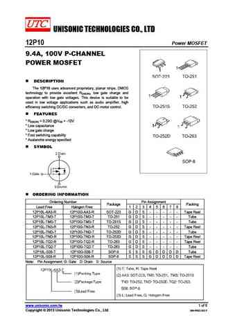
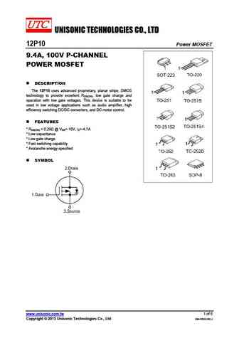
UNISONIC TECHNOLOGIES CO., LTD 12P10 Power MOSFET 9.4A, 100V P-CHANNEL POWER MOSFET DESCRIPTION The 12P10 uses advanced proprietary, planar stripe, DMOS technology to provide excellent RDS(ON), low gate charge and operation with low gate voltages. This device is suitable to be used in low voltage applications such as audio amplifier, high efficiency switching DC/DC converte
..2. Size:1653K goford
12p10.pdf 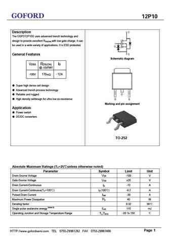
GOFORD 12P10 Description The OGFD12P10G uses advanced trench technology and design to provide excellent RDS(ON) with low gate charge. It can be used in a wide variety of applications. It is ESD protested. General Features Schematic diagram VDSS RDS(ON) ID @ (typ) -10V -100V 170m - 12A Super high dense cell design Advanced trench process technology Reliable
0.2. Size:164K motorola
mtp12p10.pdf 
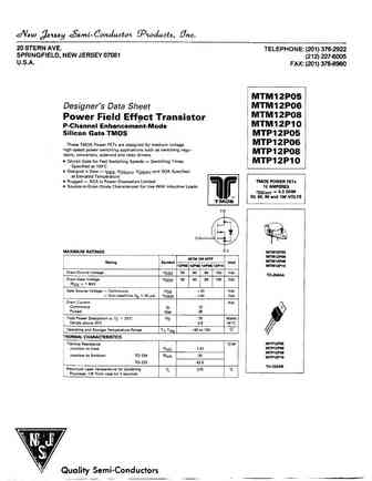
MOTOROLA Order this document SEMICONDUCTOR TECHNICAL DATA by MTP12P10/D Designer's Data Sheet MTP12P10 Power Field Effect Transistor P Channel Enhancement Mode Silicon Gate This TMOS Power FET is designed for medium voltage, high TMOS POWER FET speed power switching applications such as switching regulators, 12 AMPERES converters, solenoid and relay drivers. 100 VOLTS S
0.3. Size:190K motorola
mtp12p10rev1a.pdf 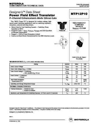
MOTOROLA Order this document SEMICONDUCTOR TECHNICAL DATA by MTP12P10/D Designer's Data Sheet MTP12P10 Power Field Effect Transistor P Channel Enhancement Mode Silicon Gate This TMOS Power FET is designed for medium voltage, high TMOS POWER FET speed power switching applications such as switching regulators, 12 AMPERES converters, solenoid and relay drivers. 100 VOLTS S
0.4. Size:457K st
strh12p10.pdf 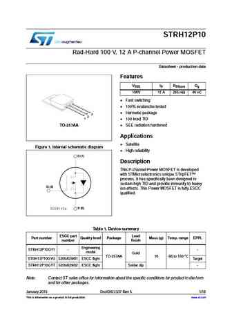
STRH12P10 Rad-Hard 100 V, 12 A P-channel Power MOSFET Datasheet - production data Features VDSS ID RDS(on) Qg 100V 12 A 265 m 40 nC Fast switching 100% avalanche tested Hermetic package 3 2 1 100 krad TID TO-257AA SEE radiation hardened Applications Satellite Figure 1. Internal schematic diagram High reliability D (1) Description This P-channel
0.5. Size:877K fairchild semi
fqd12p10tm f085.pdf 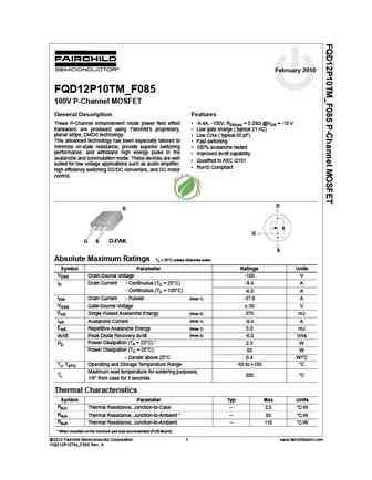
February 2010 tm FQD12P10TM_F085 100V P-Channel MOSFET General Description Features These P-Channel enhancement mode power field effect -9.4A, -100V, RDS(on) = 0.29 @VGS = -10 V transistors are produced using Fairchild s proprietary, Low gate charge ( typical 21 nC) planar stripe, DMOS technology. Low Crss ( typical 65 pF) This advanced technology has been especially t
0.6. Size:634K fairchild semi
fqb12p10tm.pdf 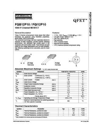
TM QFET FQB12P10 / FQI12P10 100V P-Channel MOSFET General Description Features These P-Channel enhancement mode power field effect -11.5A, -100V, RDS(on) = 0.29 @VGS = -10 V transistors are produced using Fairchild s proprietary, Low gate charge ( typical 21 nC) planar stripe, DMOS technology. Low Crss ( typical 65 pF) This advanced technology has been especially tailo
0.7. Size:666K fairchild semi
fqd12p10tf fqd12p10tm.pdf 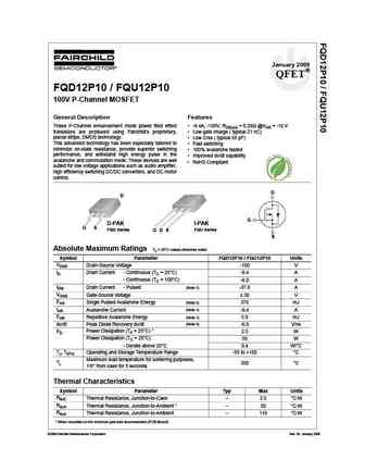
January 2009 QFET FQD12P10 / FQU12P10 100V P-Channel MOSFET General Description Features These P-Channel enhancement mode power field effect -9.4A, -100V, RDS(on) = 0.29 @VGS = -10 V transistors are produced using Fairchild s proprietary, Low gate charge ( typical 21 nC) planar stripe, DMOS technology. Low Crss ( typical 65 pF) This advanced technology has been espec
0.8. Size:629K fairchild semi
fqpf12p10.pdf 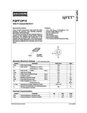
TM QFET FQPF12P10 100V P-Channel MOSFET General Description Features These P-Channel enhancement mode power field effect -8.2A, -100V, RDS(on) = 0.29 @VGS = -10 V transistors are produced using Fairchild s proprietary, Low gate charge ( typical 21 nC) planar stripe, DMOS technology. Low Crss ( typical 65 pF) This advanced technology has been especially tailored to
0.9. Size:359K fairchild semi
rfp12p08 rfp12p10.pdf 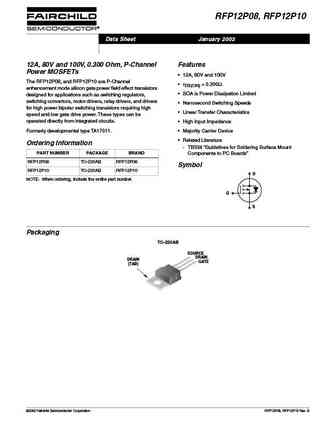
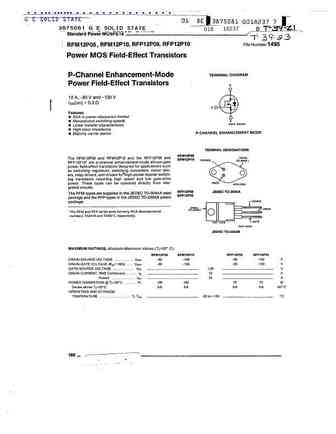
RFP12P08, RFP12P10 Data Sheet January 2002 12A, 80V and 100V, 0.300 Ohm, P-Channel Features Power MOSFETs 12A, 80V and 100V The RFP12P08, and RFP12P10 are P-Channel rDS(ON) = 0.300 enhancement mode silicon gate power field effect transistors SOA is Power Dissipation Limited designed for applications such as switching regulators, switching convertors, motor drivers, r
0.10. Size:1058K fairchild semi
fqp12p10.pdf 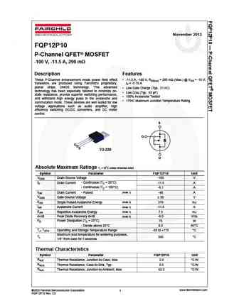
November 2013 FQP12P10 P-Channel QFET MOSFET -100 V, -11.5 A, 290 m Description Features These P-Channel enhancement mode power field effect -11.5 A, -100 V, RDS(on) = 290 m (Max.) @ VGS = -10 V, transistors are produced using Fairchild s proprietary, ID = -5.75 A planar stripe, DMOS technology. This advanced Low Gate Charge (Typ. 21 nC) technology has been especial
0.12. Size:894K mcc
mcu12p10.pdf 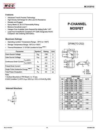
MCU12P10 Features Advanced Trench Process Technology High Density Cell Design for Ultra Low On-Resistance Reliable and Rugged Epoxy Meets UL 94 V-0 Flammability Rating P-CHANNEL Moisture Sensitivity Level 1 MOSFET Halogen Free Available Upon Request By Adding Suffix "-HF" Lead Free Finish/RoHS Compliant ("P" Suffix Designates RoHS Compliant. See Ordering In
0.13. Size:72K onsemi
mtp12p10-d mtp12p10g.pdf 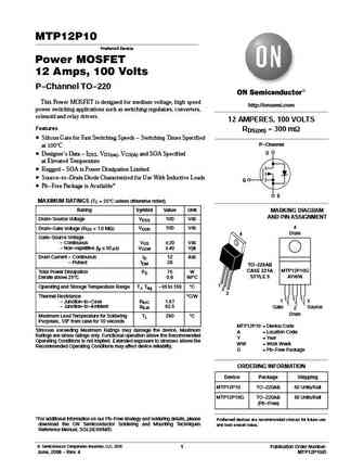
MTP12P10 Preferred Device Power MOSFET 12 Amps, 100 Volts P-Channel TO-220 This Power MOSFET is designed for medium voltage, high speed http //onsemi.com power switching applications such as switching regulators, converters, solenoid and relay drivers. 12 AMPERES, 100 VOLTS Features RDS(on) = 300 mW Silicon Gate for Fast Switching Speeds - Switching Times Specified P-Channel a
0.17. Size:280K utc
utt12p10.pdf 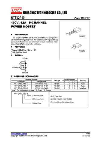
UNISONIC TECHNOLOGIES CO., LTD UTT12P10 Power MOSFET 100V, 12A P-CHANNEL POWER MOSFET DESCRIPTION The UTC UTT12P10 is a P-channel power MOSFET using UTC s advanced technology to provide the customers with high switching speed, cost-effectiveness and a minimum on-state resistance. It can also withstand high energy in the avalanche. FEATURES * RDS(ON)
0.19. Size:401K secos
ssd12p10.pdf 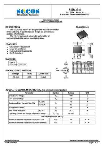
SSD12P10 2A , 650V , RDS(ON) 8 P-Channel Enhancement MOSFET Elektronische Bauelemente RoHS Compliant Product A suffix of -C specifies halogen free TO-252(D-Pack) DESCRIPTION The SSD12P10 provide the designer with the best combination of fast switching, ruggedized device design, low on-resistance and cost-effectiveness. The TO-252 package is universally preferred f
0.20. Size:252K cet
ced12p10 ceu12p10.pdf 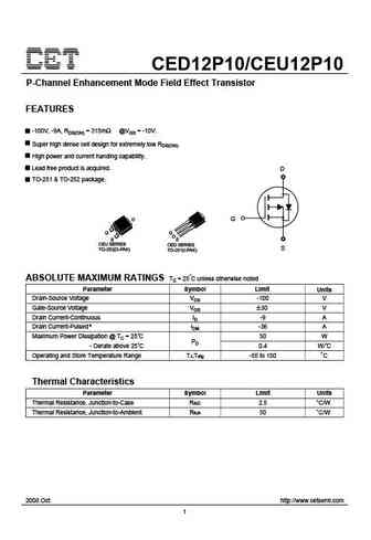
CED12P10/CEU12P10 P-Channel Enhancement Mode Field Effect Transistor FEATURES -100V, -9A, RDS(ON) = 315m @VGS = -10V. Super high dense cell design for extremely low RDS(ON). High power and current handing capability. Lead free product is acquired. D TO-251 & TO-252 package. D G G S CEU SERIES CED SERIES S TO-252(D-PAK) TO-251(I-PAK) ABSOLUTE MAXIMUM RATINGS Tc = 25 C unless
0.21. Size:126K cet
cep12p10 ceb12p10.pdf 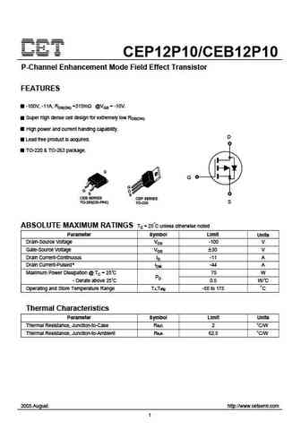
CEP12P10/CEB12P10 P-Channel Enhancement Mode Field Effect Transistor FEATURES -100V, -11A, RDS(ON) =315m @VGS = -10V. Super high dense cell design for extremely low RDS(ON). High power and current handing capability. D Lead free product is acquired. TO-220 & TO-263 package. G CEB SERIES CEP SERIES TO-263(DD-PAK) S TO-220 ABSOLUTE MAXIMUM RATINGS Tc = 25 C unless otherwise noted
0.22. Size:834K goford
g12p10k.pdf 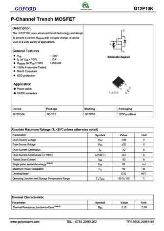
GOFORD G12P10K P-Channel Trench MOSFET Description The G12P10K uses advanced trench technology and design to provide excellent RDS(ON) with low gate charge. It can be used in a wide variety of applications. General Features VDS -100V Schematic diagram - ID (at VGS = 10V) -12A - RDS(ON) (at VGS = 10V)
0.23. Size:2919K kexin
fqd12p10.pdf 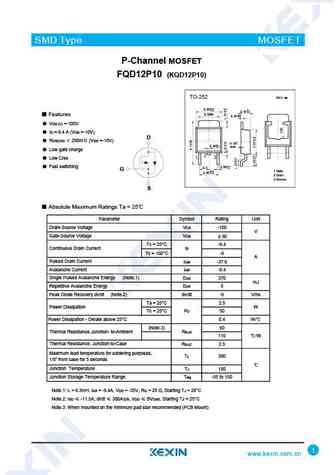
SMD Type MOSFET P-Channel MOSFET FQD12P10 (KQD12P10) TO-252 Unit mm +0.15 6.50-0.15 +0.1 2.30 -0.1 +0.2 5.30-0.2 +0.8 Features 0.50 -0.7 VDS (V) =-100V ID =-9.4 A (VGS =-10V) D RDS(ON) 290m (VGS =-10V) 0.127 +0.1 0.80-0.1 max Low gate charge Low Crss + 0.1 Fast switching 2.3 0.60- 0.1 G +0.15 4 .60 -0.15 S Absolute Maximu
0.24. Size:69K chenmko
chm12p10ngp.pdf 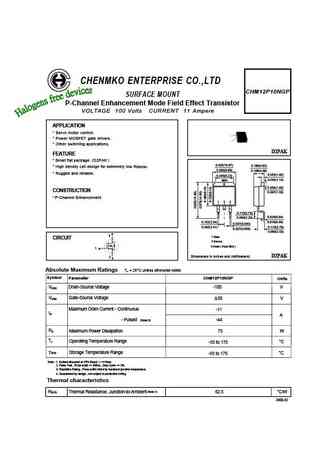
CHENMKO ENTERPRISE CO.,LTD CHM12P10N SURFACE MOUNT P-Channel Enhancement Mode Field Effect Transistor VOLTAGE 100 Volts CURRENT 11 Ampere APPLICATION * Servo motor control. * Power MOSFET gate drivers. * Other switching applications. D2PAK FEATURE * Small flat package. (D2PAK ) 0.420(10.67) 0.190(4.83) * High density cell design for extremely low RDS(ON). 0.380(9.69) 0.160
0.25. Size:607K way-on
wmq12p10ts.pdf 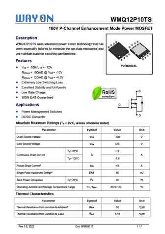
WMQ12P10TS 100V P-Channel Enhancement Mode Power MOSFET Description D D D D WMQ12P10TS uses advanced power trench technology that has D D D D been especially tailored to minimize the on-state resistance and yet maintain superior switching performance. S G S S S S G S Features PDFN3030-8L V = -100V, I = -12A DS D R
0.26. Size:1087K cn vbsemi
vbzfb12p10.pdf 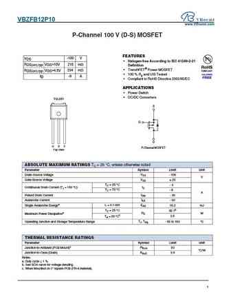
VBZFB12P10 www.VBsemi.com P-Channel 100 V (D-S) MOSFET FEATURES -100 V VDS Halogen-free According to IEC 61249-2-21 m RDS(on),typ VGS=10V 215 Definition TrenchFET Power MOSFET RDS(on),typ VGS=4.5V 234 m 100 % Rg and UIS Tested A ID -9 Compliant to RoHS Directive 2002/95/EC APPLICATIONS Power Switch DC/DC Converters TO-251 S G D G D S P-Cha
0.27. Size:834K cn vbsemi
vbze12p10.pdf 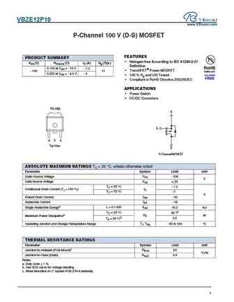
VBZE12P10 www.VBsemi.com P-Channel 100 V (D-S) MOSFET FEATURES PRODUCT SUMMARY Halogen-free According to IEC 61249-2-21 VDS (V) RDS(on) ( ) ID (A) Qg (Typ.) Definition 0.180 at VGS = - 10 V - 7.5 TrenchFET Power MOSFET - 100 11 0.200 at VGS = - 4.5 V - 6 100 % Rg and UIS Tested Compliant to RoHS Directive 2002/95/EC APPLICATIONS Power Switch DC/DC Con
0.28. Size:911K cn vbsemi
ssd12p10.pdf 
SSD12P10 www.VBsemi.tw P-Channel 100 V (D-S) MOSFET FEATURES PRODUCT SUMMARY Halogen-free According to IEC 61249-2-21 VDS (V) RDS(on) ( ) ID (A) Qg (Typ.) Definition 0.250 at VGS = - 10 V - 8.8 TrenchFET Power MOSFET - 100 11.7 0.280 at VGS = - 4.5 V - 8.0 100 % Rg and UIS Tested Compliant to RoHS Directive 2002/95/EC APPLICATIONS TO-251 Power Switch
0.29. Size:841K cn vbsemi
vbzm12p10.pdf 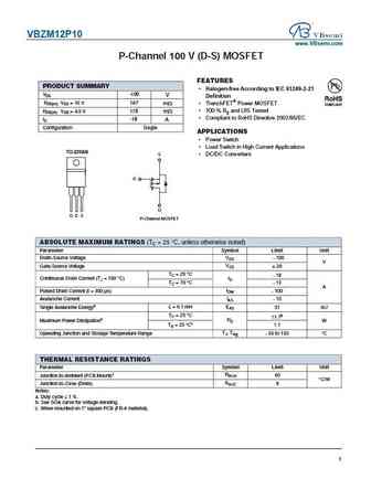
VBZM12P10 www.VBsemi.com P-Channel 100 V (D-S) MOSFET FEATURES PRODUCT SUMMARY Halogen-free According to IEC 61249-2-21 VDS -100 V Definition RDS(on) VGS = 10 V 167 m TrenchFET Power MOSFET 100 % Rg and UIS Tested RDS(on) VGS = 4.5 V 178 m Compliant to RoHS Directive 2002/95/EC ID -18 A Configuration Single APPLICATIONS Power Switch Load Switch
0.30. Size:777K cn vbsemi
fqd12p10.pdf 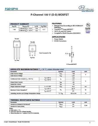
FQD12P10 www.VBsemi.tw P-Channel 100 V (D-S) MOSFET FEATURES PRODUCT SUMMARY Halogen-free According to IEC 61249-2-21 VDS (V) RDS(on) ( ) ID (A) Qg (Typ.) Definition 0.250 at VGS = - 10 V - 8.8 TrenchFET Power MOSFET - 100 11.7 0.280 at VGS = - 4.5 V - 8.0 100 % Rg and UIS Tested Compliant to RoHS Directive 2002/95/EC APPLICATIONS TO-251 Power Switch
Другие MOSFET... UF630
, UF640
, UF6N15
, UF8010
, UFZ44
, URFP150
, UT12N10
, UT2N10
, IRF640
, 7P20
, UF9640
, UF9Z24
, UT2955
, UTT120P06
, UTT12P10
, UTT16P10
, UTT18P10
.