AO3424 - Аналоги. Основные параметры
Наименование производителя: AO3424
Тип транзистора: MOSFET
Полярность: N
Pd ⓘ - Максимальная рассеиваемая мощность: 1.4
W
|Vds|ⓘ - Предельно допустимое напряжение сток-исток: 30
V
|Vgs|ⓘ - Предельно допустимое напряжение затвор-исток: 12
V
|Id| ⓘ - Максимально
допустимый постоянный ток стока: 3.8
A
Tj ⓘ - Максимальная температура канала: 150
°C
tr ⓘ -
Время нарастания: 1.5
ns
Cossⓘ - Выходная емкость: 35
pf
Rds ⓘ - Сопротивление сток-исток открытого транзистора: 0.055
Ohm
Тип корпуса:
SOT23
Аналог (замена) для AO3424
AO3424 технические параметры
..1. Size:449K aosemi
ao3424.pdf 

AO3424 30V N-Channel MOSFET General Description Product Summary VDS 30V The AO3424 uses advanced trench technology to provide excellent RDS(ON), low gate charge and operation with gate ID (at VGS=10V) 3.8A voltages as low as 2.5V. This device is suitable for use as RDS(ON) (at VGS=10V)
..2. Size:1795K kexin
ao3424.pdf 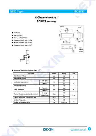
SMD Type MOSFET N-Channel MOSFET AO3424 (KO3424) SOT-23 Unit mm +0.1 2.9 -0.1 +0.1 0.4-0.1 3 Features VDS (V) = 30V ID = 3.8 A (VGS = 10 V) 1 2 RDS(ON) 55m (VGS = 10V) +0.1 +0.05 0.95 -0.1 0.1 -0.01 +0.1 1.9 -0.1 RDS(ON) 65m (VGS = 4.5V) RDS(ON) 85m (VGS = 2.5V) 1. Gate 2. Source D D 3. Drain G G S S Absolute Ma
..3. Size:459K cn shikues
ao3424.pdf 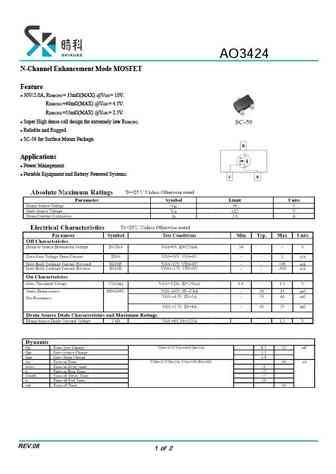
AO3424 N-Channel Enhancement Mode MOSFET Channel Enhancement Mode MOSFET Channel Enhancement Mode MOSFET Channel Enhancement Mode MOSFET Channel Enhancement Mode MOSFET Feature Feature 30V/2.0A, RDS(ON) = 35m (MAX) @V = 10V. 30V/2.0A, RDS(ON) = 35m (MAX) @VGS = 10V. RDS(ON) =40m (MAX) @VGS = 4.5V. DS(ON) =40m (MAX) @V = 4.5V. RDS(ON) =55m (MAX) @VGS = 2.5V. DS(ON) =5
0.1. Size:1799K kexin
ao3424-3.pdf 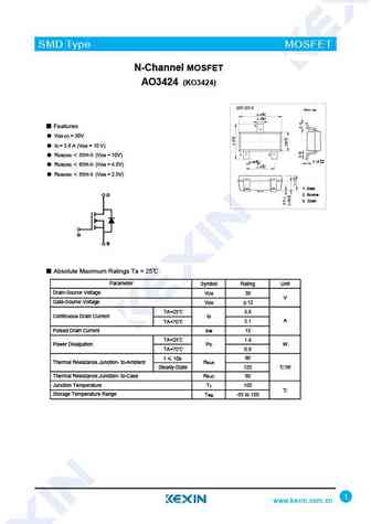
SMD Type MOSFET N-Channel MOSFET AO3424 (KO3424) SOT-23-3 Unit mm +0.2 2.9 -0.1 +0.1 0.4 -0.1 3 Features VDS (V) = 30V ID = 3.8 A (VGS = 10 V) 1 2 RDS(ON) 55m (VGS = 10V) +0.02 +0.1 0.15 -0.02 0.95-0.1 RDS(ON) 65m (VGS = 4.5V) +0.1 1.9 -0.2 RDS(ON) 85m (VGS = 2.5V) 1. Gate 2. Source D D 3. Drain G G S S Absolute
9.1. Size:282K aosemi
ao3423.pdf 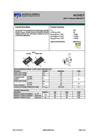
AO3423 20V P-Channel MOSFET General Description Product Summary VDS -20V The AO3423 uses advanced trench technology to provide excellent RDS(ON), low gate charge and operation with gate ID (at VGS=-10V) -2A voltages as low as 2.5V. This device is suitable for use as RDS(ON) (at VGS= -10V)
9.2. Size:317K aosemi
ao3420.pdf 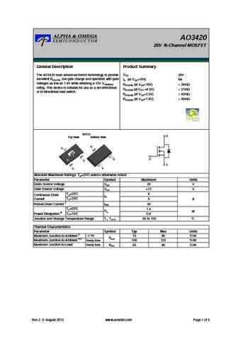
AO3420 20V N-Channel MOSFET General Description Product Summary VDS 20V The AO3420 uses advanced trench technology to provide excellent RDS(ON), low gate charge and operation with gate ID (at VGS=10V) 6A voltages as low as 1.8V while retaining a 12V VGS(MAX) RDS(ON) (at VGS=10V)
9.3. Size:177K aosemi
ao3422.pdf 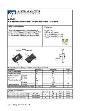
AO3422 N-Channel Enhancement Mode Field Effect Transistor General Description Features The AO3422 uses advanced trench technology to VDS (V) = 55V provide excellent RDS(ON) and low gate charge. It offers ID = 2.1A (VGS = 4.5V) operation over a wide gate drive range from 2.5V to RDS(ON)
9.4. Size:309K aosemi
ao3421e.pdf 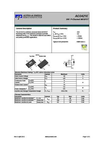
AO3421E 30V P-Channel MOSFET General Description Product Summary VDS The AO3421E combines advanced trench MOSFET -30V technology with a low resistance package to provide ID (at VGS=-10V) -3A extremely low RDS(ON). This device is ideal for load switch RDS(ON) (at VGS=-10V)
9.5. Size:234K aosemi
ao3421.pdf 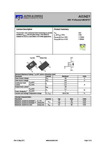
AO3421 30V P-Channel MOSFET General Description Product Summary VDS -30V The AO3421 uses advanced trench technology to provide excellent RDS(ON) and low gate charge. This device is ID (at VGS=-10V) -2.6A suitable for use as a load switch or in PWM applications. RDS(ON) (at VGS=-10V)
9.6. Size:717K shenzhen
ao3423.pdf 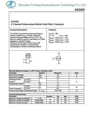
Shenzhen Tuofeng Semiconductor Technology Co., Ltd AO3423 AO3423 P-Channel Enhancement Mode Field Effect Transistor General Description Features The AO3423 uses advanced trench technology to VDS (V) = -20V provide excellent RDS(ON), low gate charge and ID = -2 A (VGS = -10V) operation with gate voltages as low as 2.5V. This RDS(ON)
9.7. Size:489K shenzhen
ao3420.pdf 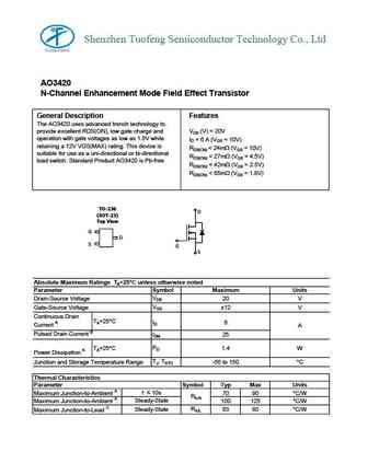
Shenzhen Tuofeng Semiconductor Technology Co., Ltd AO3420 N-Channel Enhancement Mode Field Effect Transistor General Description Features The AO3420 uses advanced trench technology to provide excellent RDS(ON), low gate charge and VDS (V) = 20V operation with gate voltages as low as 1.8V while ID = 6 A (VGS = 10V) retaining a 12V VGS(MAX) rating. This device is RDS(ON)
9.8. Size:256K shenzhen
ao3422.pdf 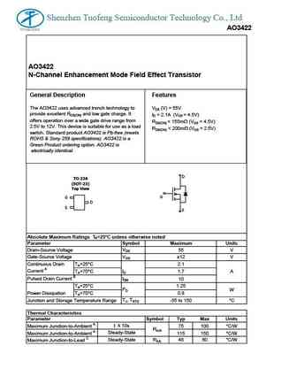
Shenzhen Tuofeng Semiconductor Technology Co., Ltd AO3422 AO3422 N-Channel Enhancement Mode Field Effect Transistor General Description Features The AO3422 uses advanced trench technology to VDS (V) = 55V provide excellent RDS(ON) and low gate charge. It ID = 2.1A (VGS = 4.5V) offers operation over a wide gate drive range from RDS(ON)
9.9. Size:1856K kexin
ao3421e-3.pdf 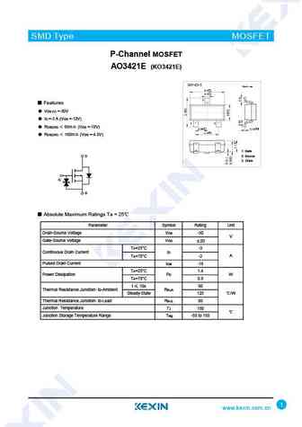
SMD Type MOSFET P-Channel MOSFET AO3421E (KO3421E) SOT-23-3 Unit mm +0.2 2.9-0.1 +0.1 0.4 -0.1 3 Features VDS (V) =-30V ID =-3 A (VGS =-10V) 1 2 RDS(ON) 95m (VGS =-10V) +0.02 +0.1 0.15 -0.02 0.95 -0.1 +0.1 1.9 -0.2 RDS(ON) 160m (VGS =-4.5V) 1. Gate D 2. Source 3. Drain G S Absolute Maximum Ratings Ta = 25 Parameter Symbol R
9.10. Size:1760K kexin
ao3423.pdf 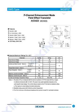
SMD Type AO3423 (KO3423) SOT-23 Unit mm +0.2 2.9-0.2 +0.1 0.4 -0.05 3 1 2 +0.1 +0.05 0.95 -0.1 0.1 -0.01 1.9+0.2 -0.2 D ESD Rating 2000V HBM G 1. Gate 2. Source 3. Drain S 0.4 +0.2 +0.2 2.8 -0.2 1.6 -0.1 0.55 +0.2 1.1 -0.1 +0.1 0-0.1 0.38 -0.1 SMD Type AO3423 (KO3423) Testconditions AS* SMD Type AO3423 (KO3423) 10 15 -10.0V -4.0V VDS=-5V -8
9.11. Size:1076K kexin
ao3422-3.pdf 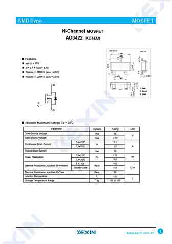
SMD Type MOSFET N-Channel MOSFET AO3422 (KO3422) SOT-23-3 Unit mm +0.2 2.9-0.1 +0.1 0.4 -0.1 Features 3 VDS (V) = 55V ID = 2.1 A (VGS = 4.5V) RDS(ON) 160m (VGS = 4.5V) 1 2 +0.02 +0.1 0.15 -0.02 0.95 -0.1 RDS(ON) 200m (VGS = 2.5V) +0.1 1.9 -0.2 D 1. Gate 2. Source 3. Drain G S Absolute Maximum Ratings Ta = 25 Parameter Symb
9.12. Size:1825K kexin
ao3420.pdf 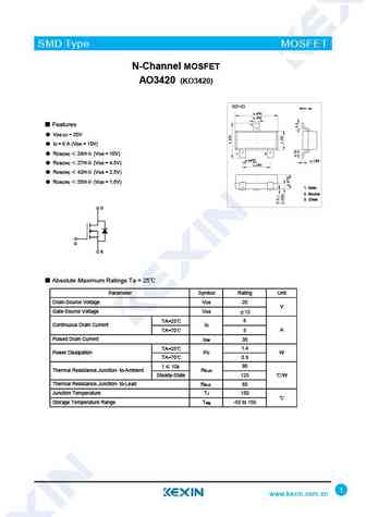
SMD Type MOSFET N-Channel MOSFET AO3420 (KO3420) SOT-23 Unit mm +0.1 2.9-0.1 +0.1 0.4 -0.1 3 Features VDS (V) = 20V ID = 6 A (VGS = 10V) 1 2 RDS(ON) 24m (VGS = 10V) +0.1 0.95-0.1 0.1+0.05 -0.01 RDS(ON) 27m (VGS = 4.5V) 1.9+0.1 -0.1 RDS(ON) 42m (VGS = 2.5V) RDS(ON) 55m (VGS = 1.8V) 1. Gate 2. Source 3. Drain D
9.13. Size:1969K kexin
ao3423-3.pdf 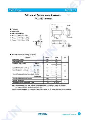
SMD Type MOSFET P-Channel Enhancement MOSFET AO3423 (KO3423) SOT-23-3 Unit mm +0.2 2.9-0.1 +0.1 0.4 -0.1 3 Features VDS (V) =-20V ID =-2.0 A (VGS =-10V) D 1 2 RDS(ON) 92m (VGS =-10V) +0.02 +0.1 0.15 -0.02 0.95 -0.1 RDS(ON) 118m (VGS =-4.5V) +0.1 1.9 -0.2 RDS(ON) 166m (VGS =-2.5V) G 1. Gate 2. Source 3. Drain S Abso
9.14. Size:963K kexin
ao3422.pdf 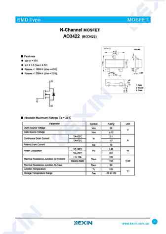
SMD Type MOSFET N-Channel MOSFET AO3422 (KO3422) SOT-23 Unit mm +0.1 2.9-0.1 +0.1 0.4 -0.1 Features 3 VDS (V) = 55V ID = 2.1 A (VGS = 4.5V) RDS(ON) 160m (VGS = 4.5V) 1 2 +0.05 0.95+0.1 -0.1 0.1 -0.01 RDS(ON) 200m (VGS = 2.5V) 1.9+0.1 -0.1 D 1. Gate 2. Source 3. Drain G S Absolute Maximum Ratings Ta = 25 Parameter Symbol Rat
9.15. Size:1833K kexin
ao3420-3.pdf 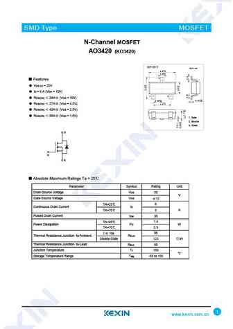
SMD Type MOSFET N-Channel MOSFET AO3420 (KO3420) SOT-23-3 Unit mm +0.2 2.9 -0.1 +0.1 0.4-0.1 3 Features VDS (V) = 20V ID = 6 A (VGS = 10V) 1 2 RDS(ON) 24m (VGS = 10V) +0.02 +0.1 0.15 -0.02 0.95 -0.1 +0.1 RDS(ON) 27m (VGS = 4.5V) 1.9 -0.2 RDS(ON) 42m (VGS = 2.5V) RDS(ON) 55m (VGS = 1.8V) 1. Gate 2. Source 3. Drai
9.16. Size:1703K kexin
ao3421e.pdf 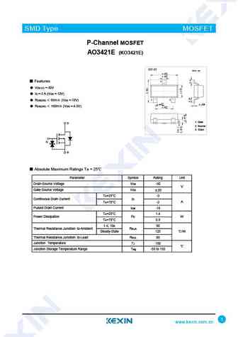
SMD Type MOSFET P-Channel MOSFET AO3421E (KO3421E) SOT-23 Unit mm +0.1 2.9-0.1 +0.1 0.4 -0.1 3 Features VDS (V) =-30V ID =-3 A (VGS =-10V) 1 2 RDS(ON) 95m (VGS =-10V) +0.1 0.95-0.1 0.1+0.05 -0.01 RDS(ON) 160m (VGS =-4.5V) +0.1 1.9-0.1 1. Gate D 2. Source 3. Drain G S Absolute Maximum Ratings Ta = 25 Parameter Symbol Rating
9.17. Size:1179K kexin
ao3421-3.pdf 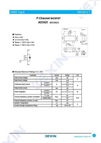
SMD Type MOSFET P-Channel MOSFET AO3421 (KO3421) SOT-23-3 Unit mm +0.2 2.9 -0.1 +0.1 0.4-0.1 3 Features VDS (V) =-30V ID =-2.6 A (VGS =-10V) 1 2 RDS(ON) 110m (VGS =-10V) +0.02 +0.1 0.15 -0.02 0.95 -0.1 +0.1 RDS(ON) 180m (VGS =-4.5V) 1.9 -0.2 D 1. Gate 2. Source 3. Drain G S Absolute Maximum Ratings Ta = 25 Parameter Symbol
9.18. Size:1030K kexin
ao3421.pdf 
SMD Type MOSFET P-Channel MOSFET AO3421 (KO3421) SOT-23 Unit mm +0.1 2.9 -0.1 +0.1 0.4-0.1 Features 3 VDS (V) =-30V ID =-2.6 A (VGS =-10V) RDS(ON) 110m (VGS =-10V) 1 2 +0.1 +0.05 0.95 -0.1 0.1 -0.01 RDS(ON) 180m (VGS =-4.5V) +0.1 1.9 -0.1 D 1. Gate 2. Source 3. Drain G S Absolute Maximum Ratings Ta = 25 Parameter Symbol Ratin
9.19. Size:388K umw-ic
ao3423a.pdf 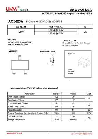
R UMW UMW AO3423A SOT-23-3L Plastic-Encapsulate MOSFETS P-Channel 20-V(D-S) MOSFET AO3423A V(BR)DSS RDS(on)MAX ID 120m @-4.5V -20 V -2A 150m @-2.5V FEATURE APPLICATION TrenchFET Power MOSFET Load Switch for Portable Devices ESD Protected 2.0KV DC/DC Converter MARKING Equivalent Circuit SOT 23 1. GATE 2. SOURCE 3. DRAIN Maximum ratings ( Ta=25 un
9.20. Size:282K umw-ic
ao3422a.pdf 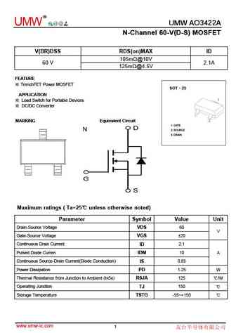
R UMW AO3422A UMW UMW AO3422A N-Channel 60-V(D-S) MOSFET V(BR)DSS RDS(on)MAX ID 105m @10V 60 V 2.1A 125m @4.5V FEATURE TrenchFET Power MOSFET SOT 23 APPLICATION Load Switch for Portable Devices t DC/DC Conver er MARKING Equivalent Circuit 1. GATE 2. SOURCE 3. DRAIN Maximum ratings ( Ta=25 unless otherwise noted) Parameter Symbol Value Unit Drain-Sou
9.21. Size:2456K anbon
ao3423b.pdf 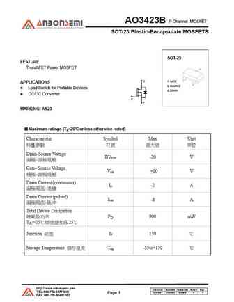
P-Channel MOSFET AO3423B SOT-23 Plastic-Encapsulate MOSFETS Dimensions In Millimeters Dimensions In Inches Symbol Min Max Min Max A 0.900 1.150 0.035 0.045 A1 0.000 0.100 0.000 0.004 A2 0.900 1.050 0.035 0.041 b 0.300 0.500 0.012 0.020 c 0.080 0.150 0.003 0.006 D 2.800 3.000 0.110 0.118 E 1.200 1.400 0.047 0.055 E1 2.250 2.550 0.089 0.100 e 0
9.22. Size:663K guangdong hottech
ao3420.pdf 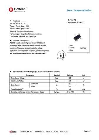
Plastic-Encapsulate Mosfets AO3420 Features N-Channel MOSFET VDS 20V, VGS 8V, ID 2.2A, RDS(ON) = 75m @VGS = 4.5V. RDS(ON) = 90m @VGS = 2.5V. Advanced trench process technology High-density cell design for ultra low on-resistance Compact and low profile SOT23 package General Description AO3420 is produced with high cell density DMOS trench technology, which is especi
9.23. Size:1502K cn shikues
ao3420.pdf 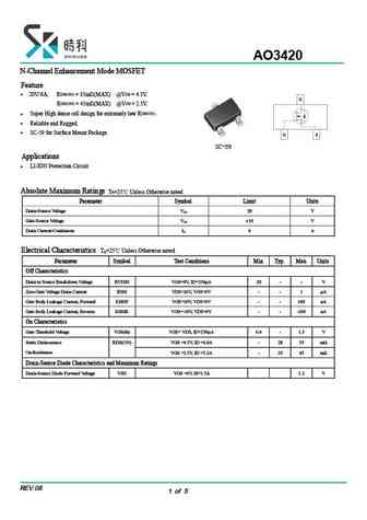
AO3420 N-Channel Enhancement Mode MOSFET Feature DS(ON) GS 20V/6A, R = 35m (MAX) @V = 4.5V. DS(ON) GS R = 45m (MAX) @V = 2.5V. SC-59 DS(ON) . Super High dense cell design for extremely low R Reliable and Rugged. SC-59 for Surface Mount Package. SC-59 A pplications LI-ION Protection Circuit Absolute Maximum Ratings A T =25 Unless Ot
9.24. Size:868K cn vbsemi
ao3423.pdf 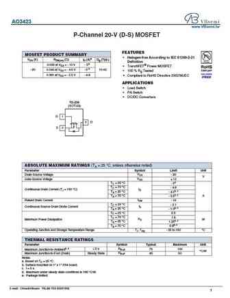
AO3423 www.VBsemi.tw P-Channel 20-V (D-S) MOSFET FEATURES MOSFET PRODUCT SUMMARY Halogen-free According to IEC 61249-2-21 VDS (V) RDS(on) ( )ID (A)a Qg (Typ.) Definition 0.035 at VGS = - 10 V - 5e TrenchFET Power MOSFET e - 20 0.043 at VGS = - 4.5 V - 5 10 nC 100 % Rg Tested 0.061 at VGS = - 2.5 V - 4.8 Compliant to RoHS Directive 2002/95/EC APPLICATIONS
9.25. Size:864K cn vbsemi
ao3422.pdf 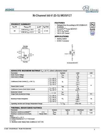
AO3422 www.VBsemi.tw N-Channel 60-V (D-S) MOSFET FEATURES PRODUCT SUMMARY Halogen-free According to IEC 61249-2-21 VDS (V) RDS(on) ( ) ID (A)a Qg (Typ.) Available TrenchFET Power MOSFET 0.085 at VGS = 10 V 4.0 60 2.1 nC 100 % Rg Tested 0.096 at VGS = 4.5 V 3.8 100 % UIS Tested APPLICATIONS Battery Switch DC/DC Converter D TO-236 (SOT23) G 1
9.26. Size:866K cn vbsemi
ao3421e.pdf 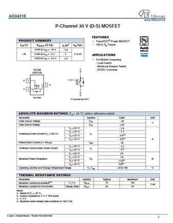
AO3421E www.VBsemi.tw P-Channel 30 V (D-S) MOSFET FEATURES PRODUCT SUMMARY TrenchFET Power MOSFET 100 % Rg Tested VDS (V) RDS(on) ( ) Typ. ID (A)a Qg (Typ.) 0.046 at VGS = - 10 V - 5.6 0.049 at VGS = - 6 V - 5 11.4 nC - 30 APPLICATIONS 0.054 at VGS = - 4.5 V -4.5 For Mobile Computing - Load Switch - Notebook Adaptor Switch S TO-236 - DC/DC Converter (SOT-23)
Другие MOSFET... AO3416
, AO3418
, AO3419
, AO3420
, AO3421
, AO3421E
, AO3422
, AO3423
, IRF9640
, AO3434
, AO3434A
, AO3435
, AO3438
, AO3442
, AO3460
, AO4202
, AO4240
.
History: DHS008N04P

