2SK2171 datasheet, аналоги, основные параметры
Наименование производителя: 2SK2171 📄📄
Тип транзистора: JFET
Полярность: N
Предельные значения
Pd ⓘ - Максимальная рассеиваемая мощность: 0.4 W
|Vds|ⓘ - Максимально допустимое напряжение сток-исток: 40 V
|Id| ⓘ - Максимально допустимый постоянный ток стока: 0.1 A
Tj ⓘ - Максимальная температура канала: 150 °C
Электрические характеристики
RDSonⓘ - Сопротивление сток-исток открытого транзистора: 30 Ohm
Тип корпуса: PCP
📄📄 Копировать
Аналог (замена) для 2SK2171
- подборⓘ MOSFET транзистора по параметрам
2SK2171 даташит
2sk2171.pdf
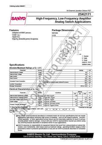
Ordering number ENN4871 N-Channel Junction Silicon FET 2SK2171 High-Frequency, Low-Frequency Amplifier Analog Switch Applications Features Package Dimensions Adoption of FBET process. unit mm Large yfs . 2125 Small Ciss. [2SK2171] High PD allowable power dissipation. 4.5 1.5 1.6 0.4 0.5 3 2 1 0.4 1.5 3.0 1 Source 2 Gate 0.75 3 Drain SANYO PCP
2sk2173.pdf
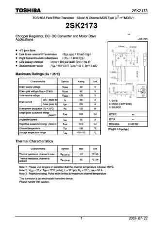
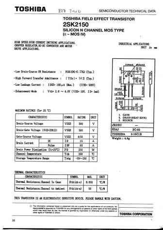
2SK2173 2 TOSHIBA Field Effect Transistor Silicon N Channel MOS Type (L - -MOSV) 2SK2173 Chopper Regulator, DC-DC Converter and Motor Drive Unit mm Applications 4 V gate drive Low drain-source ON resistance R = 13 m (typ.) DS (ON) High forward transfer admittance Y = 40 S (typ.) fs Low leakage current IDSS = 100 A (max) (V = 60 V) DS Enhancemen
2sk2170.pdf
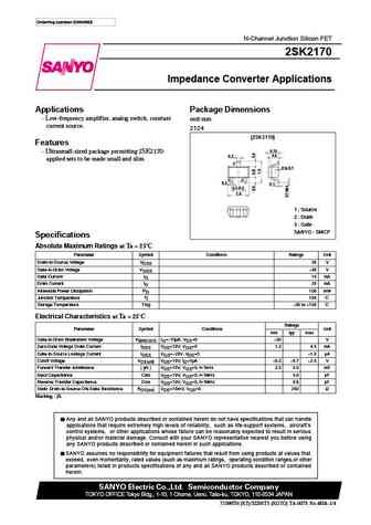
Ordering number ENN4858 N-Channel Junction Silicon FET 2SK2170 Impedance Converter Applications Applications Package Dimensions Low-frequency amplifier, analog switch, constant unit mm current source. 2124 [2SK2170] Features 0.75 Ultrasmall-sized package permitting 2SK2170- 0.3 0.6 applied sets to be made small and slim. 3 0 to 0.1 1 2 0.2 0.1 0.5 0.5 1.6 1 Sourc
2sk2157.pdf
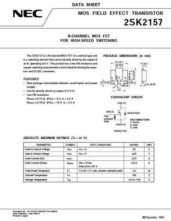
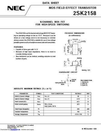
DATA SHEET MOS FIELD EFFECT TRANSISTOR 2SK2157 N-CHANNEL MOS FET FOR HIGH-SPEED SWITCHING The 2SK2157 is a N-channel MOS FET of a vertical type and PACKAGE DIMENSIONS (in mm) is a switching element that can be directly driven by the output of 5.7 0.1 an IC operating at 5 V. This product has a low ON resistance and 1.5 0.1 2.0 0.2 superb switching characteristics and is ideal fo
2sk2141.pdf
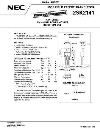
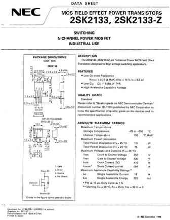
DATA SHEET MOS FIELD EFFECT TRANSISTOR 2SK2141 SWITCHING N-CHANNEL POWER MOS FET INDUSTRIAL USE DESCRIPTION PACKAGE DIMENSIONS The 2SK2141 is N-channel Power MOS Field Effect Transis- (in millimeters) tor designed for high voltage switching applications. 10.0 0.3 4.5 0.2 FEATURES 3.2 0.2 2.7 0.2 Low On-state Resistance RDS(on) = 1.1 MAX. (VGS = 10 V, ID = 3
2sk2140 2sk2140-z.pdf
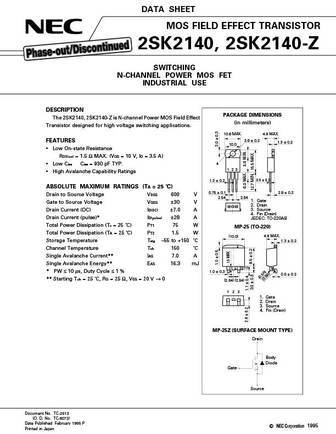
DATA SHEET MOS FIELD EFFECT TRANSISTOR 2SK2140, 2SK2140-Z SWITCHING N-CHANNEL POWER MOS FET INDUSTRIAL USE DESCRIPTION PACKAGE DIMENSIONS The 2SK2140, 2SK2140-Z is N-channel Power MOS Field Effect (in millimeters) Transistor designed for high voltage switching applications. 10.6 MAX. 4.8 MAX. 3.6 0.2 FEATURES 1.3 0.2 10.0 Low On-state Resistance RDS(on) = 1.5 MAX.

2sk2112.pdf
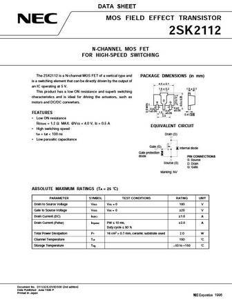
DATA SHEET MOS FIELD EFFECT TRANSISTOR 2SK2112 N-CHANNEL MOS FET FOR HIGH-SPEED SWITCHING The 2SK2112 is a N-channel MOS FET of a vertical type and PACKAGE DIMENSIONS (in mm) is a switching element that can be directly driven by the output of 4.5 0.1 an IC operating at 5 V. 1.6 0.2 1.5 0.1 This product has a low ON resistance and superb switching characteristics and is idea
2sk2110.pdf
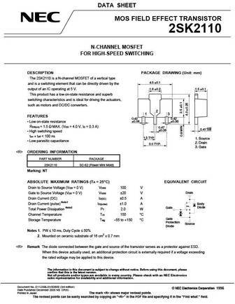
DATA SHEET MOS FIELD EFFECT TRANSISTOR 2SK2110 N-CHANNEL MOSFET FOR HIGH-SPEED SWITCHING DESCRIPTION PACKAGE DRAWING (Unit mm) The 2SK2110 is a N-channel MOSFET of a vertical type 4.5 0.1 and is a switching element that can be directly driven by the output of an IC operating at 5 V. 1.6 0.2 1.5 0.1 This product has a low on-state resistance and superb switching charact
2sk2137.pdf
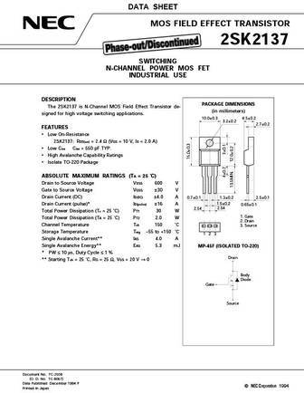
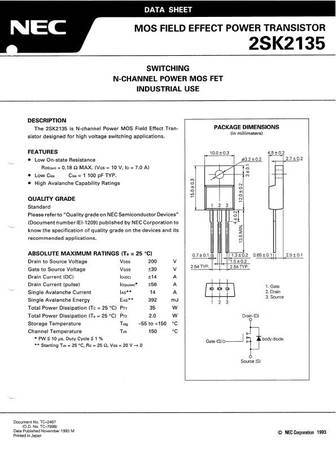
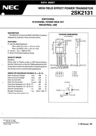
DATA SHEET MOS FIELD EFFECT TRANSISTOR 2SK2137 SWITCHING N-CHANNEL POWER MOS FET INDUSTRIAL USE DESCRIPTION PACKAGE DIMENSIONS The 2SK2137 is N-Channel MOS Field Effect Transistor de- (in millimeters) signed for high voltage switching applications. 10.0 0.3 4.5 0.2 3.2 0.2 2.7 0.2 FEATURES Low On-Resistance 2SK2137 RDS(on) = 2.4 (VGS = 10 V, ID = 2.0 A) Low Cis
2sk2138 2sk2138-z.pdf
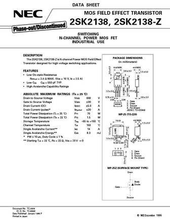
DATA SHEET MOS FIELD EFFECT TRANSISTOR 2SK2138, 2SK2138-Z SWITCHING N-CHANNEL POWER MOS FET INDUSTRIAL USE DESCRIPTION PACKAGE DIMENSIONS The 2SK2138, 2SK2138-Z is N-channel Power MOS Field Effect (in millimeters) Transistor designed for high voltage switching applications. 10.6 MAX. 4.8 MAX. 3.6 0.2 FEATURES 1.3 0.2 10.0 Low On-state Resistance RDS(on) = 2.4 MAX.
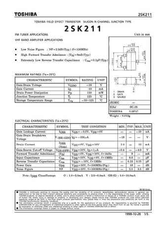
2sk210.pdf
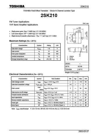
2SK210 TOSHIBA Field Effect Transistor Silicon N Channel Junction Type 2SK210 FM Tuner Applications Unit mm VHF Band Amplifier Applications High power gain GPS = 24dB (typ.) (f = 100 MHz) Low noise figure NF = 1.8dB (typ.) (f = 100 MHz) High forward transfer admittance Yfs = 7 mS (typ.) (f = 1 kHz) Maximum Ratings (Ta = 25 C) Characteristics Symbol Rating
2sk2145.pdf
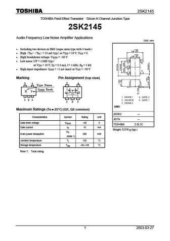
2SK2145 TOSHIBA Field Effect Transistor Silicon N Channel Junction Type 2SK2145 Audio Frequency Low Noise Amplifier Applications Unit mm Including two devices in SM5 (super mini type with 5 leads.) High Y Y = 15 mS (typ.) at V = 10 V, V = 0 fs fs DS GS High breakdown voltage V = -50 V GDS Low noise NF = 1.0dB (typ.) at V = 10 V, I = 0.5 mA, f = 1 k
2sk2199.pdf
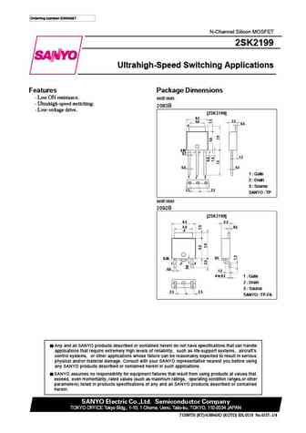
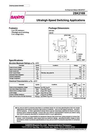
Ordering number ENN4557 N-Channel Silicon MOSFET 2SK2199 Ultrahigh-Speed Switching Applications Features Package Dimensions Low ON resistance. unit mm Ultrahigh-speed switching. 2083B Low-voltage drive. [2SK2199] 6.5 2.3 5.0 0.5 4 0.85 0.7 1.2 0.6 0.5 1 Gate 1 2 3 2 Drain 3 Source 2.3 2.3 SANYO TP unit mm 2092B [2SK2199] 6.5 2.3 5.0 0.5 4 0.5
2sk2160.pdf
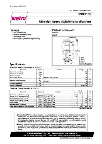
Ordering number ENN4600A N-Channel Silicon MOSFET 2SK2160 Ultrahigh-Speed Switching Applications Features Package Dimensions Low ON resistance. unit mm Ultrahigh-speed switching. 2063A Low-voltage drive. [2SK2160] Micaless package facilitating mounting. 4.5 10.0 2.8 3.2 2.4 1.6 1.2 0.7 0.75 1 2 3 1 Gate 2.55 2.55 2 Drain 3 Source 2.55 2.55 SANYO
2sk2151.pdf
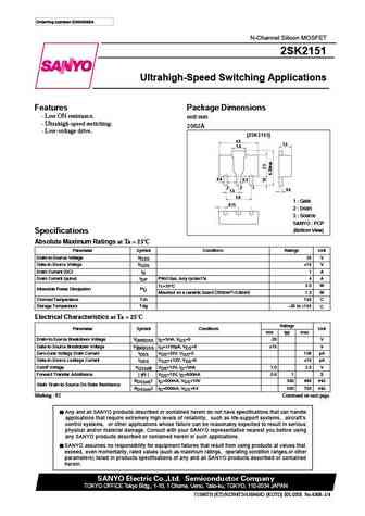
Ordering number ENN4568A N-Channel Silicon MOSFET 2SK2151 Ultrahigh-Speed Switching Applications Features Package Dimensions Low ON resistance. unit mm Ultrahigh-speed switching. 2062A Low-voltage drive. [2SK2151] 4.5 1.5 1.6 0.4 0.5 3 2 1 0.4 1.5 3.0 1 Gate 0.75 2 Drain 3 Source SANYO PCP (Bottom View) Specifications Absolute Maximum Ratings at Ta
2sk212.pdf
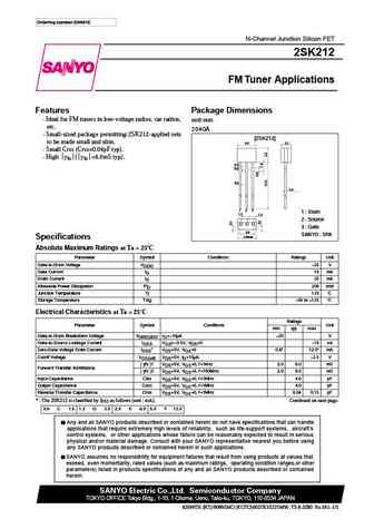
Ordering number EN661E N-Channel Junction Silicon FET 2SK212 FM Tuner Applications Features Package Dimensions Ideal for FM tuners in low-voltage radios, car radios, unit mm etc. 2040A Small-sized package permitting 2SK212-applied sets [2SK212] to be made small and slim. 2.2 4.0 Small Crss (Crss=0.04pF typ). High yfs ( yfs =6.0mS typ). 0.4 0.5 0.4
2sk2167.pdf
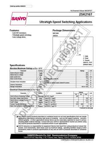
Ordering number ENN4631 N-Channel Silicon MOSFET 2SK2167 Ultrahigh-Speed Switching Applications Features Package Dimensions Low ON resistance. unit mm Ultrahigh-speed switching. 2062A Low-voltage drive. [2SK2167] 4.5 1.5 1.6 0.4 0.5 3 2 1 0.4 1.5 1 Gate 3.0 2 Drain 0.75 3 Source SANYO PCP (Bottom View) Specifications Absolute Maximum Ratings at Ta =
2sk2154.pdf
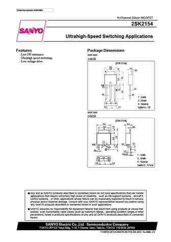
Ordering number ENN4689 N-Channel Silicon MOSFET 2SK2154 Ultrahigh-Speed Switching Applications Features Package Dimensions Low ON resistance. unit mm Ultrahigh-speed switching. 2083B Low-voltage drive. [2SK2154] 6.5 2.3 5.0 0.5 4 0.85 0.7 1.2 0.6 0.5 1 Gate 1 2 3 2 Drain 3 Source 2.3 2.3 SANYO TP unit mm 2092B [2SK2154] 6.5 2.3 5.0 0.5 4 0.5
2sk2152.pdf

Ordering number ENN4569A N-Channel Silicon MOSFET 2SK2152 Ultrahigh-Speed Switching Applications Features Package Dimensions Low ON resistance. unit mm Ultrahigh-speed switching. 2062A Low-voltage drive. [2SK2152] 4.5 1.5 1.6 0.4 0.5 3 2 1 0.4 1.5 3.0 1 Gate 0.75 2 Drain 3 Source SANYO PCP (Bottom View) Specifications Absolute Maximum Ratings at Ta
2sk2169.pdf
Ordering number ENN4556 N-Channel Silicon MOSFET 2SK2169 Ultrahigh-Speed Switching Applications Features Package Dimensions Low ON resistance. unit mm Ultrahigh-speed switching. 2087A Low-voltage drive. [2SK2169] 2.5 1.45 6.9 1.0 0.6 0.9 0.5 1 2 3 0.45 1 Source 2 Drain 3 Gate 2.54 2.54 SANYO NMP Specifications Absolute Maximum Ratings at Ta = 25 C P
2sk2108.pdf
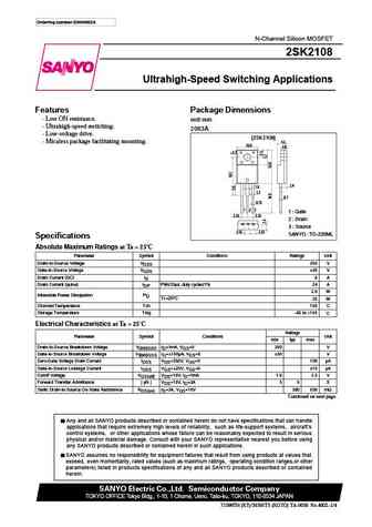
Ordering number ENN4602A N-Channel Silicon MOSFET 2SK2108 Ultrahigh-Speed Switching Applications Features Package Dimensions Low ON resistance. unit mm Ultrahigh-speed switching. 2063A Low-voltage drive. [2SK2108] Micaless package facilitating mounting. 4.5 10.0 2.8 3.2 2.4 1.6 1.2 0.7 0.75 1 2 3 1 Gate 2.55 2.55 2 Drain 3 Source 2.55 2.55 SANYO
2sk2161.pdf

Ordering number ENN4601A N-Channel Silicon MOSFET 2SK2161 Ultrahigh-Speed Switching Applications Features Package Dimensions Low ON resistance. unit mm Ultrahigh-speed switching. 2063A Low-voltage drive. [2SK2161] Micaless package facilitating mounting. 4.5 10.0 2.8 3.2 2.4 1.6 1.2 0.7 0.75 1 2 3 1 Gate 2.55 2.55 2 Drain 3 Source 2.55 2.55 SANYO
2sk2157c.pdf
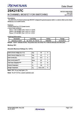
Preliminary Data Sheet 2SK2157C R07DS1264EJ0200 Rev.2.00 N-CHANNEL MOSFET FOR SWITCHING Jun 18, 2015 Description The 2SK2157C, N-channel vertical type MOSFET designed for general-purpose switch, is a device which can be driven directly by a 2.5 V power source. Features Directly driven by a 2.5 V power source. Low on-state resistance RDS(on)1 = 63 m MAX. (VGS = 4
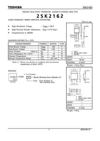
rej03g0903 2sk213 2sk214 2sk215 2sk216 a.pdf
To our customers, Old Company Name in Catalogs and Other Documents On April 1st, 2010, NEC Electronics Corporation merged with Renesas Technology Corporation, and Renesas Electronics Corporation took over all the business of both companies. Therefore, although the old company name remains in this document, it is a valid Renesas Electronics document. We appreciate your understanding.
2sk2109.pdf
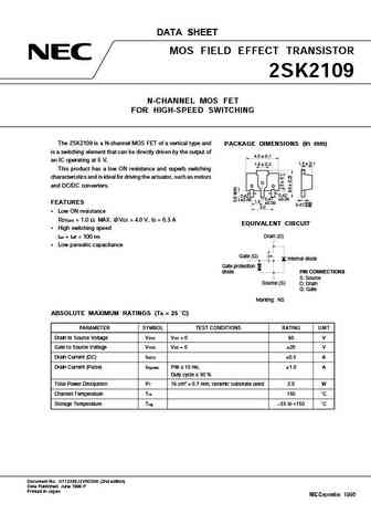
DATA SHEET MOS FIELD EFFECT TRANSISTOR 2SK2109 N-CHANNEL MOS FET FOR HIGH-SPEED SWITCHING The 2SK2109 is a N-channel MOS FET of a vertical type and PACKAGE DIMENSIONS (in mm) is a switching element that can be directly driven by the output of 4.5 0.1 an IC operating at 5 V. 1.5 0.1 1.6 0.2 This product has a low ON resistance and superb switching characteristics and is ide
2sk2159.pdf
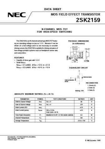
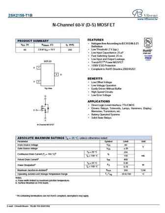
DATA SHEET MOS FIELD EFFECT TRANSISTOR 2SK2159 N-CHANNEL MOS FET FOR HIGH-SPEED SWITCHING The 2SK2159 is an N-channel vertical type MOS FET featur- PACKAGE DIMENSIONS ing an operating voltage as low as 1.5 V. Because it can be (in millimeters) driven on a low voltage and it is not necessary to consider 4.5 0.1 driving current, the 2SK2159 is suitable for driving actuators of 1.6
2sk2139.pdf
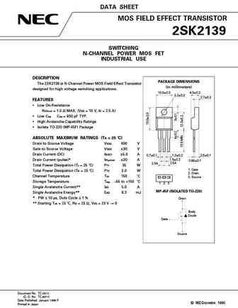
DATA SHEET MOS FIELD EFFECT TRANSISTOR 2SK2139 SWITCHING N-CHANNEL POWER MOS FET INDUSTRIAL USE DESCRIPTION PACKAGE DIMENSIONS The 2SK2139 is N-Channel Power MOS Field Effect Transistor (in millimeters) designed for high voltage switching applications. 10.0 0.3 4.5 0.2 3.2 0.2 2.7 0.2 FEATURES Low On-Resistance RDS(on) = 1.5 MAX. (VGS = 10 V, ID = 2.5 A) Low Cis

2sk2158.pdf
DATA SHEET MOS FIELD EFFECT TRANSISTOR 2SK2158 N-CHANNEL MOS FET FOR HIGH-SPEED SWITCHING The 2SK2158 is an N-channel vertical type MOS FET featur- PACKAGE DIMENSIONS ing an operating voltage as low as 1.5 V. Because it can be (in millimeters) driven on a low voltage and it is not necessary to consider 2.8 0.2 driving current, the 2SK2158 is suitable for use in low-voltage 1.5 0.
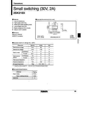
2sk2103.pdf
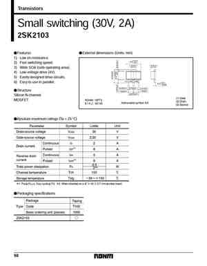
Transistors Small switching (30V, 2A) 2SK2103 FFeatures FExternal dimensions (Units mm) 1) Low on-resistance. 2) Fast switching speed. 3) Wide SOA (safe operating area). 4) Low-voltage drive (4V). 5) Easily designed drive circuits. 6) Easy to use in parallel. FStructure Silicon N-channel MOSFET FAbsolute maximum ratings (Ta = 25_C) FPackaging specifications 98 Transistors 2SK
2sk2128.pdf

Power F-MOS FETs 2SK2128 2SK2128 Silicon N-Channel Power F-MOS Unit mm Features Avalanche energy capability guaranteed EAS >15mJ 4.6 0.2 9.9 0.3 2.9 0.2 VGSS= 20V guaranteed 3.2 0.1 High-speed switching tf= 35ns No secondary breakdown 2.6 0.1 Applications 1.2 0.15 1.45 0.15 0.7 0.1 Non-contact relay 0.75 0.1 Solenoid drive 2.54 0.2 Motor drive
2sk2123.pdf

Power F-MOS FETs 2SK2123 2SK2123 Silicon N-Channel Power F-MOS Unit mm Features Avalanche energy capability guaranteed EAS > 100mJ 4.6 0.2 9.9 0.3 2.9 0.2 VGSS= 30V guaranteed 3.2 0.1 High-speed switching tf= 35ns No secondary breakdown 2.6 0.1 Applications 1.2 0.15 1.45 0.15 0.7 0.1 Non-contact relay 0.75 0.1 Solenoid drive 2.54 0.2 Motor driv
2sk2126.pdf

Power F-MOS FETs 2SK2126 2SK2126 Silicon N-Channel Power F-MOS Unit mm Features Avalanche energy capability guaranteed EAS > 100mJ 4.6 0.2 9.9 0.3 2.9 0.2 VGSS= 30V guaranteed 3.2 0.1 High-speed switching tf= 40ns No secondary breakdown 2.6 0.1 Applications 1.2 0.15 1.45 0.15 0.7 0.1 Non-contact relay 0.75 0.1 Solenoid drive 2.54 0.2 Motor driv
2sk2127.pdf

Power F-MOS FETs 2SK2127 2SK2127 Silicon N-Channel Power F-MOS Unit mm Features Avalanche energy capability guaranteed EAS > 130mJ 4.6 0.2 9.9 0.3 2.9 0.2 VGSS= 30V guaranteed 3.2 0.1 High-speed switching tf= 60ns No secondary breakdown 2.6 0.1 Applications 1.2 0.15 1.45 0.15 0.7 0.1 Non-contact relay 0.75 0.1 Solenoid drive 2.54 0.2 Motor driv
2sk2122.pdf
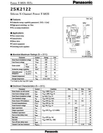
Power F-MOS FETs 2SK2122 2SK2122 Silicon N-Channel Power F-MOS Unit mm Features Avalanche energy capability guaranteed EAS > 3.2mJ 4.6 0.2 9.9 0.3 2.9 0.2 High-speed switching tf= 50ns 3.2 0.1 No secondary breakdown Applications 2.6 0.1 Non-contact relay 1.2 0.15 1.45 0.15 0.7 0.1 Solenoid drive 0.75 0.1 Motor drive 2.54 0.2 Control equipment 5
2sk2129.pdf

Power F-MOS FETs 2SK2129 2SK2129 Silicon N-Channel Power F-MOS Unit mm Features Avalanche energy capability guaranteed EAS > 20mJ 4.6 0.2 9.9 0.3 2.9 0.2 VGSS= 30V guaranteed 3.2 0.1 High-speed switching tf= 50ns No secondary breakdown 2.6 0.1 Applications 1.2 0.15 1.45 0.15 0.7 0.1 Non-contact relay 0.75 0.1 Solenoid drive 2.54 0.2 Motor drive
2sk2124.pdf

Power F-MOS FETs 2SK2124 2SK2124 Silicon N-Channel Power F-MOS Unit mm Features Avalanche energy capability guaranteed EAS > 130mJ 4.6 0.2 9.9 0.3 2.9 0.2 VGSS= 30V guaranteed 3.2 0.1 High-speed switching tf= 60ns No secondary breakdown 2.6 0.1 Applications 1.2 0.15 1.45 0.15 0.7 0.1 Non-contact relay 0.75 0.1 Solenoid drive 2.54 0.2 Motor driv
2sk2130.pdf

Power F-MOS FETs 2SK2130 2SK2130 Silicon N-Channel Power F-MOS Unit mm Features Avalanche energy capability guaranteed EAS > 15mJ 4.6 0.2 9.9 0.3 2.9 0.2 VGSS= 30V guaranteed 3.2 0.1 High-speed switching tf= 45ns No secondary breakdown 2.6 0.1 Applications 1.2 0.15 1.45 0.15 0.7 0.1 Non-contact relay 0.75 0.1 Solenoid drive 2.54 0.2 Motor drive
2sk2125.pdf

Power F-MOS FETs 2SK2125 2SK2125 Silicon N-Channel Power F-MOS Unit mm Features Avalanche energy capability guaranteed EAS > 15.6mJ 4.6 0.2 9.9 0.3 2.9 0.2 VGSS= 30V guaranteed 3.2 0.1 High-speed switching tf= 35ns No secondary breakdown 2.6 0.1 Applications 1.2 0.15 1.45 0.15 0.7 0.1 Non-contact relay 0.75 0.1 Solenoid drive 2.54 0.2 Motor dri
2sk2148-01.pdf
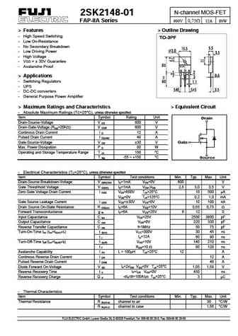
N-channel MOS-FET 2SK2148-01 FAP-IIA Series 600V 0,75 12A 80W > Features > Outline Drawing - High Speed Switching - Low On-Resistance - No Secondary Breakdown - Low Driving Power - High Voltage - VGS = 30V Guarantee - Avalanche Proof > Applications - Switching Regulators - UPS - DC-DC converters - General Purpose Power Amplifier > Maximum Ratings and Characteristics > Equi
2sk2101 01mr.pdf
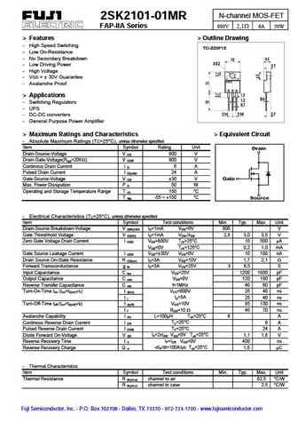
N-channel MOS-FET 2SK2101-01MR FAP-IIA Series 800V 2,1 6A 50W > Features > Outline Drawing - High Speed Switching - Low On-Resistance - No Secondary Breakdown - Low Driving Power - High Voltage - VGS = 30V Guarantee - Avalanche Proof > Applications - Switching Regulators - UPS - DC-DC converters - General Purpose Power Amplifier > Maximum Ratings and Characteristics > Equ
2sk2114 2sk2115.pdf

2SK2114, 2SK2115 Silicon N-Channel MOS FET Application High speed power switching Features Low on-resistance High speed switching Low drive current No secondary breakdown Suitable for Switching regulator Outline TO-220CFM 1 D 2 3 1. Gate G 2. Drain 3. Source S 2SK2114, 2SK2115 Absolute Maximum Ratings (Ta = 25 C) Item Symbol Ratings Unit Drain to so
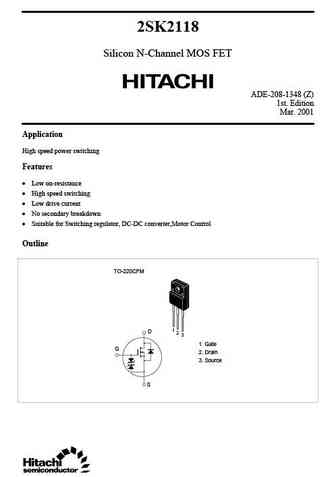
2sk2118.pdf
2SK2118 Silicon N-Channel MOS FET ADE-208-1348 (Z) 1st. Edition Mar. 2001 Application High speed power switching Features Low on-resistance High speed switching Low drive current No secondary breakdown Suitable for Switching regulator, DC-DC converter,Motor Control Outline TO-220CFM 1 D 2 3 1. Gate G 2. Drain 3. Source S 2SK2118 Absolute Maximum Rat
2sk213 2sk214 2sk215 2sk216.pdf
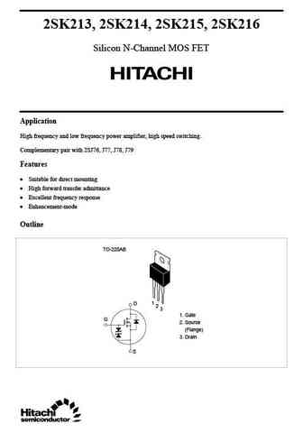
2SK213, 2SK214, 2SK215, 2SK216 Silicon N-Channel MOS FET Application High frequency and low frequency power amplifier, high speed switching. Complementary pair with 2SJ76, J77, J78, J79 Features Suitable for direct mounting High forward transfer admittance Excellent frequency response Enhancement-mode Outline TO-220AB 1 D 2 3 1. Gate G 2. Source (Flange) 3. D
2sk2116 2sk2117.pdf
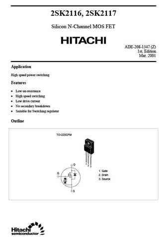
2SK2116, 2SK2117 Silicon N-Channel MOS FET ADE-208-1347 (Z) 1st. Edition Mar. 2001 Application High speed power switching Features Low on-resistance High speed switching Low drive current No secondary breakdown Suitable for Switching regulator Outline TO-220CFM 1 D 2 3 1. Gate G 2. Drain 3. Source S 2SK2116, 2SK2117 Ordering Information Type No. VD
2sk1871 2sk2153 2sk2164 2sk2321 2sk2432 2sk2435 2sk2436 2sk2438 2sk2439 2sk2626 2sk2634 2sk2635 2sk2636 2sk2637 2sk2773.pdf
2sk2190 fp10w50vx2.pdf

SHINDENGEN VX-2 Series Power MOSFET N-Channel Enhancement type OUTLINE DIMENSIONS 2SK2190 Case E-pack Case ITO-3P (Unit mm) (FP10W50VX2) 500V 10A FEATURES Input capacitance (Ciss) is small. Especially, input capacitance at 0 biass is small. The static Rds(on) is small. The switching time is fast. APPLICATION Switching power supply of AC 100V input High vo
2sk2197 fp20w50vx2.pdf

SHINDENGEN VX-2 Series Power MOSFET N-Channel Enhancement type OUTLINE DIMENSIONS 2SK2197 Case E-pack Case ITO-3P (Unit mm) (FP20W50VX2) 500V 20A FEATURES Input capacitance (Ciss) is small. Especially, input capacitance at 0 biass is small. The static Rds(on) is small. The switching time is fast. APPLICATION Switching power supply of AC 100V input High vo
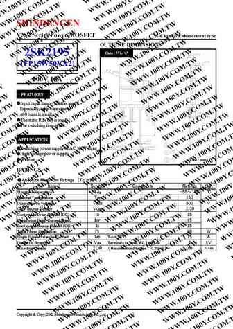
2sk2193.pdf
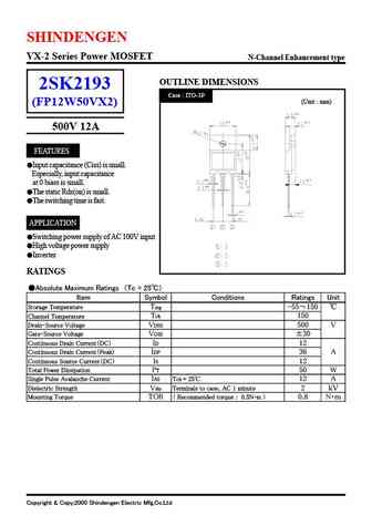
SHINDENGEN VX-2 Series Power MOSFET N-Channel Enhancement type OUTLINE DIMENSIONS 2SK2193 Case E-pack Case ITO-3P (Unit mm) (FP12W50VX2) 500V 12A FEATURES Input capacitance (Ciss) is small. Especially, input capacitance at 0 biass is small. The static Rds(on) is small. The switching time is fast. APPLICATION Switching power supply of AC 100V input High vo
2sk2182.pdf
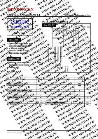
SHINDENGEN VX-2 Series Power MOSFET N-Channel Enhancement type OUTLINE DIMENSIONS 2SK2182 Case E-pack Case FTO-220 (Unit mm) (F3F50VX2) 500V 3A FEATURES Input capacitance (Ciss) is small. Especially, input capacitance at 0 biass is small. The static Rds(on) is small. The switching time is fast. APPLICATION Switching power supply of AC 100V input High
2sk2192 f12w50vx2.pdf

SHINDENGEN VX-2 Series Power MOSFET N-Channel Enhancement type OUTLINE DIMENSIONS 2SK2192 Case E-pack Case MTO-3P (Unit mm) (F12W50VX2) 500V 12A FEATURES Input capacitance (Ciss) is small. Especially, input capacitance at 0 biass is small. The static Rds(on) is small. The switching time is fast. APPLICATION Switching power supply of AC 100V input High vol
2sk2191.pdf
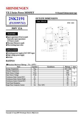
SHINDENGEN VX-2 Series Power MOSFET N-Channel Enhancement type OUTLINE DIMENSIONS 2SK2191 Case E-pack Case STO-220 (Unit mm) (F12S50VX2) 500V 12A FEATURES Input capacitance (Ciss) is small. Especially, input capacitance at 0 biass is small. The static Rds(on) is small. The switching time is fast. APPLICATION Switching power supply of AC 100V input High vo
2sk2180.pdf
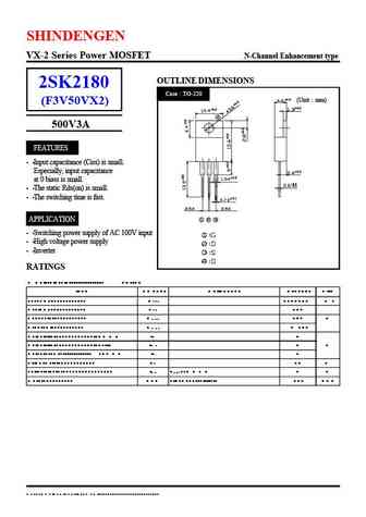
SHINDENGEN VX-2 Series Power MOSFET N-Channel Enhancement type OUTLINE DIMENSIONS 2SK2180 Case E-pack Case TO-220 (Unit mm) (F3V50VX2) 500V3A FEATURES Input capacitance (Ciss) is small. Especially, input capacitance at 0 biass is small. The static Rds(on) is small. The switching time is fast. APPLICATION Switching power supply of AC 100V input High v
2sk2186.pdf

SHINDENGEN VX-2 Series Power MOSFET N-Channel Enhancement type OUTLINE DIMENSIONS 2SK2186 Case E-pack Case TO-220 (Unit mm) (F10V50VX2) 500V 10A FEATURES Input capacitance (Ciss) is small. Especially, input capacitance at 0 biass is small. The static Rds(on) is small. The switching time is fast. APPLICATION Switching power supply of AC 100V input Hig
2sk2188 f10f50vx2.pdf
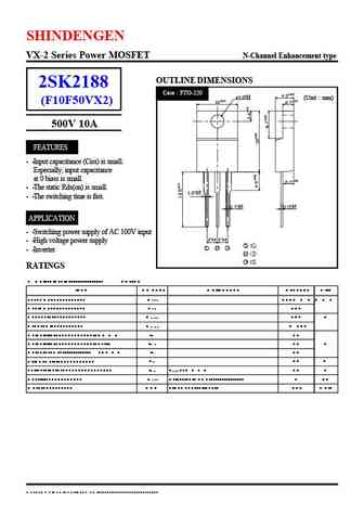
SHINDENGEN VX-2 Series Power MOSFET N-Channel Enhancement type OUTLINE DIMENSIONS 2SK2188 Case E-pack Case FTO-220 (Unit mm) (F10F50VX2) 500V 10A FEATURES Input capacitance (Ciss) is small. Especially, input capacitance at 0 biass is small. The static Rds(on) is small. The switching time is fast. APPLICATION Switching power supply of AC 100V input Hi
2sk2196.pdf
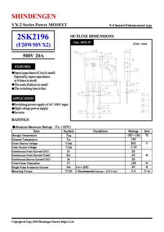
SHINDENGEN VX-2 Series Power MOSFET N-Channel Enhancement type OUTLINE DIMENSIONS 2SK2196 Case MTO-3P (Unit mm) (F20W50VX2) 500V 20A FEATURES Input capacitance (Ciss) is small. Especially, input capacitance at 0 biass is small. The static Rds(on) is small. The switching time is fast. APPLICATION Switching power supply of AC 100V input High voltage power supply Inverter R
2sk2189.pdf

SHINDENGEN VX-2 Series Power MOSFET N-Channel Enhancement type OUTLINE DIMENSIONS 2SK2189 Case E-pack Case MTO-3P (Unit mm) (F10W50VX2) 500V 10A FEATURES Input capacitance (Ciss) is small. Especially, input capacitance at 0 biass is small. The static Rds(on) is small. The switching time is fast. APPLICATION Switching power supply of AC 100V input High vol
2sk2185.pdf
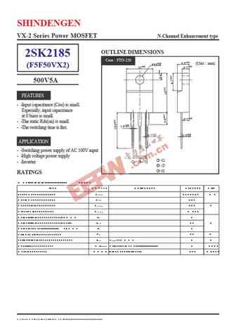
SHINDENGEN VX-2 Series Power MOSFET N-Channel Enhancement type OUTLINE DIMENSIONS 2SK2185 Case E-pack Case FTO-220 (Unit mm) (F5F50VX2) 500V5A FEATURES Input capacitance (Ciss) is small. Especially, input capacitance at 0 biass is small. The static Rds(on) is small. The switching time is fast. APPLICATION Switching power supply of AC 100V input High
2sk2195.pdf
SHINDENGEN VX-2 Series Power MOSFET N-Channel Enhancement type OUTLINE DIMENSIONS Case ITO-3P 2SK2195 (FP15W50VX2) 500V 15A FEATURES Input capacitance (Ciss) is small. Especially, input capacitance at 0 biass is small. The static Rds(on) is small. The switching time is fast. APPLICATION Switching power supply of AC 100V input High voltage power supply Inverter (Unit mm) R
2sk2194 f15w50vx2.pdf
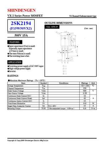
SHINDENGEN VX-2 Series Power MOSFET N-Channel Enhancement type OUTLINE DIMENSIONS 2SK2194 Case E-pack Case MTO-3P (Unit mm) (F15W50VX2) 500V 15A FEATURES Input capacitance (Ciss) is small. Especially, input capacitance at 0 biass is small. The static Rds(on) is small. The switching time is fast. APPLICATION Switching power supply of AC 100V input High vol
2sk2109.pdf
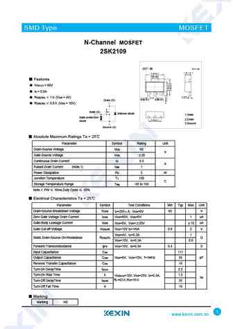
SMD Type MOSFET N-Channel MOSFET 2SK2109 1.70 0.1 Features VDS (V) = 60V ID = 0.5A RDS(ON) 1 (VGS = 4V) 0.42 0.1 0.46 0.1 Drain (D) RDS(ON) 0.8 (VGS = 10V) Gate (G) Internal diode 1.Gate Gate protection 2.Drain diode 3.Source Source (S) Absolute Maximum Ratings Ta = 25 Parameter Symbol Rating Unit Drain-Source Voltage VDS 60 V
2sk2159.pdf
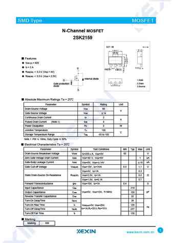
SMD Type MOSFET N-Channel MOSFET 2SK2159 1.70 0.1 Features VDS (V) = 60V ID = 2 A D 0.42 0.1 0.46 0.1 RDS(ON) 0.3 (VGS = 4V) RDS(ON) 0.5 (VGS = 2.5V) Internal diode 1.Gate G 2.Drain Gate protection diode 3.Source S Absolute Maximum Ratings Ta = 25 Parameter Symbol Rating Unit Drain-Source Voltage VDS 60 V Gate-Source Voltage
2sk2112.pdf

SMD Type MOSFET N-Channel MOSFET 2SK2112 1.70 0.1 Features VDS (V) = 100V ID = 1 A 0.42 0.1 0.46 0.1 RDS(ON) 0.8 (VGS = 10V) Drain (D) RDS(ON) 1.2 (VGS = 4V) 1.Gate 2.Drain Gate (G) Internal diode 3.Source Gate protection diode Source (S) Absolute Maximum Ratings Ta = 25 Parameter Symbol Rating Unit Drain-Source Voltage VDS 100
2sk2110.pdf
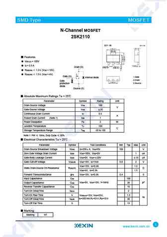
SMD Type MOSFET N-Channel MOSFET 2SK2110 1.70 0.1 Features VDS (V) = 100V ID = 0.5 A Drain (D) 0.42 0.1 0.46 0.1 RDS(ON) 1.2 (VGS = 10V) RDS(ON) 1.5 (VGS = 4V) Gate (G) 1.Gate Internal diode 2.Drain Gate 3.Source protection diode Source (S) Absolute Maximum Ratings Ta = 25 Parameter Symbol Rating Unit Drain-Source Voltage VDS 10
2sk2111.pdf
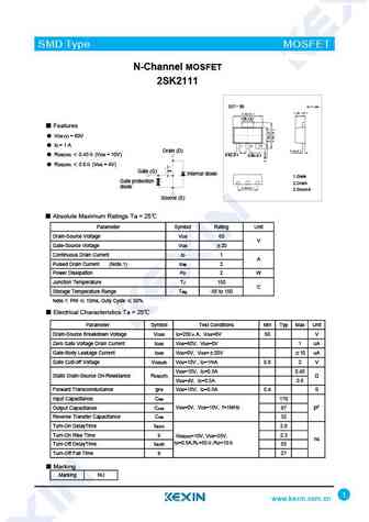
SMD Type MOSFET N-Channel MOSFET 2SK2111 1.70 0.1 Features VDS (V) = 60V ID = 1 A Drain (D) RDS(ON) 0.45 (VGS = 10V) 0.42 0.1 0.46 0.1 RDS(ON) 0.6 (VGS = 4V) Gate (G) Internal diode 1.Gate Gate protection 2.Drain diode 3.Source Source (S) Absolute Maximum Ratings Ta = 25 Parameter Symbol Rating Unit Drain-Source Voltage VDS 60 V
2sk2159.pdf
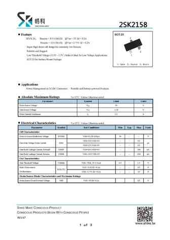
2SK2159 www.VBsemi.tw N-Channel 60-V (D-S) MOSFET FEATURES PRODUCT SUMMARY Halogen-free VDS (V) RDS(on) ( ) ID (A)a Qg (Typ.) TrenchFET Power MOSFET 0.076 at VGS = 4.5 V 7.1 RoHS 29 nC COMPLIANT 60 APPLICATIONS 0.088 at VGS = 10 V 6.7 Load Switches for Portable Devices D D G S G D S N-Channel MOSFET ABSOLUTE MAXIMUM RATINGS TA = 25 C, unless otherwise no
2sk2158-t1b.pdf
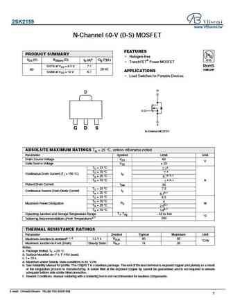
2SK2158-T1B www.VBsemi.tw N-Channel 60-V (D-S) MOSFET FEATURES PRODUCT SUMMARY Halogen-free According to IEC 61249-2-21 VDS (V) RDS(on) ( )ID (mA) Definition 2.8 at VGS = 10 V 60 250 Low Threshold 2 V (typ.) Low Input Capacitance 25 pF Fast Switching Speed 25 ns Low Input and Output Leakage SOT-23 TrenchFET Power MOSFET 1200V ESD Protection G
2sk2116.pdf
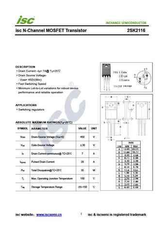
isc N-Channel MOSFET Transistor 2SK2116 DESCRIPTION Drain Current I = 7A@ T =25 D C Drain Source Voltage- V = 450V(Min) DSS Fast Switching Speed Minimum Lot-to-Lot variations for robust device performance and reliable operation APPLICATIONS Switching regulators ABSOLUTE MAXIMUM RATINGS(T =25 ) a SYMBOL ARAMETER VALUE UNIT V Drain-Source Voltage (V =0) 450 V D
2sk2188.pdf
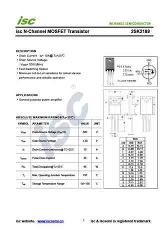
isc N-Channel MOSFET Transistor 2SK2188 DESCRIPTION Drain Current I = 10A@ T =25 D C Drain Source Voltage- V = 500V(Min) DSS Fast Switching Speed Minimum Lot-to-Lot variations for robust device performance and reliable operation APPLICATIONS General purpose power amplifier ABSOLUTE MAXIMUM RATINGS(T =25 ) a SYMBOL ARAMETER VALUE UNIT V Drain-Source Voltage (V =0)
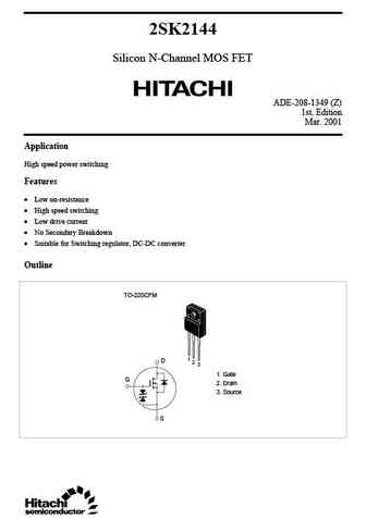
2sk2144.pdf
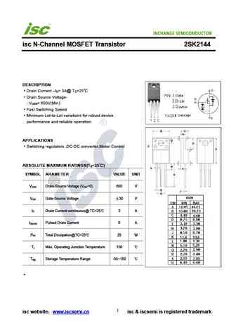
isc N-Channel MOSFET Transistor 2SK2144 DESCRIPTION Drain Current I = 3A@ T =25 D C Drain Source Voltage- V = 600V(Min) DSS Fast Switching Speed Minimum Lot-to-Lot variations for robust device performance and reliable operation APPLICATIONS Switching regulators ,DC-DC converter,Motor Control ABSOLUTE MAXIMUM RATINGS(T =25 ) a SYMBOL ARAMETER VALUE UNIT V Drain
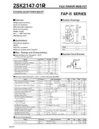
2sk2147-01.pdf
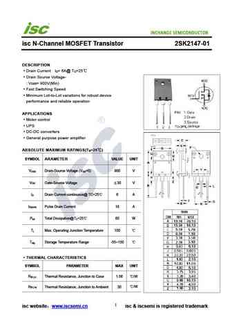
isc N-Channel MOSFET Transistor 2SK2147-01 DESCRIPTION Drain Current I = 6A@ T =25 D C Drain Source Voltage- V = 900V(Min) DSS Fast Switching Speed Minimum Lot-to-Lot variations for robust device performance and reliable operation APPLICATIONS Motor control UPS DC-DC converters General purpose power amplifier ABSOLUTE MAXIMUM RATINGS(T =25 ) a SYMBOL ARAM
2sk2149.pdf
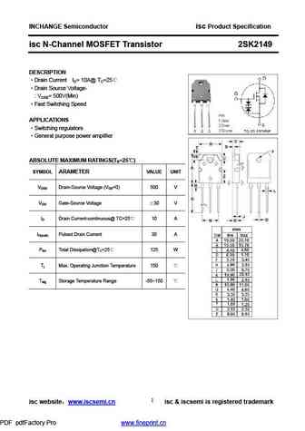
INCHANGE Semiconductor isc Product Specification isc N-Channel MOSFET Transistor 2SK2149 DESCRIPTION Drain Current ID= 10A@ TC=25 Drain Source Voltage- VDSS= 500V(Min) Fast Switching Speed APPLICATIONS Switching regulators General purpose power amplifier ABSOLUTE MAXIMUM RATINGS(Ta=25 ) SYMBOL VALUE UNIT ARAMETER VDSS Drain-Source Voltage (VGS=0) 500
2sk2118.pdf

isc N-Channel MOSFET Transistor 2SK2118 DESCRIPTION Drain Current I = 5A@ T =25 D C Drain Source Voltage- V = 600V(Min) DSS Fast Switching Speed Minimum Lot-to-Lot variations for robust device performance and reliable operation APPLICATIONS Switching regulators ,DC-DC converter,Motor Control ABSOLUTE MAXIMUM RATINGS(T =25 ) a SYMBOL ARAMETER VALUE UNIT V Drain
2sk2182.pdf
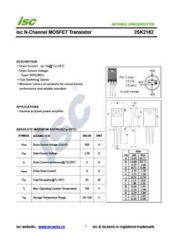
isc N-Channel MOSFET Transistor 2SK2182 DESCRIPTION Drain Current I = 3A@ T =25 D C Drain Source Voltage- V = 500V(Min) DSS Fast Switching Speed Minimum Lot-to-Lot variations for robust device performance and reliable operation APPLICATIONS General purpose power amplifier ABSOLUTE MAXIMUM RATINGS(T =25 ) a SYMBOL ARAMETER VALUE UNIT V Drain-Source Voltage (V =0)
2sk2108.pdf
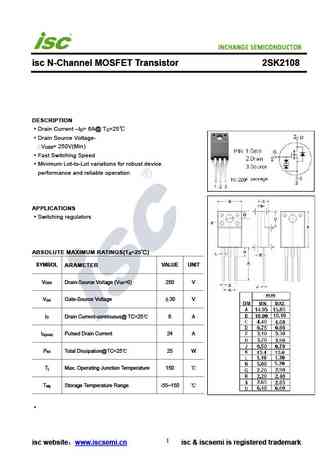
isc N-Channel MOSFET Transistor 2SK2108 DESCRIPTION Drain Current I = 6A@ T =25 D C Drain Source Voltage- V = 250V(Min) DSS Fast Switching Speed Minimum Lot-to-Lot variations for robust device performance and reliable operation APPLICATIONS Switching regulators ABSOLUTE MAXIMUM RATINGS(T =25 ) a SYMBOL ARAMETER VALUE UNIT V Drain-Source Voltage (V =0) 250 V D
2sk2146.pdf
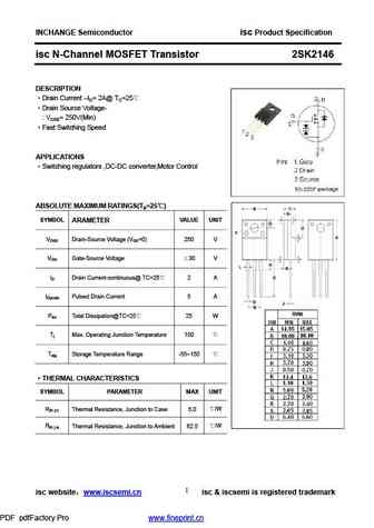
INCHANGE Semiconductor isc Product Specification isc N-Channel MOSFET Transistor 2SK2146 DESCRIPTION Drain Current ID= 2A@ TC=25 Drain Source Voltage- VDSS= 250V(Min) Fast Switching Speed APPLICATIONS Switching regulators ,DC-DC converter,Motor Control ABSOLUTE MAXIMUM RATINGS(Ta=25 ) SYMBOL VALUE UNIT ARAMETER VDSS Drain-Source Voltage (VGS=0) 250 V
2sk2148-01.pdf
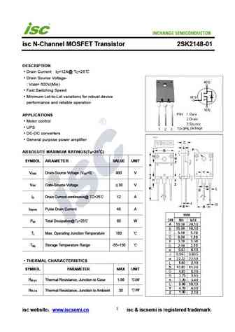
isc N-Channel MOSFET Transistor 2SK2148-01 DESCRIPTION Drain Current I =12A@ T =25 D C Drain Source Voltage- V = 600V(Min) DSS Fast Switching Speed Minimum Lot-to-Lot variations for robust device performance and reliable operation APPLICATIONS Motor control UPS DC-DC converters General purpose power amplifier ABSOLUTE MAXIMUM RATINGS(T =25 ) a SYMBOL ARAM
2sk2180.pdf
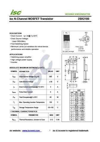
isc N-Channel MOSFET Transistor 2SK2180 DESCRIPTION Drain Current I = 3A@ T =25 D C Drain Source Voltage- V = 500V(Min) DSS Fast Switching Speed Minimum Lot-to-Lot variations for robust device performance and reliable operation APPLICATIONS Switching power amplifier High voltage power supply Inverter ABSOLUTE MAXIMUM RATINGS(T =25 ) a SYMBOL ARAMETER VALUE U
2sk2114.pdf
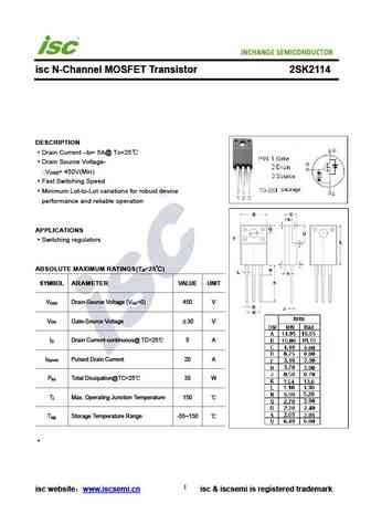
isc N-Channel MOSFET Transistor 2SK2114 DESCRIPTION Drain Current I = 5A@ T =25 D C Drain Source Voltage- V = 450V(Min) DSS Fast Switching Speed Minimum Lot-to-Lot variations for robust device performance and reliable operation APPLICATIONS Switching regulators ABSOLUTE MAXIMUM RATINGS(T =25 ) a SYMBOL ARAMETER VALUE UNIT V Drain-Source Voltage (V =0) 450 V D
2sk2150.pdf
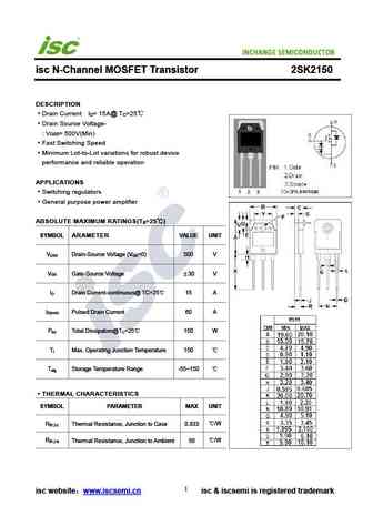
isc N-Channel MOSFET Transistor 2SK2150 DESCRIPTION Drain Current I = 15A@ T =25 D C Drain Source Voltage- V = 500V(Min) DSS Fast Switching Speed Minimum Lot-to-Lot variations for robust device performance and reliable operation APPLICATIONS Switching regulators General purpose power amplifier ABSOLUTE MAXIMUM RATINGS(T =25 ) a SYMBOL ARAMETER VALUE UNIT V Dra
2sk2183.pdf
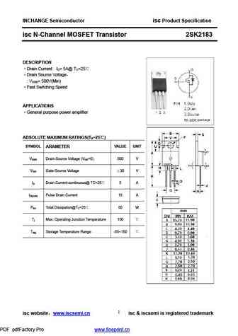
INCHANGE Semiconductor isc Product Specification isc N-Channel MOSFET Transistor 2SK2183 DESCRIPTION Drain Current ID= 5A@ TC=25 Drain Source Voltage- VDSS= 500V(Min) Fast Switching Speed APPLICATIONS General purpose power amplifier ABSOLUTE MAXIMUM RATINGS(Ta=25 ) SYMBOL VALUE UNIT ARAMETER VDSS Drain-Source Voltage (VGS=0) 500 V VGS Gate-Source Voltag
2sk2186.pdf
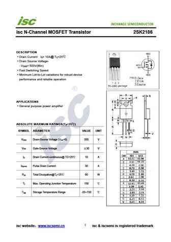
isc N-Channel MOSFET Transistor 2SK2186 DESCRIPTION Drain Current I = 10A@ T =25 D C Drain Source Voltage- V = 500V(Min) DSS Fast Switching Speed Minimum Lot-to-Lot variations for robust device performance and reliable operation APPLICATIONS General purpose power amplifier ABSOLUTE MAXIMUM RATINGS(T =25 ) a SYMBOL ARAMETER VALUE UNIT V Drain-Source Voltage (V =0)
2sk2185.pdf
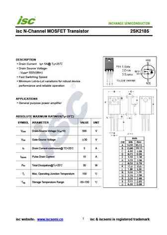
isc N-Channel MOSFET Transistor 2SK2185 DESCRIPTION Drain Current I = 5A@ T =25 D C Drain Source Voltage- V = 500V(Min) DSS Fast Switching Speed Minimum Lot-to-Lot variations for robust device performance and reliable operation APPLICATIONS General purpose power amplifier ABSOLUTE MAXIMUM RATINGS(T =25 ) a SYMBOL ARAMETER VALUE UNIT V Drain-Source Voltage (V =0)
2sk2117.pdf
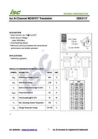
isc N-Channel MOSFET Transistor 2SK2117 DESCRIPTION Drain Current I = 7A@ T =25 D C Drain Source Voltage- V = 500V(Min) DSS Fast Switching Speed Minimum Lot-to-Lot variations for robust device performance and reliable operation APPLICATIONS Switching regulators ABSOLUTE MAXIMUM RATINGS(T =25 ) a SYMBOL ARAMETER VALUE UNIT V Drain-Source Voltage (V =0) 500 V D
2sk2115.pdf
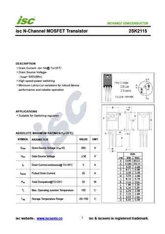
isc N-Channel MOSFET Transistor 2SK2115 DESCRIPTION Drain Current I = 5A@ T =25 D C Drain Source Voltage- V = 500V(Min) DSS High speed power switching Minimum Lot-to-Lot variations for robust device performance and reliable operation APPLICATIONS Suitable for Switching regulator ABSOLUTE MAXIMUM RATINGS(T =25 ) a SYMBOL ARAMETER VALUE UNIT V Drain-Source Volta
2sk2180-01.pdf
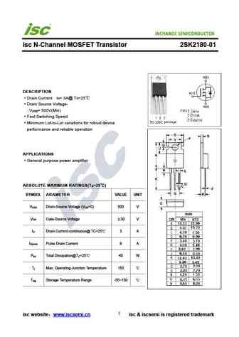
isc N-Channel MOSFET Transistor 2SK2180-01 DESCRIPTION Drain Current I = 3A@ T =25 D C Drain Source Voltage- V = 500V(Min) DSS Fast Switching Speed Minimum Lot-to-Lot variations for robust device performance and reliable operation APPLICATIONS General purpose power amplifier ABSOLUTE MAXIMUM RATINGS(T =25 ) a SYMBOL ARAMETER VALUE UNIT V Drain-Source Voltage (V =
Другие IGBT... FS10UM-9, FS10VS-9, FS10KM-9, FS10SM-9, 2SK3599-01MR, 2SK1506, 2SK3538, 2SK3699-01MR, TK10A60D, 2N5640, FTP08N50, FTA08N50, STP16NE06, STP16NE06FP, FTX30P35G, FTZ15N35G, FTZ20N01G5
Параметры MOSFET. Взаимосвязь и компромиссы
🌐 : EN ES РУ

Список транзисторов
Обновления
MOSFET: CB3139KTB | CB2301DW | BC8205 | BC3415 | BC3407 | BC3401 | BC3400 | BC2301 | BC1012W | BC1012T | BC1012 | 2SK3019WT | 2SK3019W | 2SK3018WT | CS95118 | CS85105A
Popular searches
fb42n20d | irfb3306 equivalent | irfp460 характеристики | k2837 datasheet | k389 transistor | mje15032g equivalent | nsd134 | 60r190p datasheet