SSF3616. Аналоги и основные параметры
Наименование производителя: SSF3616
Тип транзистора: MOSFET
Полярность: N
Предельные значения
Pd ⓘ - Максимальная рассеиваемая мощность: 2.5 W
|Vds|ⓘ - Максимально допустимое напряжение сток-исток: 30 V
|Vgs|ⓘ - Максимально допустимое напряжение затвор-исток: 25 V
|Id| ⓘ - Максимально допустимый постоянный ток стока: 9 A
Tj ⓘ - Максимальная температура канала: 150 °C
Электрические характеристики
tr ⓘ - Время нарастания: 12 ns
Cossⓘ - Выходная емкость: 75 pf
RDSonⓘ - Сопротивление сток-исток открытого транзистора: 0.0185 Ohm
Тип корпуса: SOP8
Аналог (замена) для SSF3616
- подборⓘ MOSFET транзистора по параметрам
SSF3616 даташит
ssf3616.pdf

SSF3616 D DESCRIPTION The SSF3616 uses advanced trench technology to provide excellent RDS(ON) G and low gate charge .This device is suitable for use as a load switch or in PWM applications. S Schematic diagram GENERAL FEATURES VDS = 30V,ID =9A RDS(ON)
ssf3612.pdf
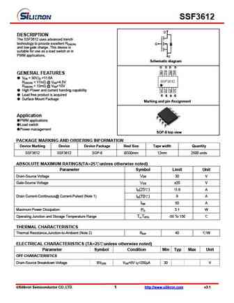
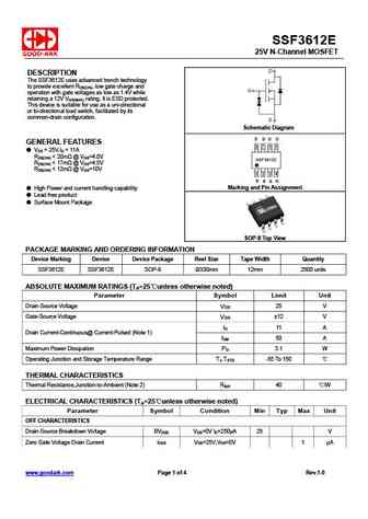
SSF3612 D DESCRIPTION The SSF3612 uses advanced trench technology to provide excellent RDS(ON) G and low gate charge .This device is suitable for use as a load switch or in PWM applications. S Schematic diagram GENERAL FEATURES VDS = 30V,ID =11.6A RDS(ON)
ssf3617.pdf
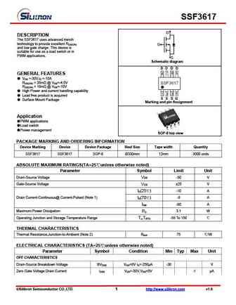
SSF3617 D DESCRIPTION The SSF3617 uses advanced trench technology to provide excellent RDS(ON) G and low gate charge .This device is suitable for use as a load switch or in PWM applications. S Schematic diagram GENERAL FEATURES VDS =-30V,ID =-10A RDS(ON)
ssf3610.pdf

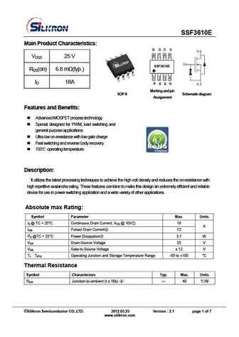
SSF3610 D DESCRIPTION The SSF3610 uses advanced trench technology to provide excellent RDS(ON) G and low gate charge .This device is suitable for use as a load switch or in PWM applications. S Schematic diagram GENERAL FEATURES VDS = 30V,ID =11A RDS(ON)

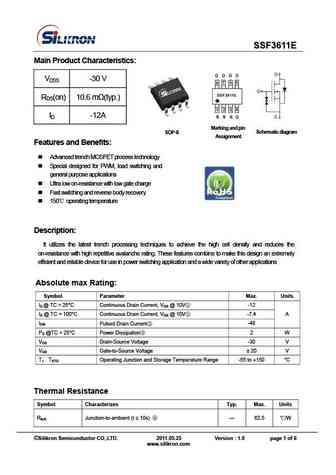
Другие IGBT... SSF3604, SSF3605S, SSF3606, SSF3610, SSF3610E, SSF3611E, SSF3612, SSF3615, MMIS60R580P, SSF3617, SSF3620, SSF3624, SSF3626, SSF3637, SSF3637S, SSF3639C, SSF3641
🌐 : EN ES РУ

Список транзисторов
Обновления
MOSFET: FTF30P35D | FTF25N35DHVT | FTF15N35D | FTE15C35G | FTP02P15G | FTE02P15G | AKF30N5P0SX | AKF30N10S | AKF20P45D | CM4407 | CM3407 | CM3400 | SVF11N65F | SVF11N65T | FKBB3105 | EHBA036R1
Popular searches
2sc1678 | irf4115 | 2sc828 replacement | 2sd669 datasheet | c102 transistor | bt152 datasheet | 2sa1302 datasheet | mpsa13 transistor equivalent