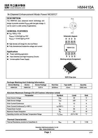
4410. Аналоги и основные параметры
Наименование производителя: 4410
Тип транзистора: MOSFET
Полярность: N
Предельные значения
Pd ⓘ - Максимальная рассеиваемая мощность: 2.5 W
|Vds|ⓘ - Максимально допустимое напряжение сток-исток: 30 V
|Vgs|ⓘ - Максимально допустимое напряжение затвор-исток: 20 V
|Id| ⓘ - Максимально допустимый постоянный ток стока: 10 A
Tj ⓘ - Максимальная температура канала: 150 °C
Электрические характеристики
RDSonⓘ - Сопротивление сток-исток открытого транзистора: 0.014 Ohm
Тип корпуса: SOP8
Аналог (замена) для 4410
- подборⓘ MOSFET транзистора по параметрам
4410 даташит
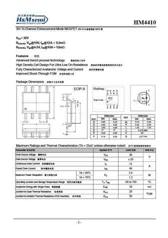
4410.pdf
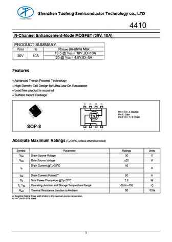
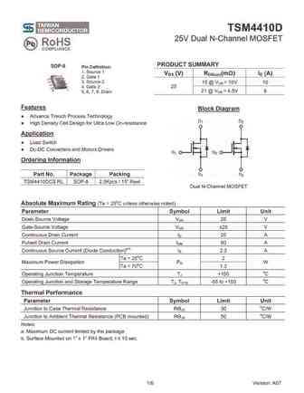
Shenzhen Tuofeng Semiconductor Technology co., LTD 4410 N-Channel Enhancement-Mode MOSFET (30V, 10A) PRODUCT SUMMARY VDSS ID RDS(on) (m-ohm) Max 13.5 @ VGS = 10V ,ID=10A 30V 10A 20 @ VGS = 4.5V,ID=5A Features Advanced Trench Process Technology High Density Cell Design for Ultra Low On-Resistance Lead free product is acquired Surface mount Package Pin 1 /
4410.pdf
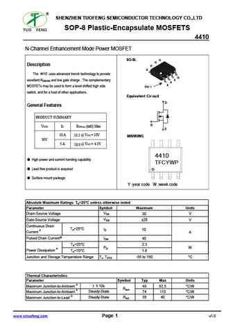
SHENZHEN TUOFENG SEMICONDUCTOR TECHNOLOGY CO.,LTD SOP-8 Plastic-Encapsulate MOSFETS 4410 N-Channel Enhancement Mode Power MOSFET SO-8L D D Description D D The 4410 uses advanced trench technology to provide G G S excellent RDS(ON) and low gate charge . The complementary S S S S MOSFETs may be used to form a level shifted high side SO-8 S Pin 1 switch, and for a host o
me4410ad.pdf
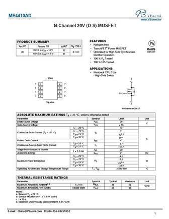
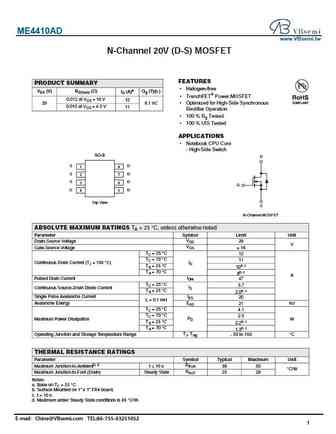
ME4410AD www.VBsemi.tw N-Channel 20V (D-S) MOSFET FEATURES PRODUCT SUMMARY Halogen-free VDS (V) RDS(on) ( ) ID (A)a Qg (Typ.) TrenchFET Power MOSFET 0.012 at VGS = 10 V 12 20 6.1 nC Optimized for High-Side Synchronous 0.015 at VGS = 4.5 V 11 Rectifier Operation 100 % Rg Tested 100 % UIS Tested APPLICATIONS Notebook CPU Core - High-Side Switch SO
me4410a.pdf
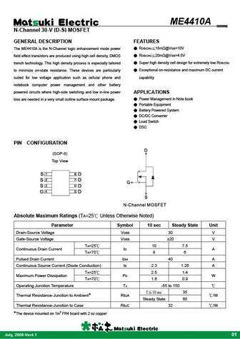
ME4410A N-Channel 30-V (D-S) MOSFET GENERAL DESCRIPTION FEATURES RDS(ON) 18m @VGS=10V The ME4410A is the N-Channel logic enhancement mode power RDS(ON) 20m @VGS=4.5V field effect transistors are produced using high cell density, DMOS Super high density cell design for extremely low RDS(ON) trench technology. This high density process is especially tailored
2n4410re.pdf
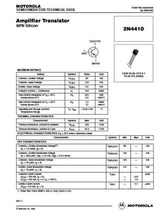
MOTOROLA Order this document SEMICONDUCTOR TECHNICAL DATA by 2N4410/D Amplifier Transistor NPN Silicon 2N4410 COLLECTOR 3 2 BASE 1 EMITTER 1 2 3 MAXIMUM RATINGS CASE 29 04, STYLE 1 Rating Symbol Value Unit TO 92 (TO 226AA) Collector Emitter Voltage VCEO 80 Vdc Collector Base Voltage VCBO 120 Vdc Emitter Base Voltage VEBO 5.0 Vdc Collector Current Continuou
irfb4410pbf irfs4410pbf irfsl4410pbf.pdf
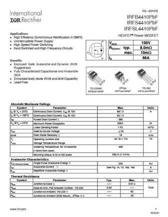
PD - 95707E IRFB4410PbF IRFS4410PbF IRFSL4410PbF Applications HEXFET Power MOSFET l High Efficiency Synchronous Rectification in SMPS l Uninterruptible Power Supply D VDSS 100V l High Speed Power Switching RDS(on) typ. 8.0m l Hard Switched and High Frequency Circuits G max. 10m ID S 88A Benefits l Improved Gate, Avalanche and Dynamic dV/dt Ruggedness l Fully Characterized
auirfb4410.pdf
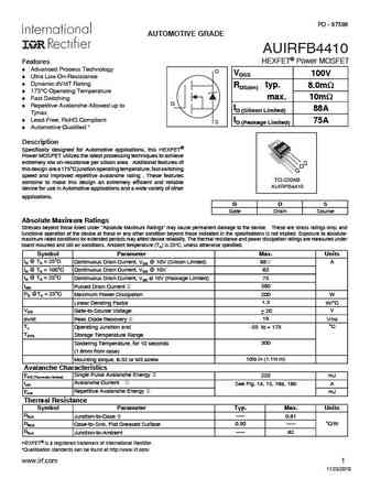
PD - 97598 AUTOMOTIVE GRADE AUIRFB4410 HEXFET Power MOSFET Features Advanced Process Technology D VDSS 100V Ultra Low On-Resistance Dynamic dV/dT Rating RDS(on) typ. 8.0m 175 C Operating Temperature max. 10m Fast Switching G Repetitive Avalanche Allowed up to ID (Silicon Limited) 88A Tjmax Lead-Free, RoHS Compliant ID (Package Limited)
irfi4410zpbf.pdf
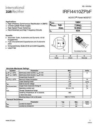
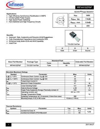
PD - 97475A IRFI4410ZPbF HEXFET Power MOSFET Applications VDSS 100V l High Efficiency Synchronous Rectification in SMPS RDS(on) typ. 7.9m l Uninterruptible Power Supply l High Speed Power Switching max. 9.3m l Hard Switched and High Frequency Circuits ID 43A Benefits D D l Improved Gate, Avalanche and Dynamic dV/dt Ruggedness l Fully Characterized Capacitance and Avala
auirfs4410z auirfsl4410z.pdf
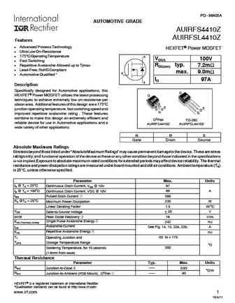
PD - 96405A AUTOMOTIVE GRADE AUIRFS4410Z AUIRFSL4410Z Features l Advanced Process Technology HEXFET Power MOSFET l Ultra Low On-Resistance l 175 C Operating Temperature D VDSS 100V l Fast Switching l Repetitive Avalanche Allowed up to Tjmax RDS(on) typ. 7.2m l Lead-Free, RoHS Compliant max. 9.0m G l Automotive Qualified * ID 97A S Description Specifically desig
irfb4410zpbf irfs4410zpbf irfsl4410zpbf.pdf
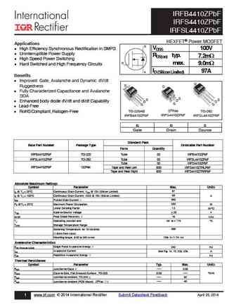
IRFB4410ZPbF IRFS4410ZPbF IRFSL4410ZPbF HEXFET Power MOSFET Applications D VDSS l High Efficiency Synchronous Rectification in SMPS 100V l Uninterruptible Power Supply RDS(on) typ. 7.2m l High Speed Power Switching G max. 9.0m l Hard Switched and High Frequency Circuits ID (Silicon Limited) 97A S Benefits l Improved Gate, Avalanche and Dynamic dV/dt D D Ruggedness D l
si4410dy.pdf
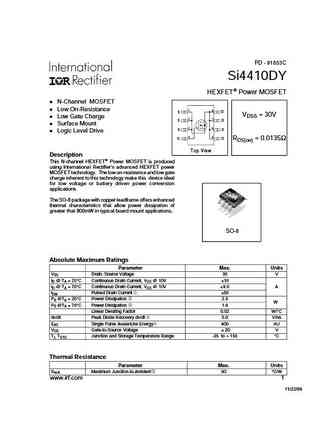
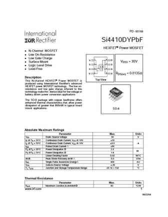
PD - 91853C Si4410DY HEXFET Power MOSFET N-Channel MOSFET A A Low On-Resistance 1 8 S D VDSS = 30V Low Gate Charge 2 7 S D Surface Mount 3 6 S D Logic Level Drive 4 5 G D RDS(on) = 0.0135 Top View Description This N-channel HEXFET Power MOSFET is produced using International Rectifier's advanced HEXFET power MOSFET technology. The low on-resistance and low gat
irfb4410.pdf
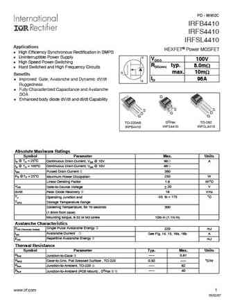
PD - 96902C IRFB4410 IRFS4410 IRFSL4410 Applications HEXFET Power MOSFET l High Efficiency Synchronous Rectification in SMPS l Uninterruptible Power Supply D VDSS 100V l High Speed Power Switching RDS(on) typ. 8.0m l Hard Switched and High Frequency Circuits G max. 10m Benefits ID 96A l Improved Gate, Avalanche and Dynamic dV/dt S Ruggedness l Fully Characterized Capacita
irfi4410zgpbf.pdf
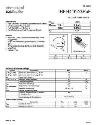
PD - 96372 IRFI4410ZGPbF HEXFET Power MOSFET Applications VDSS 100V l High Efficiency Synchronous Rectification in SMPS RDS(on) typ. 7.9m l Uninterruptible Power Supply l High Speed Power Switching max. 9.3m l Hard Switched and High Frequency Circuits ID 43A Benefits D D l Improved Gate, Avalanche and Dynamic dV/dt Ruggedness l Fully Characterized Capacitance and Avalanche
irfp4410zpbf.pdf
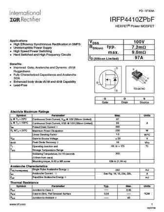
PD - 97309A IRFP4410ZPbF HEXFET Power MOSFET Applications VDSS 100V l High Efficiency Synchronous Rectification in SMPS RDS(on) typ. l Uninterruptible Power Supply 7.2m l High Speed Power Switching max. 9.0m l Hard Switched and High Frequency Circuits ID (Silicon Limited) 97A Benefits l Improved Gate, Avalanche and Dynamic dV/dt D D Ruggedness l Fully Characterized Cap
irfs4410pbf irfsl4410pbf.pdf
PD - 95707E IRFB4410PbF IRFS4410PbF IRFSL4410PbF Applications HEXFET Power MOSFET l High Efficiency Synchronous Rectification in SMPS l Uninterruptible Power Supply D VDSS 100V l High Speed Power Switching RDS(on) typ. 8.0m l Hard Switched and High Frequency Circuits G max. 10m ID S 88A Benefits l Improved Gate, Avalanche and Dynamic dV/dt Ruggedness l Fully Characterized
irfb4410zgpbf.pdf
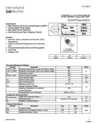
PD - 96213 IRFB4410ZGPbF HEXFET Power MOSFET D Applications VDSS 100V l High Efficiency Synchronous Rectification in SMPS RDS(on) typ. l Uninterruptible Power Supply 7.2m l High Speed Power Switching G max. 9.0m l Hard Switched and High Frequency Circuits ID (Silicon Limited) 97A S Benefits D l Improved Gate, Avalanche and Dynamic dV/dt Ruggedness l Fully Characterized C
irfb4410 irfs4410 irfsl4410.pdf
PD - 96902C IRFB4410 IRFS4410 IRFSL4410 Applications HEXFET Power MOSFET l High Efficiency Synchronous Rectification in SMPS l Uninterruptible Power Supply D VDSS 100V l High Speed Power Switching RDS(on) typ. 8.0m l Hard Switched and High Frequency Circuits G max. 10m Benefits ID 96A l Improved Gate, Avalanche and Dynamic dV/dt S Ruggedness l Fully Characterized Capacita
mp4410 .pdf
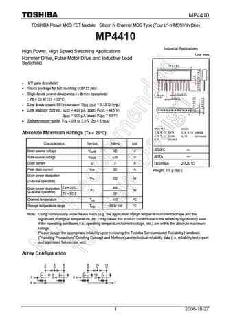
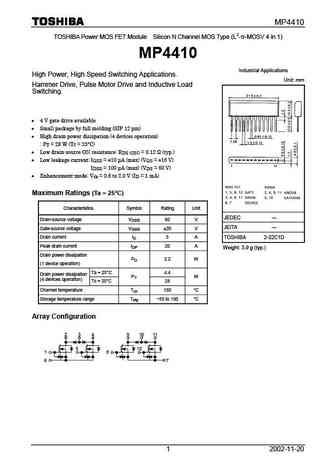
MP4410 TOSHIBA Power MOS FET Module Silicon N Channel MOS Type (Four L2- -MOSV in One) MP4410 Industrial Applications High Power, High Speed Switching Applications Unit mm Hammer Drive, Pulse Motor Drive and Inductive Load Switching 4-V gate drivability Small package by full molding (SIP 12 pin) High drain power dissipation (4-device operation) PT = 28 W (T
mp4410.pdf
MP4410 TOSHIBA Power MOS FET Module Silicon N Channel MOS Type (L2- -MOSV 4 in 1) MP4410 Industrial Applications High Power, High Speed Switching Applications. Unit mm Hammer Drive, Pulse Motor Drive and Inductive Load Switching. 4 V gate drive available Small package by full molding (SIP 12 pin) High drain power dissipation (4 devices operation) PT = 28 W
fds4410.pdf
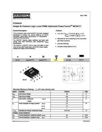
April 1998 FDS4410 Single N-Channel Logic Level PWM Optimized PowerTrenchTM MOSFET General Description Features This N-Channel Logic Level MOSFET has been designed 10 A, 30 V. RDS(ON) = 0.0135 @ VGS = 10 V specifically to improve the overall efficiency of DC/DC RDS(ON) = 0.0200 @ VGS = 4.5 V. converters using either synchronous or conventional switching PWM controllers. O
hp4410dy.pdf
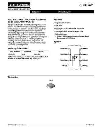
HP4410DY Data Sheet December 2001 10A, 30V, 0.0135 Ohm, Single N-Channel, Features Logic Level Power MOSFET Logic Level Gate Drive This power MOSFET is manufactured using an innovative 10A, 30V process. This advanced process technology achieves the rDS(ON) = 0.0135 at ID = 10A, VGS = 10V lowest possible on-resistance per silicon area, resulting in outstanding perform
fds4410a.pdf
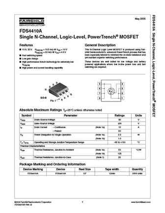
May 2005 FDS4410A Single N-Channel, Logic-Level, PowerTrench MOSFET Features General Description 10 A, 30 V. RDS(ON) = 13.5 m @ VGS = 10 V This N-Channel Logic Level MOSFET is produced using Fair- RDS(ON) = 20 m @ VGS = 4.5 V child Semiconductor s advanced PowerTrench process that has been especially tailored to minimize the on-state resistance and Fast switching speed
fqs4410tf.pdf
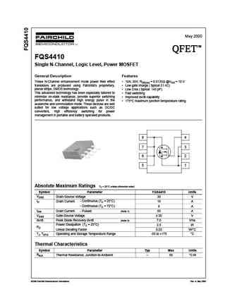
May 2000 TM QFET QFET QFET QFET FQS4410 Single N-Channel, Logic Level, Power MOSFET General Description Features These N-Channel enhancement mode power field effect 10A, 30V, RDS(on) = 0.0135 @VGS = 10 V transistors are produced using Fairchild s proprietary, Low gate charge ( typical 21 nC) planar stripe, DMOS technology. Low Crss ( typical 145 pF) This advanced t
2n4410.pdf
Discrete POWER & Signal Technologies 2N4410 C TO-92 B E NPN General Purpose Amplifier This device is designed for use as general purpose amplifiers and switches requiring collector currents to 50 mA. Sourced from Process 16. See 2N5551 for characteristics. Absolute Maximum Ratings* TA = 25 C unless otherwise noted Symbol Parameter Value Units VCEO Collector-Emitter Voltage 80 V V
fdr4410.pdf
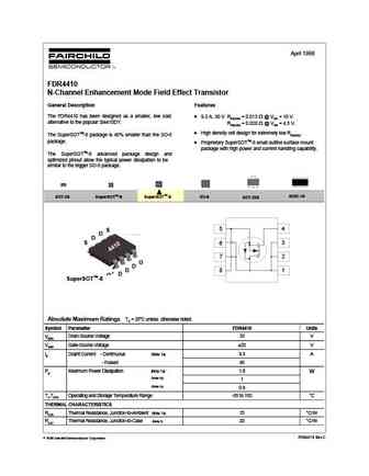
April 1998 FDR4410 N-Channel Enhancement Mode Field Effect Transistor General Description Features The FDR4410 has been designed as a smaller, low cost 9.3 A, 30 V. RDS(ON) = 0.013 @ VGS = 10 V alternative to the popular Si4410DY. RDS(ON) = 0.020 @ VGS = 4.5 V. High density cell design for extremely low RDS(ON). The SuperSOTTM-8 package is 40% smaller than the SO-8 package
si4410bdy.pdf
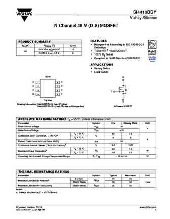
Si4410BDY Vishay Siliconix N-Channel 30-V (D-S) MOSFET FEATURES PRODUCT SUMMARY Halogen-free According to IEC 61249-2-21 VDS (V) RDS(on) ( )ID (A) Definition 0.0135 at VGS = 10 V 10 TrenchFET Power MOSFET 30 0.020 at VGS = 4.5 V 8 100 % Rg Tested Compliant to RoHS Directive 2002/95/EC APPLICATIONS Battery Switch Load Switch SO-8 D S D 1
si4410dypbf si4410dytrpbf.pdf
PD - 95168 Si4410DYPbF HEXFET Power MOSFET l N-Channel MOSFET l Low On-Resistance A l Low Gate Charge A 1 8 S D VDSS = 30V l Surface Mount 2 7 S D l Logic Level Drive 3 6 l Lead-Free S D 4 5 G D RDS(on) = 0.0135 Description Top View This N-channel HEXFET Power MOSFET is produced using International Rectifier's advanced HEXFET power MOSFET technology. The low on- re
si4410dy.pdf
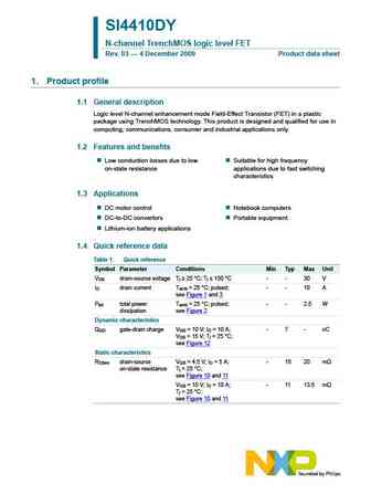
SI4410DY N-channel TrenchMOS logic level FET Rev. 03 4 December 2009 Product data sheet 1. Product profile 1.1 General description Logic level N-channel enhancement mode Field-Effect Transistor (FET) in a plastic package using TrenchMOS technology. This product is designed and qualified for use in computing, communications, consumer and industrial applications only. 1.2 Features a
sq4410ey.pdf
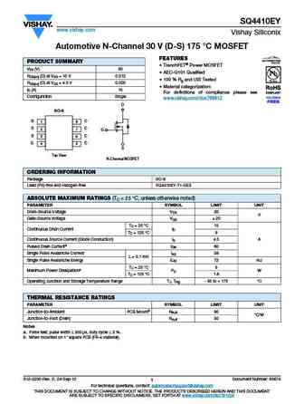
SQ4410EY www.vishay.com Vishay Siliconix Automotive N-Channel 30 V (D-S) 175 C MOSFET FEATURES PRODUCT SUMMARY TrenchFET Power MOSFET VDS (V) 30 AEC-Q101 Qualified RDS(on) ( ) at VGS = 10 V 0.012 100 % Rg and UIS Tested RDS(on) ( ) at VGS = 4.5 V 0.020 Material categorization ID (A) 15 For definitions of compliance please see Configuration Single www
irfi4410zpbf.pdf
IRFI4410ZPbF HEXFET Power MOSFET Applications VDSS 100V High Efficiency Synchronous Rectification in SMPS Uninterruptible Power Supply RDS(on) typ. 7.9m High Speed Power Switching Hard Switched and High Frequency Circuits RDS(on) max. 9.3m ID 43A Benefits Improved Gate, Avalanche and Dynamic dV/dt Ruggedness Fully Characterized Capac
si4410dypbf.pdf
PD - 95168 Si4410DYPbF HEXFET Power MOSFET l N-Channel MOSFET l Low On-Resistance A l Low Gate Charge A 1 8 S D VDSS = 30V l Surface Mount 2 7 S D l Logic Level Drive 3 6 l Lead-Free S D 4 5 G D RDS(on) = 0.0135 Description Top View This N-channel HEXFET Power MOSFET is produced using International Rectifier's advanced HEXFET power MOSFET technology. The low on- re
2sc4410.pdf
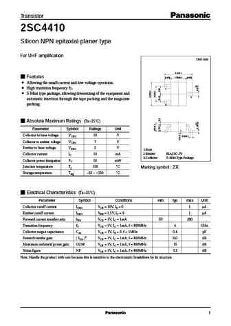
Transistor 2SC4410 Silicon NPN epitaxial planer type For UHF amplification Unit mm 2.1 0.1 Features 0.425 1.25 0.1 0.425 Allowing the small current and low voltage operation. High transition frequency fT. 1 S-Mini type package, allowing downsizing of the equipment and 3 automatic insertion through the tape packing and the magazine packing. 2 Absolute Maximum Ratings (Ta=25 C
2sc4410 e.pdf
Transistor 2SC4410 Silicon NPN epitaxial planer type For UHF amplification Unit mm 2.1 0.1 Features 0.425 1.25 0.1 0.425 Allowing the small current and low voltage operation. High transition frequency fT. 1 S-Mini type package, allowing downsizing of the equipment and 3 automatic insertion through the tape packing and the magazine packing. 2 Absolute Maximum Ratings (Ta=25 C
ut4410.pdf
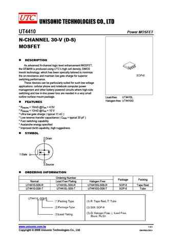
UNISONIC TECHNOLOGIES CO., LTD UT4410 Power MOSFET N-CHANNEL 30-V (D-S) MOSFET DESCRIPTION As advanced N-channel logic level enhancement MOSFET, the UT4410 is produced using UTC s high cell density, DMOS trench technology. which has been specially tailored to minimize the on-resistance and maintain low gate charge for superior switching performance. These devices can be
itc14410.pdf
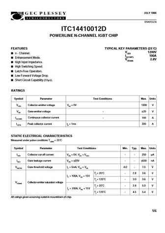
JULY 1996 IT14410012D PRELIMINARY DATA DS4372-2.6 ITC14410012D POWERLINE N-CHANNEL IGBT CHIP FEATURES TYPICAL KEY PARAMETERS (25 C) VCES 1200V n - Channel. IC(CONT) 100A Enhancement Mode. VCE(sat) 2.8V High Input Impedance. High Switching Speed. Latch-Free Operation. Low Forward Voltage Drop. Short Circuit Capability (10 s). RATINGS Symbol Parameter Test Conditions Ma
ssg4410n.pdf
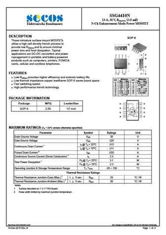
SSG4410N 13 A, 30 V, RDS(ON) 13.5 m N-Ch Enhancement Mode Power MOSFET Elektronische Bauelemente DESCRIPTION SOP-8 These miniature surface mount MOSFETs utilize a high cell density trench process to B provide low RDS(on) and to ensure minimal power loss and heat dissipation. Typical applications are DC-DC converters and power L D management in portable and battery-pow
cjd4410.pdf
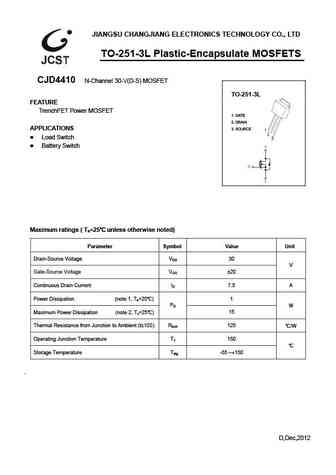
JIANGSU CHANGJIANG ELECTRONICS TECHNOLOGY CO., LTD TO-251-3L Plastic-Encapsulate MOSFETS CJD4410 N-Channel 30-V(D-S) MOSFET TO-2 51-3L FEATURE TrenchFET Power MOSFET 1. GATE 2. DRAIN APPLICATIONS 3. SOURCE Load Switch Battery Switch Maximum ratings ( Ta=25 unless otherwise noted) Parameter Symbol Value Unit Drain-Source Voltage VDS 30 V Gate-Source Voltage
cjq4410.pdf
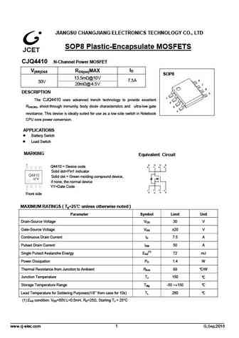
JIANGSU CHANGJIANG ELECTRONICS TECHNOLOGY CO., LTD SOP8 Plastic-Encapsulate MOSFETS CJQ4410 N-Channel Power MOSFET ID V(BR)DSS R DS(on) MAX SOP8 13.5 10 m @ V 7.5A 30V 20m @ 4.5V DESCRIPTION The CJQ4410 uses advanced trench technology to provide excellent RDS(ON), shoot-through immunity, body diode characteristics and ultra-low gate resistance. This device is ideall
pt4410.pdf
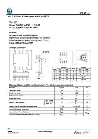
PT4410 30V N-Channel Enhancement Mode MOSFET VDS= 30V RDS(ON), Vgs@10V, Ids@12A = 10.5m RDS(ON), Vgs@4.5V, Ids@12A = 15m Features Advanced trench process technology High Density Cell Design For Ultra Low On-Resistance Fully Characterized Avalanche Voltage and Current Improved Shoot-Through FOM Package Dimensions D D D D 8 7 6 5 1 2 3 4 S S S G Millimeter Millimeter
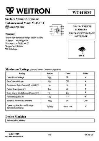
wt4410m.pdf
WT4410M Surface Mount N-Channel Enhancement Mode MOSFET DRAIN CURRENT P b Lead(Pb)-Free 10 AMPERS DRAIN SOUCE VOLTAGE Features 30 VOLTAGE *Super high dense cell design for low R DS(ON) RDS(ON)
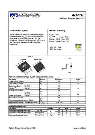
ao4410.pdf
AO4410 30V N-Channel MOSFET General Description Product Summary The AO4410 uses advanced trench technology to VDS (V) = 30V provide excellent RDS(ON), shoot-through immunity, ID = 18A (VGS = 10V) body diode characteristics and ultra-low gate RDS(ON)
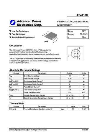
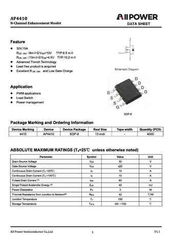
ap4410m.pdf
AP4410M Advanced Power N-CHANNEL ENHANCEMENT MODE Electronics Corp. POWER MOSFET Low On-Resistance BVDSS 30V D D Fast Switching D RDS(ON) 13.5m D Simple Drive Requirement ID 10A G S S SO-8 S Description D D The Advanced Power MOSFETs from APEC provide the designer with the best combination of fast switching, rugged
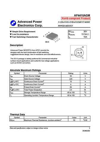
ap4410agm.pdf
AP4410AGM RoHS-compliant Product Advanced Power N-CHANNEL ENHANCEMENT MODE Electronics Corp. POWER MOSFET Simple Drive Requirement BVDSS 30V D D Low On-resistance RDS(ON) 13.5m D D Fast Switching Characteristic ID 10A G S S S SO-8 Description D Advanced Power MOSFETs from APEC provide the designer with the best combination of fast switching, ruggedized device d
ap4410agm-hf.pdf
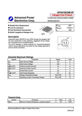
AP4410AGM-HF Halogen-Free Product Advanced Power N-CHANNEL ENHANCEMENT MODE Electronics Corp. POWER MOSFET Simple Drive Requirement BVDSS 30V D D Low On-resistance RDS(ON) 13.5m D D Fast Switching Characteristic ID 10A G S RoHS Compliant & Halogen-Free S S SO-8 Description D Advanced Power MOSFETs from APEC provide the designer with the best combination of
ap4410gm.pdf
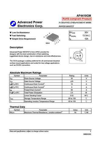
AP4410GM RoHS-compliant Product Advanced Power N-CHANNEL ENHANCEMENT MODE Electronics Corp. POWER MOSFET Low On-Resistance BVDSS 30V D D Fast Switching D RDS(ON) 13.5m D Simple Drive Requirement ID 10A G S S SO-8 S Description D D Advanced Power MOSFETs from APEC provide the designer with the best combination of fast switching, ruggedized device design, low on-
am4410n.pdf
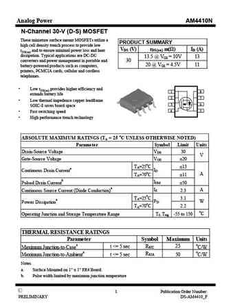
Analog Power AM4410N N-Channel 30-V (D-S) MOSFET These miniature surface mount MOSFETs utilize a PRODUCT SUMMARY high cell density trench process to provide low VDS (V) rDS(on) m( ) ID (A) rDS(on) and to ensure minimal power loss and heat dissipation. Typical applications are DC-DC 13.5 @ VGS = 10V 13 converters and power management in portable and 30 20 @ VGS = 4.5V 11 battery
mtn4410v8.pdf
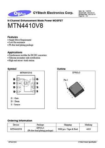
Spec. No. C397V8 Issued Date 2012.03.14 CYStech Electronics Corp. Revised Date 2012.03.15 Page No. 1/9 N-Channel Enhancement Mode Power MOSFET MTN4410V8 Features Single Drive Requirement Low On-resistance Pb-free lead plating package Applications Synchronous rectifier for DC/DC converters Telecom secondary side rectification High end s
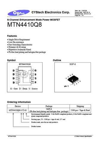
mtn4410q8.pdf
Spec. No. C397Q8 Issued Date 2007.06.14 CYStech Electronics Corp. Revised Date 2014.01.23 Page No. 1/8 N-Channel Enhancement Mode Power MOSFET MTN4410Q8 Features Single Drive Requirement Low On-resistance Fast Switching Characteristic Dynamic dv/dt rating Repetitive Avalanche Rated Pb-free lead plating and halogen-free package Symbol O
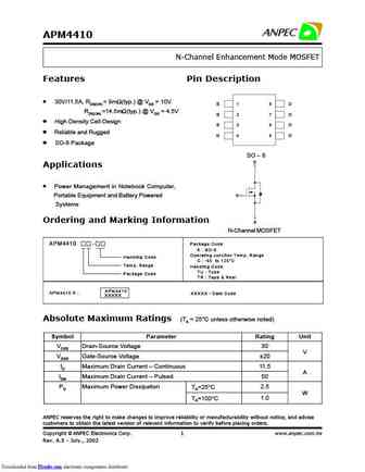
apm4410.pdf
APM4410 N-Channel Enhancement Mode MOSFET Features Pin Description 30V/11.5A, RDS(ON) = 9m (typ.) @ VGS = 10V S 1 8 D RDS(ON) =14.5m (typ.) @ VGS = 4.5V S 2 7 D High Density Cell Design S 3 6 D Reliable and Rugged G 45 D SO-8 Package SO - 8 D Applications Power Management in Notebook Computer, G
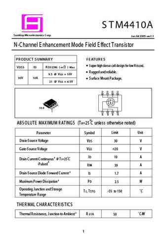
stm4410a.pdf
S T M4410A S amHop Microelectronics C orp. J an 04 2005 ver1.1 N-C hannel E nhancement Mode Field E ffect Transistor P R ODUC T S UMMAR Y F E AT UR E S S uper high dense cell design for low R DS (ON). V DS S ID R DS (ON) ( m W ) Max R ugged and reliable. 9.5 @ V G S = 10V 30V 10A S urface Mount Package. 21 @ V G S = 4.5V S O-8 1 ABS OLUTE MAXIMUM R ATINGS (TA=25 C unless other
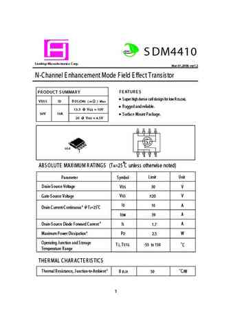
sdm4410.pdf
Green Product S DM4410 S amHop Microelectronics C orp. Mar.01,2006 ver1.2 N-Channel E nhancement Mode Field E ffect Transistor PR ODUC T S UMMAR Y F E ATUR E S S uper high dense cell design for low R DS (ON). VDS S ID R DS (ON) ( m ) Max R ugged and reliable. 13.5 @ VG S = 10V 30V 10A S urface Mount Package. 20 @ VG S = 4.5V S O-8 1 ABS OLUTE MAXIMUM R ATINGS (TA=25 C unless
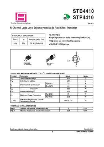
stb4410 stp4410.pdf
STB4410 Green Product STP4410 a S mHop Microelectronics C orp. Ver 1.0 N-Channel Logic Level Enhancement Mode Field Effect Transistor FEATURES PRODUCT SUMMARY Super high dense cell design for extremely low RDS(ON). VDSS ID RDS(ON) (m ) Typ High power and current handling capability. 100V 75A 7.0 @ VGS=10V TO-220 & TO-263 package. D G STB SERIES STP SERIES TO-263(DD-PAK) TO-
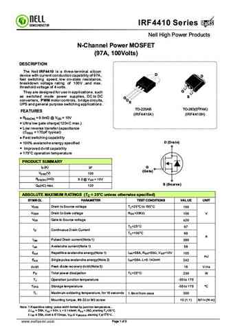
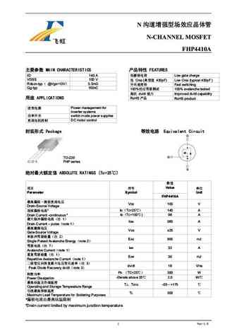
irf4410a irf4410h.pdf
RoHS IRF4410 Series RoHS SEMICONDUCTOR Nell High Power Products N-Channel Power MOSFET (97A, 100Volts) DESCRIPTION The Nell IRF4410 is a three-terminal silicon D device with current conduction capability of 97A, D fast switching speed, low on-state resistance, breakdown voltage rating of 100V ,and max. threshold voltage of 4 volts. G They are designed for use in application
ftk4410d.pdf
SEMICONDUCTOR FTK4410D TECHNICAL DATA N-Channel MOSFET A I DESCRIPTION C J The FTK410D uses advanced trench te chnology to provide excellent RDS(ON) and low gate charge. DIM MILLIMETERS This device is suitable for use as a load switch A 6 50 0 2 B 5 60 0 2 or in PWM applications. C 5 20 0 2 D 1 50 0 2 E 2 70 0 2 F 2 30 0 1 H H 1 00 MAX I 2 30 0
ftk4410.pdf
SEMICONDUCTOR FTK4410 TECHNICAL DATA DESCRIPTION N-Channel MOSFET The FTK4410 uses advanced trench technology to provide excellent RDS(ON), low gate charge .It has been optimized for power management applications requiring a wide range of gave drive voltage ratings (4.5V 25V). Schematic diagram D D D D GENERAL FEATURES 7 6 5 8 VDS = 30V,I = 7.5A D RDS(ON)
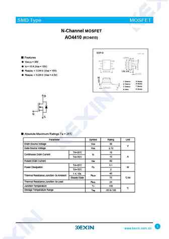
ao4410.pdf
SMD Type MOSFET N-Channel MOSFET AO4410 (KO4410) SOP-8 Features VDS (V) = 30V ID = 18 A (VGS = 10V) RDS(ON) 5.5m (VGS = 10V) 1.50 0.15 RDS(ON) 6.2m (VGS = 4.5V) 1 Source 5 Drain 6 Drain 2 Source 7 Drain 3 Source 8 Drain 4 Gate D G S Absolute Maximum Ratings Ta = 25 Parameter Symbol Rating Unit Drain-Source Voltage VDS 30 V Gat
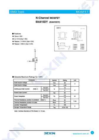
si4410dy.pdf
SMD Type MOSFET N-Channel MOSFET SI4410DY (KI4410DY) SOP-8 Features VDS (V) = 30V ID = 10 A (VGS = 10V) 1.50 0.15 RDS(ON) 13.5m (VGS = 10V) RDS(ON) 20m (VGS = 4.5V) 1 Source 5 Drain 6 Drain 2 Source 7 Drain 3 Source 8 Drain 4 Gate D G S Absolute Maximum Ratings Ta = 25 Parameter Symbol Rating Unit Drain-Source Voltage VDS 30 V
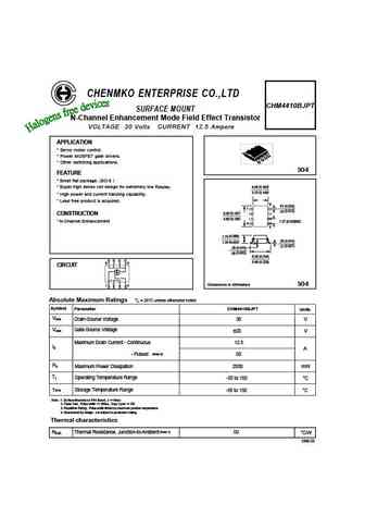
chm4410bjgp.pdf
CHENMKO ENTERPRISE CO.,LTD CHM4410BJPT SURFACE MOUNT N-Channel Enhancement Mode Field Effect Transistor VOLTAGE 30 Volts CURRENT 12.5 Ampere APPLICATION * Servo motor control. * Power MOSFET gate drivers. * Other switching applications. SO-8 FEATURE * Small flat package. (SO-8 ) ( ) * Super high dense cell design for extremely low RDS(ON). 4.06 0.160 ( ) 3.70 0.146 * High pow
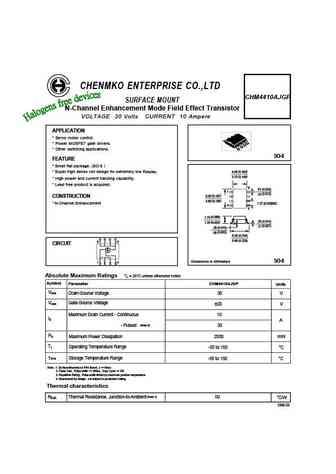
chm4410ajgp.pdf
CHENMKO ENTERPRISE CO.,LTD CHM4410AJGP SURFACE MOUNT N-Channel Enhancement Mode Field Effect Transistor VOLTAGE 30 Volts CURRENT 10 Ampere APPLICATION * Servo motor control. * Power MOSFET gate drivers. * Other switching applications. SO-8 FEATURE * Small flat package. (SO-8 ) ( ) * Super high dense cell design for extremely low RDS(ON). 4.06 0.160 ( ) 3.70 0.146 * High power
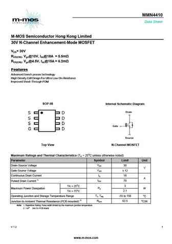
mmn4410.pdf
MMN4410 Data Sheet M-MOS Semiconductor Hong Kong Limited 30V N-Channel Enhancement-Mode MOSFET VDS= 30V RDS(ON), Vgs@10V, Ids@18A = 5.5m RDS(ON), Vgs@4.5V, Ids@15A = 6.2m Features Advanced trench process technology High Density Cell Design For Ultra Low On-Resistance Improved Shoot-Through FOM SOP-08 Internal Schematic Diagram Drain Gate Source Top View N-Channel MOSFET
ssm4410m.pdf
SSM4410M N-CHANNEL ENHANCEMENT MODE POWER MOSFET Low on-resistance BV 30V DSS D D Fast switching D RDS(ON) 13.5m D Simple drive requirement I 10A D G S S SO-8 S Description D Power MOSFETs from Silicon Standard provide the designer with the best combination of fast switching, ruggedized device design, low on-resistance and cost-effectiveness. G S The SO-8 package is wid
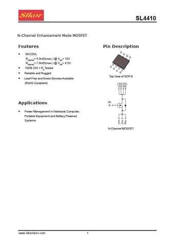
sl4410.pdf
SL4410 N-Channel Enhancement Mode MOSFET Features Pin Description D D 30V/20A, D D RDS(ON)= 5.9m (max.) @ VGS= 10V RDS(ON)= 7.9m (max.) @ VGS= 4.5V S 100% UIS + Rg Tested S S G Reliable and Rugged Top View of SOP-8 Lead Free and Green Devices Available (RoHS Compliant) ( 5,6,7,8 ) D D D D (4) Applications G Power Management in Notebook Computer, Portable Equipm
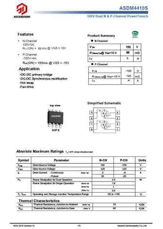
asdm4410s.pdf
ASDM4410S 100V Dual N & P-Channel PowerTrench Features Product Summary N-Channel V DS 100 V V DS V 100 95 95 R DS(on),Typ@ VGS=10 V m R DS(on),Typ@ VGS=10 V m 5 I A I D RDS (ON) = 185m @ VGS = -10V P-Channel Application V DS -100 V DC-DC primary bridge 185 R DS(on),Typ@ VGS=-10 V m DC-DC Synchronous rectification I D -4 A Hot
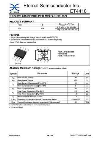
et4410.pdf
Eternal Semiconductor Inc. ET4410 N-Channel Enhancement-Mode MOSFET (30V, 10A) PRODUCT SUMMARY VDSS ID RDS(on) (m ) Typ. 9 @ VGS = 10V, ID=6.9A 30V 10A 13@ VGS = 4.5V, ID=5.8A Features Super high density cell design for extremely low RDS(ON) Exceptional on-resistance and maximum DC current capability Lead Pb -free and halogen-free Pin 1 / 2 / 3 Source Pin 4 Gate
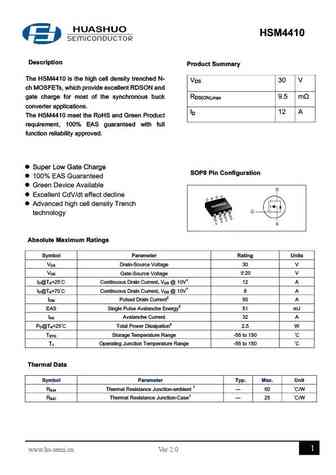
hsm4410.pdf
HSM4410 Description Product Summary The HSM4410 is the high cell density trenched N- VDS 30 V ch MOSFETs, which provide excellent RDSON and gate charge for most of the synchronous buck RDS(ON),max 9.5 m converter applications. ID 12 A The HSM4410 meet the RoHS and Green Product requirement, 100% EAS guaranteed with full function reliability approved. l Super Low Gate C
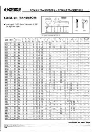
2n4265 2n4400 2n4401 2n4402 2n4403 2n4409 2n4410 2n4424 2n4425 2n4951 2n4952 2n4953 2n4954 2n5087 2n5088 2n5089.pdf
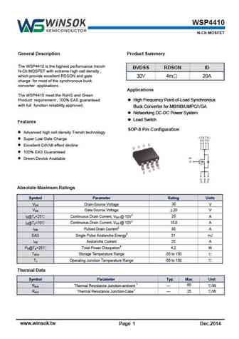
wsp4410.pdf
WSP4410 N-Ch MOSFET General Description Product Summery The WSP4410 is the highest performance trench BVDSS RDSON ID N-Ch MOSFET with extreme high cell density , which provide excellent RDSON and gate 30V 4m 20A charge for most of the synchronous buck converter applications . Applications The WSP4410 meet the RoHS and Green High Frequency Point-of-Load Synchronous Prod
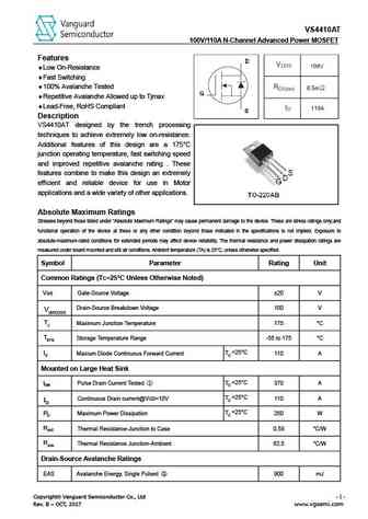
vs4410at.pdf
VS4410AT 100V/110A N-Channel Advanced Power MOSFET Features Low On-Resistance Fast Switching 100% Avalanche Tested Repetitive Avalanche Allowed up to Tjmax Lead-Free, RoHS Compliant Description VS4410AT designed by the trench processing techniques to achieve extremely low on-resistance. Additional features of this design are a 175 C junction opera
sm4410.pdf
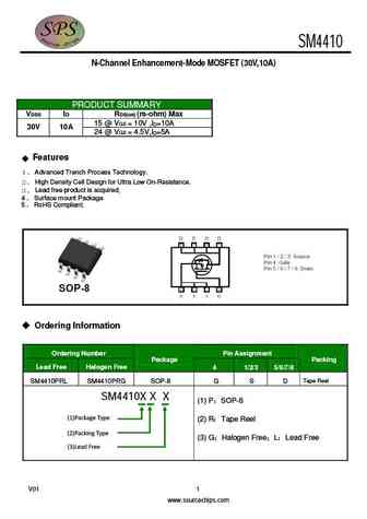
SM4410 N-Channel Enhancement-Mode MOSFET (30V,10A) PRODUCT SUMMARY VDSS ID RDS(on) (m-ohm) Max 15 @ VGS = 10V ,ID=10A 30V 10A 24 @ VGS = 4.5V,ID=5A Features 1 Advanced Trench Process Technology. 2 High Density Cell Design for Ultra Low On-Resistance. 3 Lead free product is acquired . 4 Surface mount Package 5 RoHS Compliant. Ordering
si4410bdy.pdf
SI4410BDY www.VBsemi.tw N-Channel 20V (D-S) MOSFET FEATURES PRODUCT SUMMARY Halogen-free VDS (V) RDS(on) ( ) ID (A)a Qg (Typ.) TrenchFET Power MOSFET 0.012 at VGS = 10 V 12 20 6.1 nC Optimized for High-Side Synchronous 0.015 at VGS = 4.5 V 11 Rectifier Operation 100 % Rg Tested 100 % UIS Tested APPLICATIONS Notebook CPU Core - High-Side Switch S
si4410dy-t1.pdf
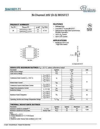
SI4410DY-T1 www.VBsemi.tw N-Channel 20V (D-S) MOSFET FEATURES PRODUCT SUMMARY Halogen-free VDS (V) RDS(on) ( ) ID (A)a Qg (Typ.) TrenchFET Power MOSFET 0.012 at VGS = 10 V 12 20 6.1 nC Optimized for High-Side Synchronous 0.015 at VGS = 4.5 V 11 Rectifier Operation 100 % Rg Tested 100 % UIS Tested APPLICATIONS Notebook CPU Core - High-Side Switch
me4410ad.pdf
ME4410AD www.VBsemi.tw N-Channel 20V (D-S) MOSFET FEATURES PRODUCT SUMMARY Halogen-free VDS (V) RDS(on) ( ) ID (A)a Qg (Typ.) TrenchFET Power MOSFET 0.012 at VGS = 10 V 12 20 6.1 nC Optimized for High-Side Synchronous 0.015 at VGS = 4.5 V 11 Rectifier Operation 100 % Rg Tested 100 % UIS Tested APPLICATIONS Notebook CPU Core - High-Side Switch SO
vbza4410.pdf
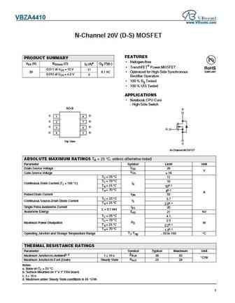
VBZA4410 www.VBsemi.com N-Channel 20V (D-S) MOSFET FEATURES PRODUCT SUMMARY Halogen-free VDS (V) RDS(on) ( ) ID (A)a Qg (Typ.) TrenchFET Power MOSFET 0.011 at VGS = 10 V 11 20 6.1 nC Optimized for High-Side Synchronous 0.015 at VGS = 4.5 V 9 Rectifier Operation 100 % Rg Tested 100 % UIS Tested APPLICATIONS Notebook CPU Core - High-Side Switch SO
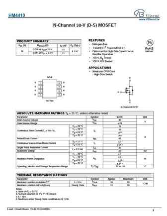
hm4410.pdf
HM4410 www.VBsemi.tw N-Channel 30-V (D-S) MOSFET FEATURES PRODUCT SUMMARY Halogen-free VDS (V) RDS(on) ( ) ID (A)a Qg (Typ.) TrenchFET Power MOSFET 0.008 at VGS = 10 V 13 30 6.1 nC Optimized for High-Side Synchronous 0.011 at VGS = 4.5 V 11 Rectifier Operation 100 % Rg Tested 100 % UIS Tested APPLICATIONS Notebook CPU Core - High-Side Switch SO
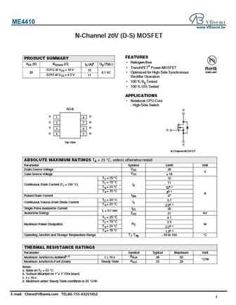
me4410.pdf
ME4410 www.VBsemi.tw N-Channel 20V (D-S) MOSFET FEATURES PRODUCT SUMMARY Halogen-free VDS (V) RDS(on) ( ) ID (A)a Qg (Typ.) TrenchFET Power MOSFET 0.012 at VGS = 10 V 12 20 6.1 nC Optimized for High-Side Synchronous 0.015 at VGS = 4.5 V 11 Rectifier Operation 100 % Rg Tested 100 % UIS Tested APPLICATIONS Notebook CPU Core - High-Side Switch SO-8
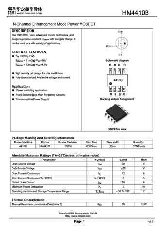
hm4410b.pdf
HM4410B N-Channel Enhancement Mode Power MOSFET DESCRIPTION The HM4410B uses advanced trench technology and design to provide excellent RDS(ON) with low gate charge. It can be used in a wide variety of applications. GENERAL FEATURES VDS =30V,ID =12A RDS(ON)
hm4410a.pdf
HM4410A N-Channel Enhancement Mode Power MOSFET DESCRIPTION The HM4410A uses advanced trench technology and design to provide excellent RDS(ON) with low gate charge. It can be used in a wide variety of applications. GENERAL FEATURES VDS =30V,ID =12A RDS(ON)
irfb4410zg.pdf
isc N-Channel MOSFET Transistor IRFB4410ZG IIRFB4410ZG FEATURES Static drain-source on-resistance RDS(on) 9.0m Enhancement mode Fast Switching Speed 100% avalanche tested Minimum Lot-to-Lot variations for robust device performance and reliable operation DESCRITION reliable device for use in a wide variety of applications ABSOLUTE MAXIMUM RATINGS(T =25 )
irfs4410z.pdf
Isc N-Channel MOSFET Transistor IRFS4410Z FEATURES With To-263(D2PAK) package Low input capacitance and gate charge Low gate input resistance 100% avalanche tested Minimum Lot-to-Lot variations for robust device performance and reliable operation APPLICATIONS Switching applications ABSOLUTE MAXIMUM RATINGS(T =25 ) a SYMBOL PARAMETER VALUE UNIT V Drain-Source Vol
irfs4410.pdf
Isc N-Channel MOSFET Transistor IRFS4410 FEATURES With To-263(D2PAK) package Low input capacitance and gate charge Low gate input resistance 100% avalanche tested Minimum Lot-to-Lot variations for robust device performance and reliable operation APPLICATIONS Switching applications ABSOLUTE MAXIMUM RATINGS(T =25 ) a SYMBOL PARAMETER VALUE UNIT V Drain-Source Volt
irfp4410z.pdf
isc N-Channel MOSFET Transistor IRFP4410Z IIRFP4410Z FEATURES Static drain-source on-resistance RDS(on) 9.0m Enhancement mode Vth =2.0 to 4.0 V (VDS=VGS, ID=250 A) 100% avalanche tested Minimum Lot-to-Lot variations for robust device performance and reliable operation DESCRITION High Efficiency Synchronous Rectification in SMPS Uninterruptible Power Supply
irfsl4410.pdf
isc N-Channel MOSFET Transistor IRFSL4410 FEATURES Static drain-source on-resistance RDS(on) 10m Enhancement mode Fast Switching Speed 100% avalanche tested Minimum Lot-to-Lot variations for robust device performance and reliable operation DESCRITION reliable device for use in a wide variety of applications ABSOLUTE MAXIMUM RATINGS(T =25 ) a SYMBOL PARAME
irfi4410z.pdf
isc N-Channel MOSFET Transistor IRFI4410Z,IIRFI4410Z FEATURES Low drain-source on-resistance RDS(on) 9.3m (max) Enhancement mode Fast Switching Speed 100% avalanche tested Minimum Lot-to-Lot variations for robust device performance and reliable operation DESCRITION Device for use in a wide variety of applications ABSOLUTE MAXIMUM RATINGS(T =25 ) a SYMBOL
irfb4410.pdf
INCHANGE Semiconductor isc N-Channel MOSFET Transistor IRFB4410 IIRFB4410 FEATURES Static drain-source on-resistance RDS(on) 10m Enhancement mode Fast Switching Speed 100% avalanche tested Minimum Lot-to-Lot variations for robust device performance and reliable operation DESCRITION reliable device for use in a wide variety of applications ABSOLUTE MAXIMU
irfb4410z.pdf
INCHANGE Semiconductor isc N-Channel MOSFET Transistor IRFB4410Z IIRFB4410Z FEATURES Static drain-source on-resistance RDS(on) 9.0m Enhancement mode Fast Switching Speed 100% avalanche tested Minimum Lot-to-Lot variations for robust device performance and reliable operation DESCRITION reliable device for use in a wide variety of applications ABSOLUTE MAXIM
irfsl4410z.pdf
INCHANGE Semiconductor isc N-Channel MOSFET Transistor IRFSL4410Z FEATURES Static drain-source on-resistance RDS(on) 9.0m Enhancement mode Fast Switching Speed 100% avalanche tested Minimum Lot-to-Lot variations for robust device performance and reliable operation DESCRITION reliable device for use in a wide variety of applications ABSOLUTE MAXIMUM RATINGS(T
Другие MOSFET... 2016 , 2021 , 2026 , 2341 , 4401 , 4402 , 4407 , 4409 , 2SK3878 , 4435 , 4501 , 4542 , 4606 , 4611 , 4612 , 4616 , 4622 .
History: IXFK320N17T2 | J308 | IRF1503LPBF | BUZ172 | IRF9130 | IRF843
History: IXFK320N17T2 | J308 | IRF1503LPBF | BUZ172 | IRF9130 | IRF843
🌐 : EN ES РУ
Список транзисторов
Обновления
MOSFET: ASD80R750E | ASD70R950E | ASD70R600E | ASD70R380E | ASD65R850E | ASD65R550E | ASD65R350E | ASD65R300E | ASD65R280E | ASD65R270E | ASD60R330E | ASD60R280E | ASB80R750E | ASB70R380E | ASB65R300E | ASB65R220E
Popular searches
2sd188 | k b778 transistor | 2n5133 datasheet | 2sa726 transistor | 7506 mosfet | irlr8726 datasheet | ru7088r mosfet | mp40 transistor
