4542. Аналоги и основные параметры
Наименование производителя: 4542
Тип транзистора: MOSFET
Полярность: NP
Предельные значения
Pd ⓘ - Максимальная рассеиваемая мощность: 2 W
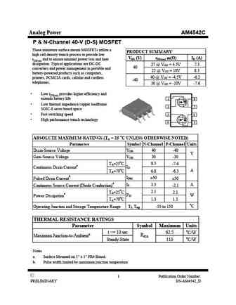
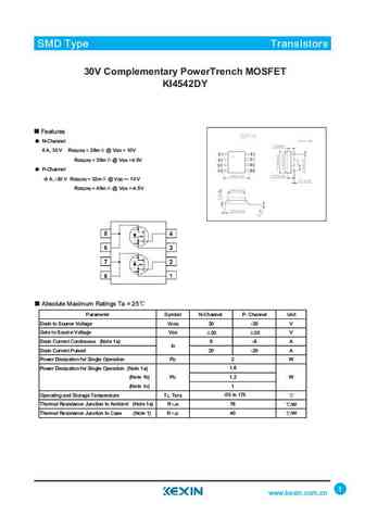
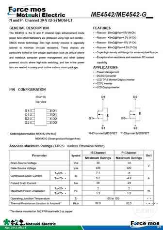
|Vds|ⓘ - Максимально допустимое напряжение сток-исток: 30 V
|Vgs|ⓘ - Максимально допустимое напряжение затвор-исток: 20 V
|Id| ⓘ - Максимально допустимый постоянный ток стока: 6.9 A
Tj ⓘ - Максимальная температура канала: 150 °C
Электрические характеристики
RDSonⓘ - Сопротивление сток-исток открытого транзистора: 0.028 Ohm
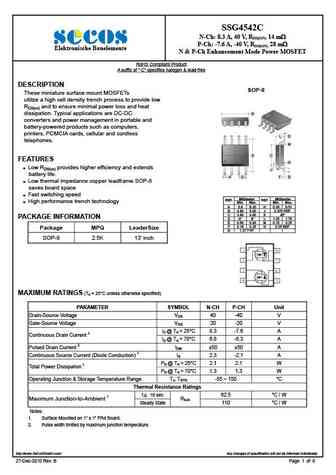
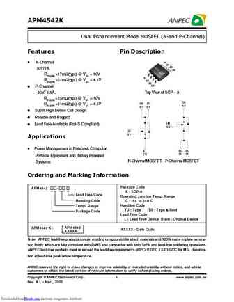
Тип корпуса: SOP8
Аналог (замена) для 4542
- подборⓘ MOSFET транзистора по параметрам
4542 даташит
4542.pdf
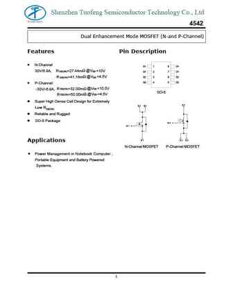
Shenzhen Tuofeng Semiconductor Technology Co., Ltd 4542 Dual Enhancement Mode MOSFET (N-and P-Channel) Features Pin Description N-Channel S1 1 8 D1 30V/6.9A, RDS(ON)=27.44m @VGS =10V G1 2 7 D1 R DS(ON)=41.16m @VGS =4.5V S2 3 6 D2 G2 4 5 D2 P-Channel R DS(ON)=32.00m @VGS =10.0V -30V/-6.9A, SO-8 R DS(ON)=50.00m @VGS =4.5V Super High Dense Ce
si4542dy.pdf
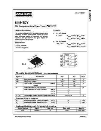
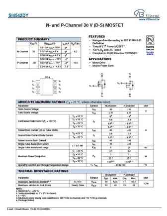
January 2001 Si4542DY 30V Complementary PowerTrench MOSFET General Description Features This complementary MOSFET device is produced using Q1 N-Channel Fairchild s advanced PowerTrench process that has 6 A, 30 V RDS(on) = 28 m @ VGS = 10V been especially tailored to minimize the on-state resistance and yet maintain low gate charge for RDS(on) = 35 m @ VGS
si4542dy.pdf
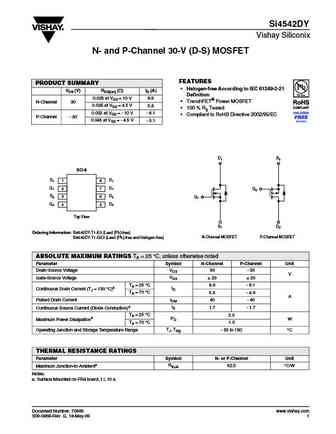
Si4542DY Vishay Siliconix N- and P-Channel 30-V (D-S) MOSFET FEATURES PRODUCT SUMMARY Halogen-free According to IEC 61249-2-21 VDS (V) RDS(on) ( )ID (A) Definition 0.025 at VGS = 10 V 6.9 TrenchFET Power MOSFET N-Channel 30 0.035 at VGS = 4.5 V 5.8 100 % Rg Tested 0.032 at VGS = - 10 V - 6.1 Compliant to RoHS Directive 2002/95/EC P-Channel - 30 0.045
si4542dy.pdf

ON Semiconductor Is Now To learn more about onsemi , please visit our website at www.onsemi.com onsemi and and other names, marks, and brands are registered and/or common law trademarks of Semiconductor Components Industries, LLC dba onsemi or its affiliates and/or subsidiaries in the United States and/or other countries. onsemi owns the rights to a number of patents, trademarks,
Другие MOSFET... 2341 , 4401 , 4402 , 4407 , 4409 , 4410 , 4435 , 4501 , IRF9540N , 4606 , 4611 , 4612 , 4616 , 4622 , 4803 , 4812 , 4835 .
History: J308
History: J308
🌐 : EN ES РУ

Список транзисторов
Обновления
MOSFET: ASD80R750E | ASD70R950E | ASD70R600E | ASD70R380E | ASD65R850E | ASD65R550E | ASD65R350E | ASD65R300E | ASD65R280E | ASD65R270E | ASD60R330E | ASD60R280E | ASB80R750E | ASB70R380E | ASB65R300E | ASB65R220E
Popular searches
2sa726 transistor | 7506 mosfet | irlr8726 datasheet | ru7088r mosfet | mp40 transistor | fgpf4636 datasheet | 2sc1945 | c2383