8810. Аналоги и основные параметры
Наименование производителя: 8810
Тип транзистора: MOSFET
Полярность: N
Предельные значения
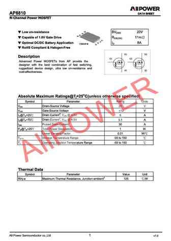
Pd ⓘ - Максимальная рассеиваемая мощность: 1.5 W
|Vds|ⓘ - Максимально допустимое напряжение сток-исток: 20 V
|Vgs|ⓘ - Максимально допустимое напряжение затвор-исток: 8 V
|Id| ⓘ - Максимально допустимый постоянный ток стока: 6 A
Tj ⓘ - Максимальная температура канала: 150 °C
Электрические характеристики
RDSonⓘ - Сопротивление сток-исток открытого транзистора: 0.022 Ohm
Тип корпуса: TSSOP8
Аналог (замена) для 8810
- подборⓘ MOSFET транзистора по параметрам
8810 даташит
8810.pdf
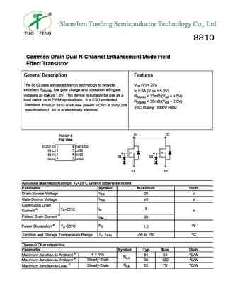
Shenzhen Tuofeng Semiconductor Technology Co., Ltd 8810 Common-Drain Dual N-Channel Enhancement Mode Field Effect Transistor General Description Features The 8810 uses advanced trench technology to provide VDS (V) = 20V excellent RDS(ON), low gate charge and operation with gate ID = 6A (V = 4.5V) GS voltages as low as 1.8V. This device is suitable for use as a RDS(ON)
si8810.pdf
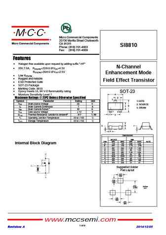
SI8810 Features Low RDS(ON) Rugged and Reliable ESD Protected Gate Lead Free Finish/RoHS Compliant ("P" Suffix Designates RoHS N-Channel MOSFET Compliant. See Ordering Information) Epoxy Meets UL 94 V-0 Flammability Rating Moisture Sensitivity Level 1 Halogen Free Available Upon Request By Adding Suffix "-HF" Maximum Ratings Operating Junction Tempera
cjs8810.pdf
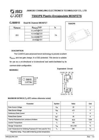
JIANGSU CHANGJING ELECTRONICS TECHNOLOGY CO., LTD TSSOP8 Plastic-Encapsulate MOSFETS CJS8810 Dual N-Channel MOSFET TSSOP8 ID V(BR)DSS RDS(on)TYP @4.5V 14.2m 15.4m @3.8V 20V 7 A 18.2 m @2.5V 26m @1.8V DESCRIPTION The CJS8810 uses advanced trench technology to provide excellent RDS(ON) and low gate charge. It is ESD protected. This device is suitable for use as a uni-
cj8810.pdf
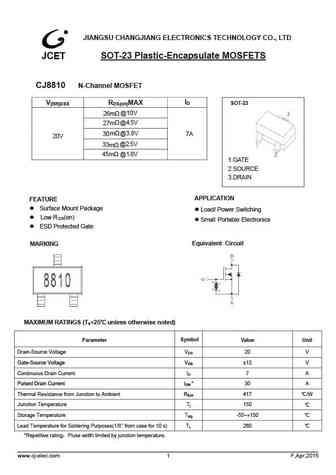
JIANGSU CHANGJIANG ELECTRONICS TECHNOLOGY CO., LTD SOT-23 Plastic-Encapsulate MOSFETS CJ8810 N-Channel MOSFET ID V(BR)DSS RDS(on)MAX SOT-23 V m @10 26 @4.5V 27m m @3.8V 30 7 A 20V @2.5V 33 m 45m @1.8V 1.GATE 2.SOURCE 3.DRAIN APPLICATION FEATURE Surface Mount Package Load/ Power Switching Low R (on) DS Small Portable Electronics
ao8810.pdf
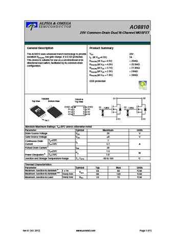
AO8810 20V Common-Drain Dual N-Channel MOSFET General Description Product Summary VDS 20V The AO8810 uses advanced trench technology to provide excellent RDS(ON), low gate charge. It is ESD protected. ID (at VGS=4.5V) 7A This device is suitable for use as a uni-directional or bi- RDS(ON) (at VGS= 4.5V)
mtdn8810at8.pdf
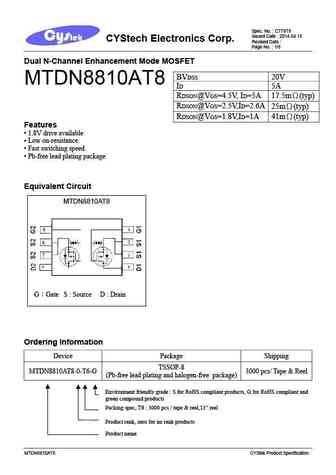
Spec. No. C779T8 Issued Date 2014.04.15 CYStech Electronics Corp. Revised Date Page No. 1/8 Dual N-Channel Enhancement Mode MOSFET BVDSS 20V MTDN8810AT8 ID 5A RDSON@VGS=4.5V, ID=5A 17.5m (typ) RDSON@VGS=2.5V,ID=2.6A 25m (typ) RDSON@VGS=1.8V,ID=1A 41m (typ) Features 1.8V drive available Low on-resistance Fast switching speed Pb-free lead pl
mtdn8810t8.pdf
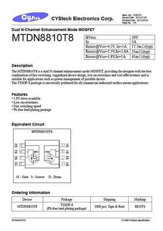
Spec. No. C582T8 Issued Date 2013.07.25 CYStech Electronics Corp. Revised Date 2013.09.03 Page No. 1/8 Dual N-Channel Enhancement Mode MOSFET BVDSS 20V MTDN8810T8 ID 5A RDSON@VGS=4.5V, ID=5A 17.5m (typ) RDSON@VGS=2.5V,ID=2.6A 25m (typ) RDSON@VGS=1.8V,ID=1A 41m (typ) Description The MTDN8810T8 is a dual N-channel enhancement-mode MOSFET, providing the designer w
stf8810.pdf
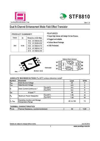
Green Product STF8810 a S mHop Microelectronics C orp. Ver 1.3 Dual N-Channel Enhancement Mode Field Effect Transistor FEATURES PRODUCT SUMMARY Super high dense cell design for low RDS(ON). VDSS ID RDS(ON) (m ) Max Rugged and reliable. 16.0 @ VGS=4.5V Suface Mount Package. 17.0 @ VGS=4.0V 20V 8.0A 18.0 @ VGS=3.7V ESD Protected. 21.0 @ VGS=3.1V 27.5 @ VGS=2.5V G2 Bottom Drain
stg8810.pdf
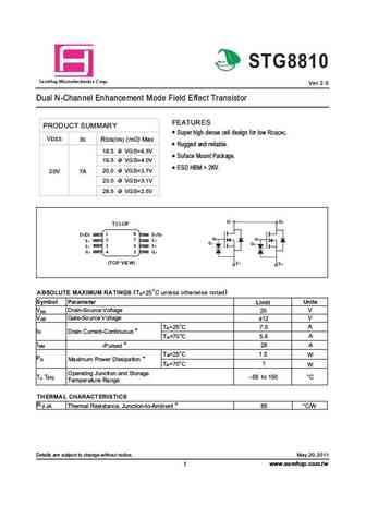
Gr P Pr P P STG8810 a S mHop Microelectronics C orp. Ver 2.0 Dual N-Channel Enhancement Mode Field Effect Transistor FEATURES PRODUCT SUMMARY Super high dense cell design for low RDS(ON). VDSS ID RDS(ON) (m ) Max Rugged and reliable. 18.5 @ VGS=4.5V Suface Mount Package. 19.5 @ VGS=4.0V ESD HBM > 2KV. 20V 7A 20.0 @ VGS=3.7V 23.0 @ VGS=3.1V 28.5 @ VGS=2.5V D1 D2 TS S OP
stg8810a.pdf
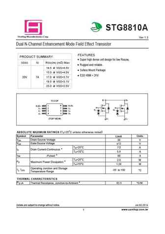
Green Product STG8810A a S mHop Microelectronics C orp. Ver 1.3 Dual N-Channel Enhancement Mode Field Effect Transistor FEATURES PRODUCT SUMMARY Super high dense cell design for low RDS(ON). VDSS ID RDS(ON) (m ) Max Rugged and reliable. 14.5 @ VGS=4.5V Suface Mount Package. 15.0 @ VGS=4.0V ESD HBM > 2KV. 20V 7A 17.0 @ VGS=3.7V 19.5 @ VGS=3.1V 23.0 @ VGS=2.5V D1 D2 TS S
ssf8810.pdf
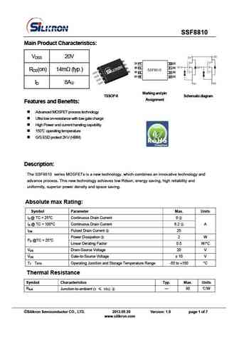
SSF8810 Main Product Characteristics VDSS 20V RDS(on) 14m (typ.) ID 8A Marking and pin TSSOP-8 Schematic diagram Assignment Features and Benefits Advanced MOSFET process technology Ultra low on-resistance with low gate charge High Power and current handing capability 150 operating temperature G/S ESD protect 2KV (HBM) Description Th
br8810mf.pdf
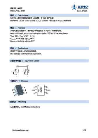
BR8810MF Rev.E Oct.-2017 DATA SHEET / Descriptions SOT23-6 N MOS ESD N-channel Double MOSFET in a SOT23-6 Plastic Package. It is ESD protested. / Features RDS(on) advanced trench technology to provide excellent RDS(on), low gate charge. VD
ftk8810l.pdf
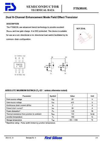
SEMICONDUCTOR FTK8810L TECHNICAL DATA Dual N-Channel Enhancement Mode Field Effect Transistor DESCRIPTION The FTK8810L use advanced trench technology to provide excellent SOT-23-6L RDS(ON) and low gate charge. It is ESD protected. This device is suitable for use as a uni-directional or bi-directional load switch,facilitated by its common-drain configuration. ABSOLUTE MAXIMUM RAT
ftk8810.pdf
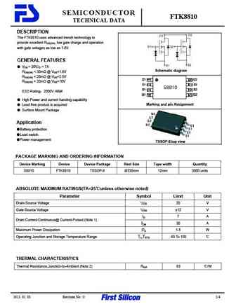
SEMICONDUCTOR FTK8810 TECHNICAL DATA DESCRIPTION The FTK8810 uses advanced trench technology to provide excellent RDS(ON), low gate charge and operation with gate voltages as low as 1.8V. GENERAL FEATURES VDS = 20V,ID = 7A Schematic diagram RDS(ON)
ao8810.pdf
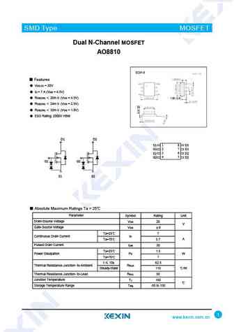
SMD Type MOSFET Dual N-Channel MOSFET AO8810 SOP-8 Features VDS (V) = 20V ID = 7 A (VGS = 4.5V) RDS(ON) 20m (VGS = 4.5V) 1.50 0.15 RDS(ON) 24m (VGS = 2.5V) RDS(ON) 32m (VGS = 1.8V) ESD Rating 2000V HBM D1 D2 S1 1 8 D1 2 7 G1 D1 3 6 S2 D2 4 5 G2 D2 G1 G2 S2 S1 Absolute Maximum Ratings Ta = 25 Parameter Symbol Rati
ki8810dy.pdf
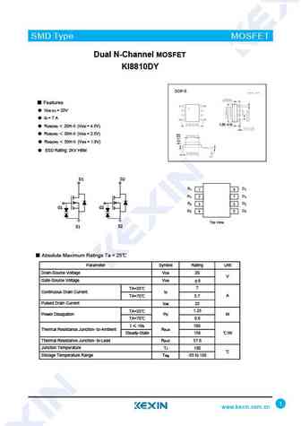
SMD Type MOSFET Dual N-Channel MOSFET KI8810DY SOP-8 Features VDS (V) = 20V ID = 7 A 1.50 0.15 RDS(ON) 20m (VGS = 4.5V) RDS(ON) 30m (VGS = 2.5V) RDS(ON) 50m (VGS = 1.8V) ESD Rating 2KV HBM D1 D2 S1 1 D1 8 G1 2 D1 7 S2 3 D2 6 G1 G2 G2 4 D2 5 Top View S2 S1 Absolute Maximum Ratings Ta = 25 Parameter Symbol Ratin
ki8810t.pdf
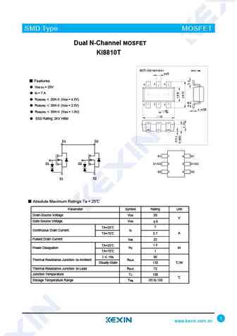
SMD Type MOSFET Dual N-Channel MOSFET KI8810T ( ) SOT-23-6 Unit mm 0.4+0.1 -0.1 Features 6 5 4 VDS (V) = 20V ID = 7 A RDS(ON) 20m (VGS = 4.5V) 2 3 1 RDS(ON) 30m (VGS = 2.5V) +0.02 0.15 -0.02 +0.01 -0.01 RDS(ON) 50m (VGS = 1.8V) +0.2 -0.1 ESD Rating 2KV HBM D1 D2 S1 1 6 G1 G1 G2 D1/D2 2 5 D1/D2 S2 3 4 G2 S2 S1
ki8810ds.pdf
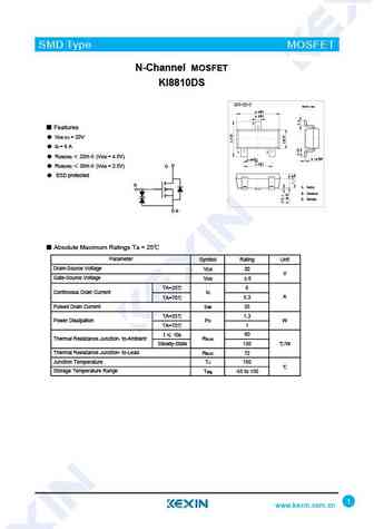
SMD Type MOSFET N-Channel MOSFET KI8810DS SOT-23-3 Unit mm +0.2 2.9 -0.1 +0.1 0.4-0.1 3 Features VDS (V) = 20V ID = 6 A 1 2 RDS(ON) 22m (VGS = 4.5V) +0.02 +0.1 0.15 -0.02 0.95 -0.1 +0.1 1.9 -0.2 RDS(ON) 30m (VGS = 2.5V) D ESD protected G 1. Gate 2. Source 3. Drain S Absolute Maximum Ratings Ta = 25 Parameter Symbol R
am8810.pdf
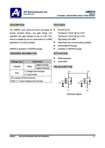
AiT Semiconductor Inc. AM8810 www.ait-ic.com MOSFET N-CHANNEL ENHANCEMENT MODE POWER MOSFET DESCRIPTION FEATURES The AM8810 uses advanced trench technology to V =20V,I =7A, DS D provide excellent R , low gate charge and Typ.R = 16m @ V =4.5V DS(ON) DS(ON) GS operation with gate voltages as low as 2.5V. This Typ.R = 20m @ V =2.5V DS(ON) GS device is suitable for use as
elm18810ba.pdf
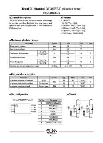
(common drain) Dual N-channel MOSFET ELM18810BA-S General description Features ELM18810BA-S uses advanced trench technology Vds=20V to provide excellent Rds(on), low gate charge and Id=7A (Vgs=4.5V) operation with gate voltages as low as 1.8V and internal Rds(on)
smc8810a.pdf
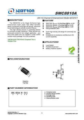
SMC8810A 20V N-Channel Enhancement Mode MOSFET DESCRIPTION FEATURE The SMC8810A is the Single N-Channel logic 20V/7.0A, RDS(ON) =14.5m (typ.)@VGS =4.5V enhancement mode power field effect transistor 20V/6.5A, RDS(ON) =17m (typ.)@VGS =2.5V which is produced using high cell density. advanced 20V/5.0A, RDS(ON) =27m (typ.)@VGS =1.8V trench technology to prov
smc8810.pdf
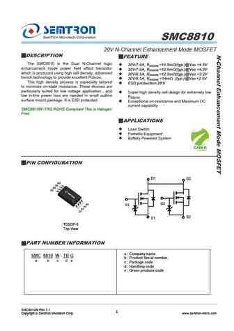
SMC8810 20V N-Channel Enhancement Mode MOSFET DESCRIPTION FEATURE The SMC8810 is the Dual N-Channel logic 20V/7.0A, RDS(ON) =11.5m (typ.)@VGS =4.5V enhancement mode power field effect transistor 20V/7.0A, RDS(ON) =12.0m (typ.)@VGS =4.0V which is produced using high cell density. advanced 20V/6.5A, RDS(ON) =12.5m (typ.)@VGS =3.2V trench technology to prov
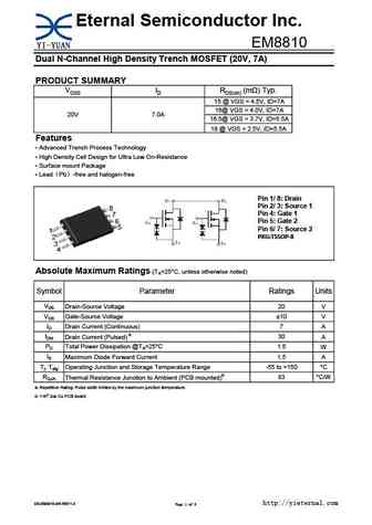
hso8810.pdf
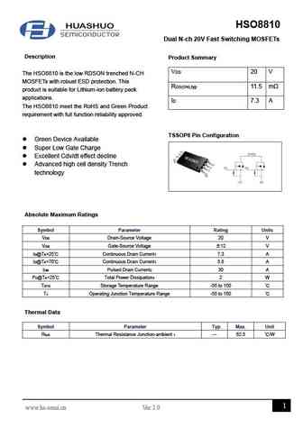
HSO8810 Dual N-ch 20V Fast Switching MOSFETs Description Product Summary VDS 20 V The HSO8810 is the low RDSON trenched N-CH MOSFETs with robust ESD protection. This RDS(ON),typ 11.5 m product is suitable for Lithium-ion battery pack applications. ID 7.3 A The HSO8810 meet the RoHS and Green Product requirement with full function reliability approved. TSSOP8 Pin Conf
hsw8810.pdf
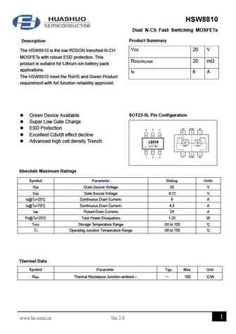
HSW8810 Dual N-Ch Fast Switching MOSFETs Description Product Summary VDS 20 V The HSW8810 is the low RDSON trenched N-CH MOSFETs with robust ESD protection. This RDS(ON),max 20 m product is suitable for Lithium-ion battery pack applications. ID 6 A The HSW8810 meet the RoHS and Green Product requirement with full function reliability approved. Green Device Availabl
jmtt8810ks.pdf
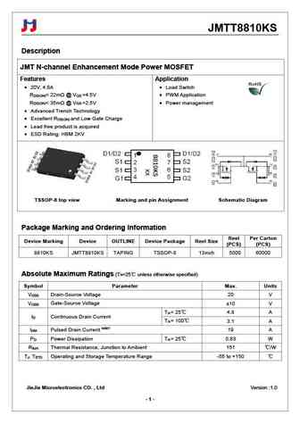
JMTT8810KS Description JMT N-channel Enhancement Mode Power MOSFET Features Application 20V, 4.8A Load Switch R
jmtm8810ks.pdf
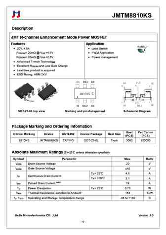
JMTM8810KS Description JMT N-channel Enhancement Mode Power MOSFET Features Application 20V, 4.8A Load Switch R
pt8810.pdf
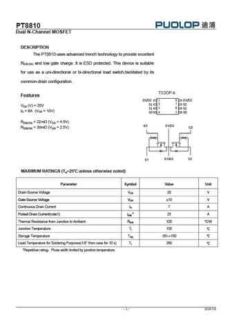
PT8810 Dual N-Channel MOSFET DESCRIPTION The PT8810 uses advanced trench technology to provide excellent RDS(ON) and low gate charge. It is ESD protected. This device is suitable for use as a uni-directional or bi-directional load switch,facilitated by its common-drain configuration. TSSOP-8 Features D1/D2 1 8 D1/D2 2 7 S1 S2 VDS (V) = 20V 3 6 S1 S2 ID = 6A (VGS = 10V) 4 5
8810b.pdf
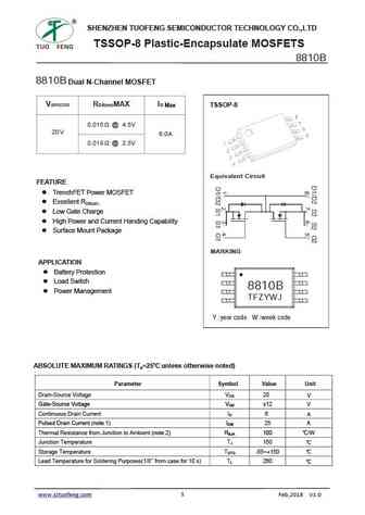
SHENZHEN TUOFENG SEMICONDUCTOR TECHNOLOGY CO.,LTD TSSOP-8 Plastic-Encapsulate MOSFETS 8810B 8810B Dual N-Channel MOSFET V(BR)DSS RDS(on)MAX ID TSSOP-8 Max 0.015 @ 4.5V 20V 6.0A 0.019 @ 2.5V Equivalent Circuit FEATURE TrenchFET Power MOSFET Excellent RDS(on) Low Gate Charge High Power and Current Handing Capability Surface Mount Package MARKING APPLICAT
wsp8810.pdf
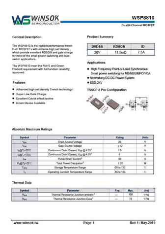
WSP8810 Dual N-Channel MOSFET Product Summery General Description The WSP8810 is the highest performance trench BVDSS RDSON ID N-ch MOSFETs with extreme high cell density , which provide excellent RDSON and gate charge 20V 11.5m 7.5A for most of the small power switching and load switch applications. Applications The WSP8810 meet the RoHS and Green Product requirement w
wsp8810a.pdf
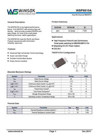
WSP8810A Dual N-Channel MOSFET Product Summery General Description The WSP8810A is the highest performance BVDSS RDSON ID trench N-ch MOSFET with extreme high cell 20V 14.5m 7.0A density , which provide excellent RDSON and gate charge for most of the small power switching and load switch applications. Applications The WSP8810A meet the RoHS and Green High Frequency Po
se8810.pdf
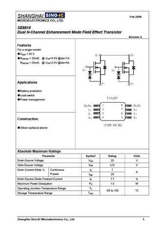
SHANGHAI Feb 2008 MICROELECTRONICS CO., LTD. SE8810 Dual N-Channel Enhancement Mode Field Effect Transistor Revision A Features For a single mosfet VDSS = 20 V RDS(ON)
se8810a.pdf
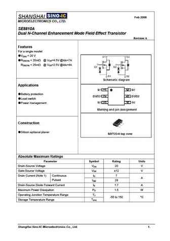
SHANGHAI Feb 2008 MICROELECTRONICS CO., LTD. SE8810A Dual N-Channel Enhancement Mode Field Effect Transistor Revision A Features For a single mosfet VDSS = 20 V RDS(ON)
ao8810.pdf
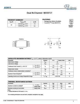
AO8810 www.VBsemi.tw Dual N-Channel MOSFET FEATURES PRODUCT SUMMARY Halogen-free Option Available VDS (V) RDS(on) ( )ID (A) Pb-free TrenchFET Power MOSFETs 0.013 at VGS = 4.5 V Available 7.6 20 RoHS* 0.020 at VGS = 2.5 V 6.5 COMPLIANT D D TSSOP-8 D D 1 8 S S 1 2 7 2 S S G1 G2 1 3 6 2 G 1 4 G 2 5 S1 S2 Top View ABSOLUTE MAXIMUM RATINGS TA = 25
hm8810e.pdf
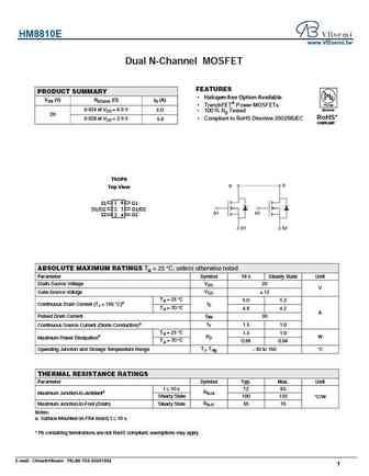
HM8810E www.VBsemi.tw Dual N-Channel MOSFET FEATURES PRODUCT SUMMARY Halogen-free Option Available VDS (V) RDS(on) ( )ID (A) Pb-free TrenchFET Power MOSFETs 0.024 at VGS = 4.5 V Available 6.0 100 % Rg Tested 20 RoHS* 0.028 at VGS = 2.5 V Compliant to RoHS Directive 2002/95/EC 5.0 COMPLIANT TSOP6 D D Top View S1 1 6 G1 D1/D2 2 5 D1/D2 G1 G2 S2 G2 3 4
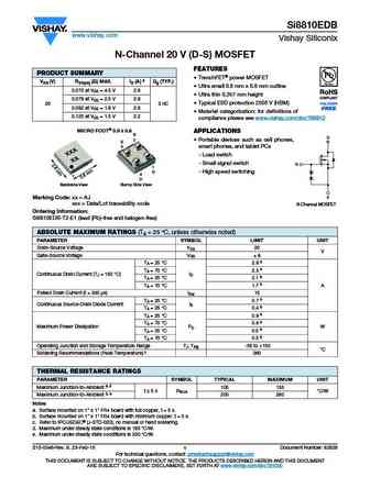
vbzc8810.pdf
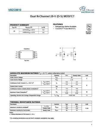
VBZC8810 www.VBsemi.com Dual N-Channel 20-V (D-S) MOSFET FEATURES PRODUCT SUMMARY Halogen-free Option Available VDS (V) RDS(on) ( )ID (A) Pb-free TrenchFET Power MOSFETs 0.018 at VGS = 4.5 V Available 5.0 20 RoHS* 0.030 at VGS = 2.5 V 3.6 COMPLIANT D D TSSOP-8 D D 1 8 S S 1 2 7 2 S S G1 G2 1 3 6 2 G 1 4 G 2 5 S1 S2 Top View ABSOLUTE MAXIMUM RAT
hm8810s.pdf
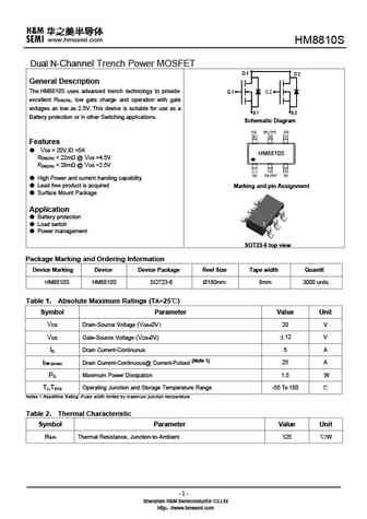
HM8810S Dual N-Channel Trench Power MOSFET General Description The HM8810S uses advanced trench technology to provide excellent R , low gate charge and operation with gate DS(ON) voltages as low as 2.5V. This device is suitable for use as a Battery protection or in other Switching applications. Schematic Diagram Features VDS = 20V,ID =5A HM8810S R
hm8810a.pdf
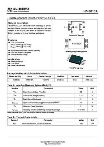
HM Dual N-Channel Trench Power MOSFET General Description The HM uses advanced trench technology to provide excellent R , low gate charge and operation with gate DS(ON) voltages as low as 2.5V. This device is suitable for use as a Battery protection or in other Switching applications. Schematic Diagram Features VDS = 20V,ID =7A HM R
hm8810e.pdf
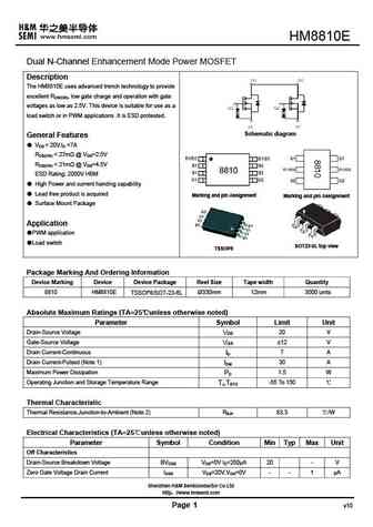
HM8810E Dual N-Channel Enhancement Mode Power MOSFET Description The HM8810E uses advanced trench technology to provide excellent RDS(ON), low gate charge and operation with gate voltages as low as 2.5V. This device is suitable for use as a load switch or in PWM applications .It is ESD protested. Schematic diagram General Features VDS = 20V,ID =7A RDS(ON)
Другие MOSFET... 4622 , 4803 , 4812 , 4835 , 4920 , 4946 , 4953 , 6604 , 5N65 , 8820 , 8822 , 9435 , 4953A , 4953B , 9926A , 9926B , AO3410 .
🌐 : EN ES РУ

Список транзисторов
Обновления
MOSFET: ASD80R750E | ASD70R950E | ASD70R600E | ASD70R380E | ASD65R850E | ASD65R550E | ASD65R350E | ASD65R300E | ASD65R280E | ASD65R270E | ASD60R330E | ASD60R280E | ASB80R750E | ASB70R380E | ASB65R300E | ASB65R220E
Popular searches
jcs640c | kn2907a | ncep028n85 datasheet | sw50n06 | 2sa1232 | 2sc1940 | ftp08n06a | 2n3405