20N06. Аналоги и основные параметры
Наименование производителя: 20N06
Тип транзистора: MOSFET
Полярность: N
Предельные значения
Pd ⓘ - Максимальная рассеиваемая мощность: 40 W
|Vds|ⓘ - Максимально допустимое напряжение сток-исток: 60 V
|Vgs|ⓘ - Максимально допустимое напряжение затвор-исток: 20 V
|Id| ⓘ - Максимально допустимый постоянный ток стока: 20 A
Tj ⓘ - Максимальная температура канала: 175 °C
Электрические характеристики
RDSonⓘ - Сопротивление сток-исток открытого транзистора: 0.045 Ohm
Тип корпуса: TO252
Аналог (замена) для 20N06
- подборⓘ MOSFET транзистора по параметрам
20N06 даташит
20n06.pdf
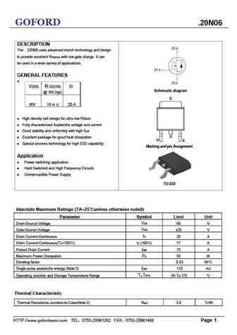
GOFORD .20N06 DESCRIPTION The . 2 0N06 uses advanced trench technology and design to provide excellent RDS(ON) with low gate charge. It can be used in a wide variety of applications. GENERAL FEATURES VDSS R DS(ON) ID Schematic diagram @ 10V (typ) 60V 18 m 25 A High density cell design for ultra low Rdson Fully characterized Avalanche voltage and current
20n06.pdf
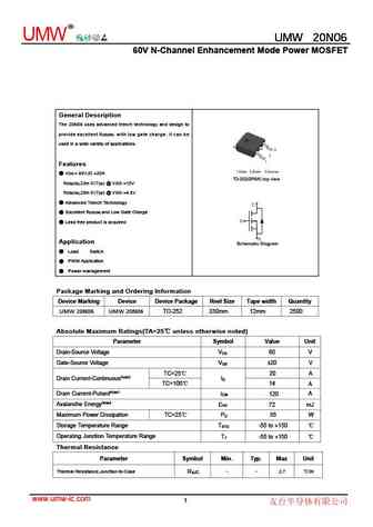
R UMW UMW 20N06 UMW 20N06 60V N-Channel Enhancement Mode Power MOSFET General Description The 20N06 uses advanced trench technology and design to provide excellent RDS(ON) with low gate charge. It can be used in a wide variety of applications. Features VDS = 60V,ID =20A RDS(ON),23m (Typ) @ VGS =10V RDS(ON),29m (Typ) @ VGS =4.5V Advanced Trench Technology Excellent RDS(ON) and Lo
20n06.pdf
20N06 20N06 60V N-Channel Enhancement Mode Power MOSFET General Description The 20N06 uses advanced trench technology and design to provide excellent RDS(ON) with low gate charge. It can be used in a wide variety of applications. Features VDS = 60V,ID =20A RDS(ON),23m (Typ) @ VGS =10V RDS(ON),29m (Typ) @ VGS =4.5V Advanced Trench Technology Excellent RDS(ON) and Low Gate Charge
20n06.pdf
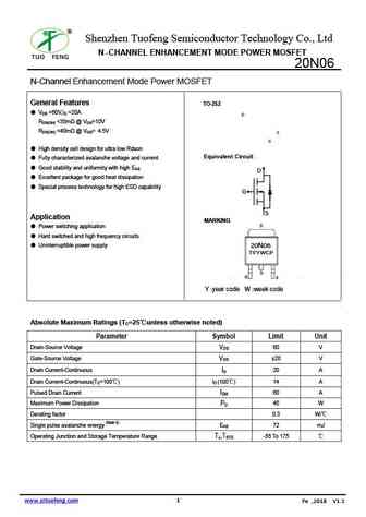
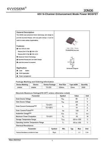
Shenzhen Tuofeng Semiconductor Technology Co., Ltd N -CHANNEL ENHANCEMENT MODE POWER MOSFET 20N06 Enhancement Mode Power MOSFET N-Channel General Features TO-252 VDS =60V,ID =20A D RDS(ON)
20n06.pdf
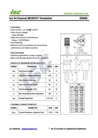
INCHANGE Semiconductor isc N-Channel MOSFET Transistor 20N06 FEATURES Drain Current I = 20A@ T =25 D C Drain Source Voltage- V = 60V(Min) DSS Static Drain-Source On-Resistance R = 0.085 (Max) DS(on) Fast Switching Minimum Lot-to-Lot variations for robust device performance and reliable operation APPLICATIONS Switching applications in power supplies Moto
mtd20n06v.pdf

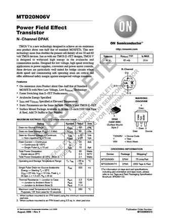
MOTOROLA Order this document SEMICONDUCTOR TECHNICAL DATA by MTD20N06V/D Designer's Data Sheet MTD20N06V TMOS V Power Field Effect Transistor DPAK for Surface Mount TMOS POWER FET N Channel Enhancement Mode Silicon Gate 20 AMPERES 60 VOLTS TMOS V is a new technology designed to achieve an on resis- RDS(on) = 0.080 OHM tance area product about one half that of standa
mtp20n06v.pdf
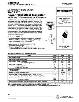
MOTOROLA Order this document SEMICONDUCTOR TECHNICAL DATA by MTP20N06V/D Designer's Data Sheet MTP20N06V TMOS V Power Field Effect Transistor N Channel Enhancement Mode Silicon Gate TMOS POWER FET TMOS V is a new technology designed to achieve an on resis- 20 AMPERES tance area product about one half that of standard MOSFETs. This 60 VOLTS new technology more than
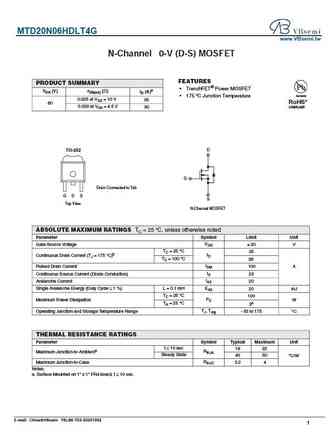
mtd20n06hdl.pdf
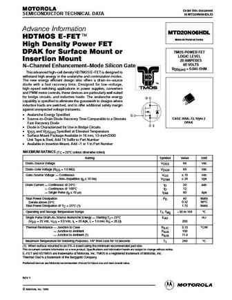
MOTOROLA Order this document SEMICONDUCTOR TECHNICAL DATA bt MTD20N06HDL/D Advance Information MTD20N06HDL HDTMOS E-FET Motorola Preferred Device High Density Power FET TMOS POWER FET DPAK for Surface Mount or LOGIC LEVEL Insertion Mount 20 AMPERES 60 VOLTS N Channel Enhancement Mode Silicon Gate RDS(on) = 0.045 OHM This advanced high cell density HDTMOS E FET is de
mtd20n06hd.pdf

MOTOROLA Order this document SEMICONDUCTOR TECHNICAL DATA bt MTD20N06HDL/D Advance Information MTD20N06HDL HDTMOS E-FET Motorola Preferred Device High Density Power FET TMOS POWER FET DPAK for Surface Mount or LOGIC LEVEL Insertion Mount 20 AMPERES 60 VOLTS N Channel Enhancement Mode Silicon Gate RDS(on) = 0.045 OHM This advanced high cell density HDTMOS E FET is de
mtd20n06h.pdf
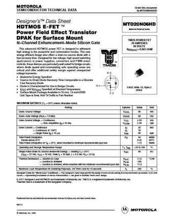
MOTOROLA Order this document SEMICONDUCTOR TECHNICAL DATA by MTD20N06HD/D Designer's Data Sheet MTD20N06HD HDTMOS E-FET. Motorola Preferred Device Power Field Effect Transistor DPAK for Surface Mount TMOS POWER FET 20 AMPERES N Channel Enhancement Mode Silicon Gate 60 VOLTS This advanced HDTMOS power FET is designed to withstand RDS(on) = 0.045 OHM high energy in the
mtd20n06vrev1.pdf

MOTOROLA Order this document SEMICONDUCTOR TECHNICAL DATA by MTD20N06V/D Designer's Data Sheet MTD20N06V TMOS V Power Field Effect Transistor DPAK for Surface Mount TMOS POWER FET N Channel Enhancement Mode Silicon Gate 20 AMPERES 60 VOLTS TMOS V is a new technology designed to achieve an on resis- RDS(on) = 0.080 OHM tance area product about one half that of standa
phx20n06t.pdf
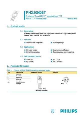
PHX20N06T N-channel TrenchMOS standard level FET Rev. 01 16 February 2004 Product data M3D308 1. Product profile 1.1 Description N-channel enhancement mode field-effect power transistor in a fully isolated plastic package using TrenchMOS technology. 1.2 Features Standard level compatible Isolated package. 1.3 Applications DC motor control Synchronous rectification DC-to
php20n06t phb20n06t.pdf
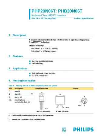
PHP20N06T; PHB20N06T N-channel TrenchMOS transistor Rev. 01 22 February 2001 Product specification 1. Description N-channel enhancement mode field-effect transistor in a plastic package using TrenchMOS 1 technology. Product availability PHP20N06T in SOT78 (TO-220AB) PHB20N06T in SOT404 (D 2-PAK). 2. Features Very low on-state resistance Fast switching. 3. Applications
php20n06e 1.pdf
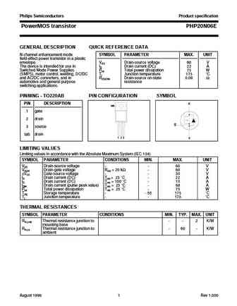
Philips Semiconductors Product specification PowerMOS transistor PHP20N06E GENERAL DESCRIPTION QUICK REFERENCE DATA N-channel enhancement mode SYMBOL PARAMETER MAX. UNIT field-effect power transistor in a plastic envelope. VDS Drain-source voltage 60 V The device is intended for use in ID Drain current (DC) 22 A Switched Mode Power Supplies Ptot Total power dissipation 75 W (SMPS), mo
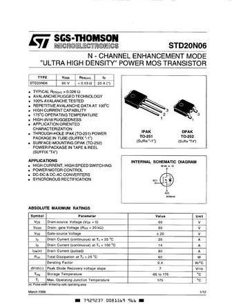
stp20n06.pdf

STP20N06 STP20N06FI N - CHANNEL ENHANCEMENT MODE POWER MOS TRANSISTOR TYPE VDSS RDS(on) ID STP20N06 60 V
stp20n06-fi.pdf
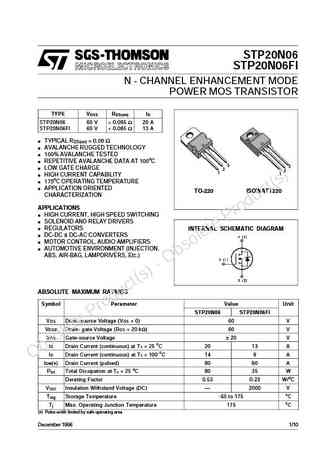
STP20N06 STP20N06FI N - CHANNEL ENHANCEMENT MODE POWER MOS TRANSISTOR TYPE VDSS RDS(on) ID STP20N06 60 V
fqp20n06tstu.pdf
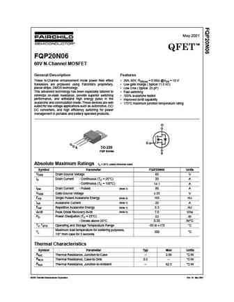
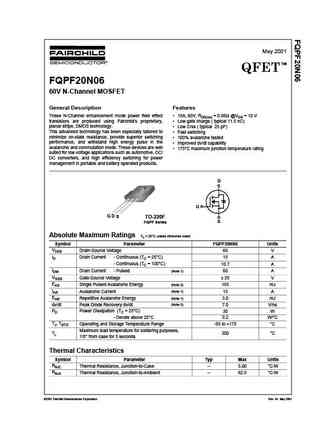
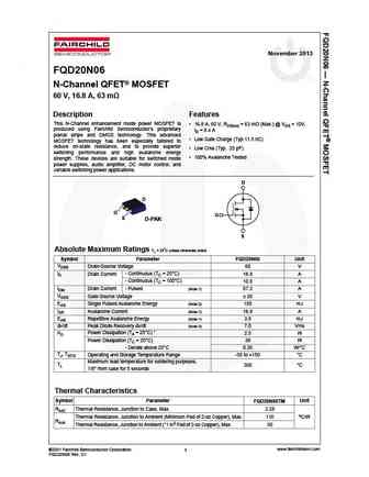
May 2001 TM QFET FQP20N06 60V N-Channel MOSFET General Description Features These N-Channel enhancement mode power field effect 20A, 60V, RDS(on) = 0.06 @VGS = 10 V transistors are produced using Fairchild s proprietary, Low gate charge ( typical 11.5 nC) planar stripe, DMOS technology. Low Crss ( typical 25 pF) This advanced technology has been especially tailored to
fqp20n06l.pdf
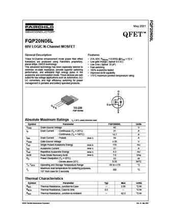
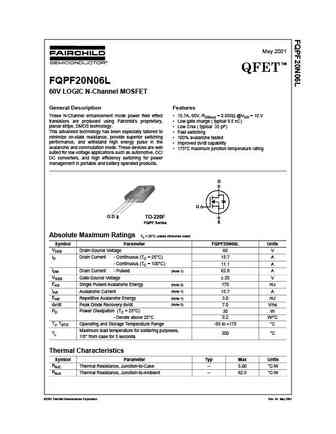
May 2001 TM QFET FQP20N06L 60V LOGIC N-Channel MOSFET General Description Features These N-Channel enhancement mode power field effect 21A, 60V, RDS(on) = 0.055 @VGS = 10 V transistors are produced using Fairchild s proprietary, Low gate charge ( typical 9.5 nC) planar stripe, DMOS technology. Low Crss ( typical 35 pF) This advanced technology has been especially tail
fqp20n06.pdf

May 2001 TM QFET FQP20N06 60V N-Channel MOSFET General Description Features These N-Channel enhancement mode power field effect 20A, 60V, RDS(on) = 0.06 @VGS = 10 V transistors are produced using Fairchild s proprietary, Low gate charge ( typical 11.5 nC) planar stripe, DMOS technology. Low Crss ( typical 25 pF) This advanced technology has been especially tailored to
fqd20n06tf fqd20n06tm fqd20n06 fqu20n06 fqu20n06tu.pdf
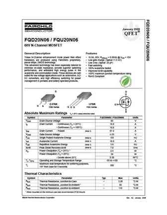
January 2009 QFET FQD20N06 / FQU20N06 60V N-Channel MOSFET General Description Features These N-Channel enhancement mode power field effect 16.8A, 60V, RDS(on) = 0.063 @ VGS = 10V transistors are produced using Fairchild s proprietary, Low gate charge ( typical 11.5 nC) planar stripe, DMOS technology. Low Crss ( typical 25 pF) This advanced technology has been especi
fqd20n06l fqu20n06l.pdf

May 2001 TM QFET FQD20N06L / FQU20N06L 60V LOGIC N-Channel MOSFET General Description Features These N-Channel enhancement mode power field effect 17.2A, 60V, RDS(on) = 0.06 @ VGS = 10V transistors are produced using Fairchild s proprietary, Low gate charge ( typical 9.5 nC) planar stripe, DMOS technology. Low Crss ( typical 35 pF) This advanced technology has been es
fqb20n06ltm.pdf
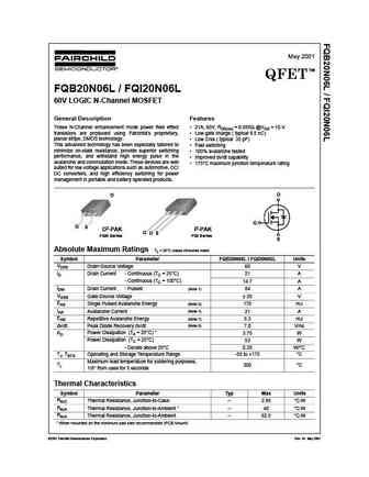
May 2001 TM QFET FQB20N06L / FQI20N06L 60V LOGIC N-Channel MOSFET General Description Features These N-Channel enhancement mode power field effect 21A, 60V, RDS(on) = 0.055 @VGS = 10 V transistors are produced using Fairchild s proprietary, Low gate charge ( typical 9.5 nC) planar stripe, DMOS technology. Low Crss ( typical 35 pF) This advanced technology has been esp
fqd20n06l.pdf
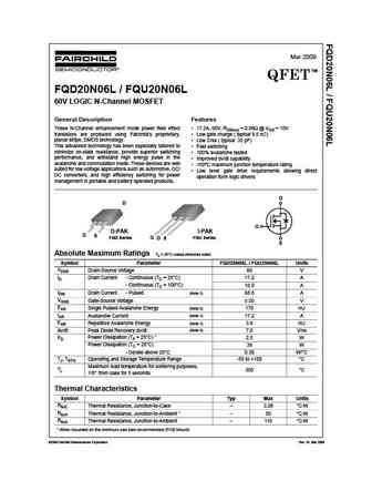
Mar 2009 TM QFET FQD20N06L / FQU20N06L 60V LOGIC N-Channel MOSFET General Description Features These N-Channel enhancement mode power field effect 17.2A, 60V, RDS(on) = 0.06 @ VGS = 10V transistors are produced using Fairchild s proprietary, Low gate charge ( typical 9.5 nC) planar stripe, DMOS technology. Low Crss ( typical 35 pF) This advanced technology has been es
fdp020n06b f102.pdf
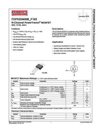
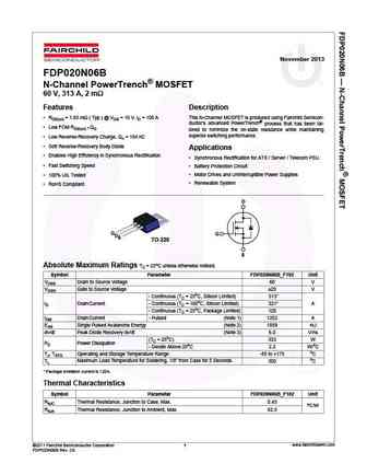
January 2012 FDP020N06B_F102 N-Channel PowerTrench MOSFET 60V, 313A, 2m Features Description RDS(on) = 1.65m ( Typ.) at VGS = 10V, ID = 100A This N-Channel MOSFET is produced using Fairchild Semicon- ductor s advanced PowerTrench process that has been tailored Low FOM RDS(on) *QG to minimize the on-state resistance while maintaining superior switching performance
fqb20n06tm.pdf
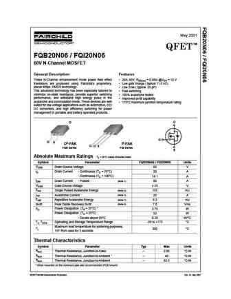
May 2001 TM QFET FQB20N06 / FQI20N06 60V N-Channel MOSFET General Description Features These N-Channel enhancement mode power field effect 20A, 60V, RDS(on) = 0.06 @VGS = 10 V transistors are produced using Fairchild s proprietary, Low gate charge ( typical 11.5 nC) planar stripe, DMOS technology. Low Crss ( typical 25 pF) This advanced technology has been especially
fqpf20n06.pdf
May 2001 TM QFET FQPF20N06 60V N-Channel MOSFET General Description Features These N-Channel enhancement mode power field effect 15A, 60V, RDS(on) = 0.06 @VGS = 10 V transistors are produced using Fairchild s proprietary, Low gate charge ( typical 11.5 nC) planar stripe, DMOS technology. Low Crss ( typical 25 pF) This advanced technology has been especially tailored t
fqpf20n06l.pdf
May 2001 TM QFET FQPF20N06L 60V LOGIC N-Channel MOSFET General Description Features These N-Channel enhancement mode power field effect 15.7A, 60V, RDS(on) = 0.055 @VGS = 10 V transistors are produced using Fairchild s proprietary, Low gate charge ( typical 9.5 nC) planar stripe, DMOS technology. Low Crss ( typical 35 pF) This advanced technology has been especially t
fdp020n06b.pdf
November 2013 FDP020N06B N-Channel PowerTrench MOSFET 60 V, 313 A, 2 m Features Description RDS(on) = 1.65 m ( Typ.) @ VGS = 10 V, ID = 100 A This N-Channel MOSFET is produced using Fairchild Semicon- ductor s advanced PowerTrench process that has been tai- Low FOM RDS(on) * QG lored to minimize the on-state resistance while maintaining superior switching performance.
fdpf320n06l.pdf
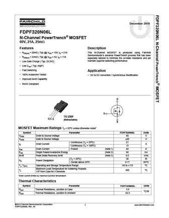
December 2010 FDPF320N06L N-Channel PowerTrench MOSFET 60V, 21A, 25m Features Description RDS(on) = 20m ( Typ.)@ VGS = 10V, ID = 21A This N-Channel MOSFET is produced using Fairchild Semiconductor s advance PowerTrench process that has been RDS(on) = 23m ( Typ.)@ VGS = 5V, ID = 17A especially tailored to minimize the on-state resistance and yet maintain superior sw
phd20n06t.pdf
PHD20N06T N-channel TrenchMOS standard level FET Rev. 02 1 December 2009 Product data sheet 1. Product profile 1.1 General description Standard level N-channel enhancement mode Field-Effect Transistor (FET) in a plastic package using TrenchMOS technology. This product is designed and qualified for use in computing, communications, consumer and industrial applications only. 1.2 Fea
phb20n06t.pdf
PHB20N06T N-channel TrenchMOS standard level FET Rev. 02 25 November 2009 Product data sheet 1. Product profile 1.1 General description Standard level N-channel enhancement mode Field-Effect Transistor (FET) in a plastic package using TrenchMOS technology. This product is designed and qualified for use in computing, communications, consumer and industrial applications only. 1.2 Fe
php20n06t.pdf
PHP20N06T N-channel TrenchMOS standard level FET Rev. 02 27 November 2009 Product data sheet 1. Product profile 1.1 General description Standard level N-channel enhancement mode Field-Effect Transistor (FET) in a plastic package using TrenchMOS technology. This product is designed and qualified for use in computing, communications, consumer and industrial applications only. 1.2 Fe
rhp020n06.pdf
4V Drive Nch MOSFET RHP020N06 Structure Dimensions (Unit mm) Silicon N-channel MOSFET MPT3 4.5 1.5 1.6 Features 1) Low On-resistance. (1) (2) (3) 2) High speed switching. 0.4 3) Wide SOA. 0.5 0.4 0.4 1.5 1.5 3.0 (1)Gate (2)Drain (3)Source Abbreviated symbol LR Applications Switching Packaging specifications and hFE Inner circuit DRAIN Package Taping
rsr020n06tl.pdf
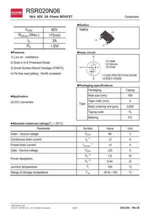
RSR020N06 Nch 60V 2A Power MOSFET Datasheet lOutline VDSS TSMT3 60V (3) RDS(on) (Max.) 170mW (1) ID 2A (2) PD 1.0W lFeatures lInner circuit 1) Low on - resistance. (1) Gate 2) Built-in G-S Protection Diode. (2) Source (3) Drain 3) Small Surface Mount Package (TSMT3). 4) Pb-free lead plating ; RoHS compliant *1 ESD PROTECTION DIODE *2 BODY DIODE lPackaging speci
rjp020n06.pdf
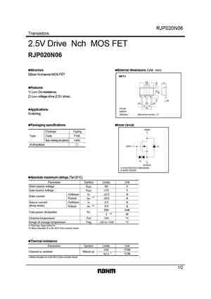
RJP020N06 Transistors 2.5V Drive Nch MOS FET RJP020N06 Structure External dimensions (Unit mm) Silicon N-channel MOS FET MPT3 4.5 1.5 1.6 Features 1) Low On-resistance. (1) (2) (3) 2) Low voltage drive (2.5V drive). 0.4 0.5 0.4 0.4 1.5 1.5 3.0 (1)Gate Applications (2)Drain Switching (3)Source Abbreviated symbol LS Packaging specifications Inner circu
rhp020n06t100.pdf

4V Drive Nch MOSFET RHP020N06 Structure Dimensions (Unit mm) Silicon N-channel MOSFET MPT3 4.5 1.5 1.6 Features 1) Low On-resistance. (1) (2) (3) 2) High speed switching. 0.4 3) Wide SOA. 0.5 0.4 0.4 1.5 1.5 3.0 (1)Gate (2)Drain (3)Source Abbreviated symbol LR Applications Switching Packaging specifications and hFE Inner circuit DRAIN Package Taping
rjp020n06t100.pdf

RJP020N06 Transistors 2.5V Drive Nch MOS FET RJP020N06 Structure External dimensions (Unit mm) Silicon N-channel MOS FET MPT3 4.5 1.5 1.6 Features 1) Low On-resistance. (1) (2) (3) 2) Low voltage drive (2.5V drive). 0.4 0.5 0.4 0.4 1.5 1.5 3.0 (1)Gate Applications (2)Drain Switching (3)Source Abbreviated symbol LS Packaging specifications Inner circu
rsr020n06.pdf
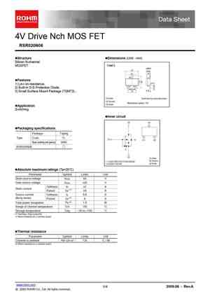
4V Drive Nch MOS FET RSR020N06 Structure Dimensions (Unit mm) Silicon N-channel MOSFET TSMT3 1.0MAX 2.9 0.85 0.4 0.7 (3) Features 1) Low on-resistance. (1) (2) 2) Built-in G-S Protection Diode. 0.95 0.95 0.16 3) Small Surface Mount Package (TSMT3) . 1.9 (1) Gate Each lead has same dimensions (2) Source Abbreviated symbol PZ (3) Drain Application Switching
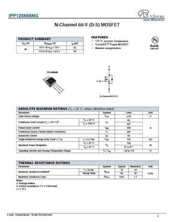
sqp120n06-06.pdf
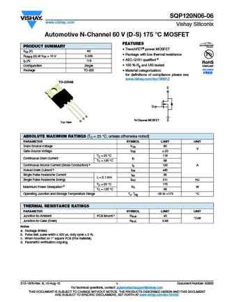
SQP120N06-06 www.vishay.com Vishay Siliconix Automotive N-Channel 60 V (D-S) 175 C MOSFET FEATURES PRODUCT SUMMARY TrenchFET power MOSFET VDS (V) 60 Package with low thermal resistance RDS(on) ( ) at VGS = 10 V 0.006 AEC-Q101 qualified d ID (A) 119 100 % Rg and UIS tested Configuration Single Package TO-220 Material categorization for definitions of co
sqm120n06-3m5l.pdf
SQM120N06-3m5L www.vishay.com Vishay Siliconix Automotive N-Channel 60 V (D-S) 175 C MOSFET FEATURES PRODUCT SUMMARY TrenchFET Power MOSFET VDS (V) 60 Package with Low Thermal Resistance RDS(on) ( ) at VGS = 10 V 0.0035 AEC-Q101 Qualifiedd RDS(on) ( ) at VGS = 4.5 V 0.0039 100 % Rg and UIS Tested ID (A) 120 Material categorization Configuration Single
sqm120n06-06.pdf
SQM120N06-06 www.vishay.com Vishay Siliconix Automotive N-Channel 60 V (D-S) 175 C MOSFET FEATURES PRODUCT SUMMARY TrenchFET power MOSFET VDS (V) 60 Package with low thermal resistance RDS(on) ( ) at VGS = 10 V 0.006 AEC-Q101 qualified d ID (A) 120 100 % Rg and UIS tested Configuration Single Package TO-263 Material categorization for definitions of co
sqm120n06-04l.pdf
SQM120N06-04L www.vishay.com Vishay Siliconix Automotive N-Channel 60 V (D-S) 175 C MOSFET FEATURES PRODUCT SUMMARY Halogen-free According to IEC 61249-2-21 VDS (V) 60 Definition RDS(on) ( ) at VGS = 10 V 0.0035 TrenchFET Power MOSFET RDS(on) ( ) at VGS = 4.5 V 0.0050 Package with Low Thermal Resistance ID (A) 120 AEC-Q101 Qualifiedd Configuration Single
ipg20n06s2l-35 ipg20n06s2l-35 ds 10.pdf

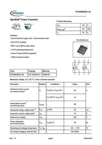
IPG20N06S2L-35 OptiMOS Power-Transistor Product Summary V 55 V DS 4) 35 m R DS(on),max I 20 A D Features Dual N-channel Logic Level - Enhancement mode PG-TDSON-8-4 AEC Q101 qualified MSL1 up to 260 C peak reflow 175 C operating temperature Green Product (RoHS compliant) 100% Avalanche tested Type Package Marking IPG20N06S2L-35 PG-TDSON-8-4 2N0
ipg20n06s2l-65a.pdf
IPG20N06S2L-65A OptiMOS Power-Transistor Product Summary VDS 55 V RDS(on),max3) 65 m ID 20 A Features Dual N-channel Logic Level - Enhancement mode PG-TDSON-8-10 AEC Q101 qualified MSL1 up to 260 C peak reflow 175 C operating temperature Green Product (RoHS compliant) 100% Avalanche tested Feasible for automatic optical inspection (AOI) Type
ipg20n06s4l-26a.pdf
IPG20N06S4L-26A OptiMOS -T2 Power-Transistor Product Summary VDS 60 V RDS(on),max4) 26 m ID 20 A Features Dual N-channel Logic Level - Enhancement mode PG-TDSON-8-10 AEC Q101 qualified MSL1 up to 260 C peak reflow 175 C operating temperature Green Product (RoHS compliant) 100% Avalanche tested Feasible for automatic optical inspection (AOI) Type
ipi020n06n.pdf
Type IPI020N06N OptiMOSTM Power-Transistor Features Product Summary Optimized for high performance SMPS, e.g. sync. rec. VDS 60 V 100% avalanche tested RDS(on),max 2.0 mW Superior thermal resistance ID 120 A N-channel QOSS nC 119 Qualified according to JEDEC1) for target applications QG(0V..10V) nC 106 Pb-free lead plating; RoHS compliant
ipg20n06s2l-50a.pdf
IPG20N06S2L-50A OptiMOS Power-Transistor Product Summary VDS 55 V RDS(on),max4) 50 m ID 20 A Features Dual N-channel Logic Level - Enhancement mode PG-TDSON-8-10 AEC Q101 qualified MSL1 up to 260 C peak reflow 175 C operating temperature Green Product (RoHS compliant) 100% Avalanche tested Feasible for automatic optical inspection (AOI) Type Pac
ipg20n06s4l-14 ipg20n06s4l-14 ds 1 0.pdf

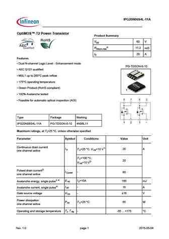
IPG20N06S4L-14 OptiMOS -T2 Power-Transistor Product Summary V 60 V DS 4) 13.7 mW R DS(on),max I 20 A D Features Dual N-channel Logic Level - Enhancement mode PG-TDSON-8-4 AEC Q101 qualified MSL1 up to 260 C peak reflow 175 C operating temperature Green Product (RoHS compliant) 100% Avalanche tested Type Package Marking IPG20N06S4L-14 PG-TDSON-8-4
ipd220n06l3 ipd220n06l3g.pdf
pe % # ! % (>.;?6?@ %>E Features D R #562= 7@C 9 89 7C6BF6?4J DH E49 ?8 2?5 DJ?4 C64 m D n) m x R ) AE > K65 E649?@=@8J 7@C 4@?G6CE6CD D R I46==6?E 82E6 492C86 I AC@5F4E ) ' D n) R ( 492??6= =@8 4 =6G6= R 2G2=2?496 E6DE65 R *3 7C66 A=2E ?8 , @"- 4@>A= 2?E 1) R + F2= 7 65 244@C5 ?8 E@ $ 7@C E2C86E 2AA= 42E @?D Type #* ( & ! Package G O Mark
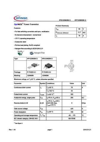
ipb120n06s4-03 ipi120n06s4-03 ipp120n06s4-03 ipp120n06s4 ipb120n06s4 ipi120n06s4-03.pdf

IPB120N06S4-03 IPI120N06S4-03, IPP120N06S4-03 OptiMOS -T2 Power-Transistor Product Summary V 60 V DS R (SMD version) 2.8 m DS(on),max I 120 A D Features N-channel - Enhancement mode PG-TO263-3-2 PG-TO262-3-1 PG-TO220-3-1 AEC Q101 qualified MSL1 up to 260 C peak reflow 175 C operating temperature Green Product (RoHS compliant) 100% Avalanche teste
ipg20n06s4l-26 ipg20n06s4l-26 ds 1 0.pdf

IPG20N06S4L-26 OptiMOS -T2 Power-Transistor Product Summary V 60 V DS 4) 26 mW R DS(on),max I 20 A D Features Dual N-channel Logic Level - Enhancement mode PG-TDSON-8-4 AEC Q101 qualified MSL1 up to 260 C peak reflow 175 C operating temperature Green Product (RoHS compliant) 100% Avalanche tested Type Package Marking IPG20N06S4L-26 PG-TDSON-8-4 4
ipg20n06s2l-65 ipg20n06s2l-65 ds 10.pdf
IPG20N06S2L-65 OptiMOS Power-Transistor Product Summary V 55 V DS 3) 65 m R DS(on),max I 20 A D Features Dual N-channel Logic Level - Enhancement mode PG-TDSON-8-4 AEC Q101 qualified MSL1 up to 260 C peak reflow 175 C operating temperature Green Product (RoHS compliant) 100% Avalanche tested Type Package Marking IPG20N06S2L-65 PG-TDSON-8-4 2N0
ipg20n06s2l-50 ipg20n06s2l-50 ds 10.pdf

IPG20N06S2L-50 OptiMOS Power-Transistor Product Summary V 55 V DS 4) 50 m R DS(on),max I 20 A D Features Dual N-channel Logic Level - Enhancement mode PG-TDSON-8-4 AEC Q101 qualified MSL1 up to 260 C peak reflow 175 C operating temperature Green Product (RoHS compliant) 100% Avalanche tested Type Package Marking IPG20N06S2L-50 PG-TDSON-8-4 2N0
ipp020n06n.pdf
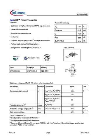
Type IPP020N06N OptiMOSTM Power-Transistor Features Product Summary Optimized for high performance SMPS, e.g. sync. rec. VDS 60 V 100% avalanche tested RDS(on),max 2.0 mW Superior thermal resistance ID 120 A N-channel QOSS nC 119 Qualified according to JEDEC1) for target applications QG(0V..10V) nC 106 Pb-free lead plating; RoHS compliant
ipg20n06s4l-11a.pdf
IPG20N06S4L-11A OptiMOS -T2 Power-Transistor Product Summary VDS 60 V RDS(on),max4) 11.2 mW ID 20 A Features Dual N-channel Logic Level - Enhancement mode PG-TDSON-8-10 AEC Q101 qualified MSL1 up to 260 C peak reflow 175 C operating temperature Green Product (RoHS compliant) 100% Avalanche tested Feasible for automatic optical inspection (AOI) Typ
ipg20n06s4l-11 ds 1 0.pdf

IPG20N06S4L-11 OptiMOS -T2 Power-Transistor Product Summary V 60 V DS 4) 11.2 mW R DS(on),max I 20 A D Features Dual N-channel Logic Level - Enhancement mode PG-TDSON-8-4 AEC Q101 qualified MSL1 up to 260 C peak reflow 175 C operating temperature Green Product (RoHS compliant) 100% Avalanche tested Type Package Marking IPG20N06S4L-11 PG-TDSON-8-4
ipg20n06s4-15 ipg20n06s4-15 ds 1 0.pdf
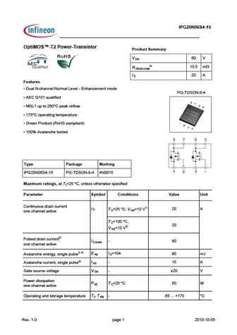
IPG20N06S4-15 OptiMOS -T2 Power-Transistor Product Summary V 60 V DS 4) 15.5 mW R DS(on),max I 20 A D Features Dual N-channel Normal Level - Enhancement mode PG-TDSON-8-4 AEC Q101 qualified MSL1 up to 260 C peak reflow 175 C operating temperature Green Product (RoHS compliant) 100% Avalanche tested Type Package Marking IPG20N06S4-15 PG-TDSON-8-4
ipb120n06ng ipp120n06ng.pdf
IPB120N06N G IPP120N06N G Power-Transistor Product Summary Features V D O >@ 50AB AE8B278=6 2>=D4@B4@A 0=3 AG=2 @42B85820B8>= R 11 7 m + >= = O ' 270==4; 4=70=24@?4@0B8=6 B4"+ 2>64= 5@44 022>@38=6 B> # Type #)) ' ' ! #) ' ' ! Package O 1 O
ipi120n06s4-h1 ipp120n06s4-h1 ipb120n06s4-h1.pdf
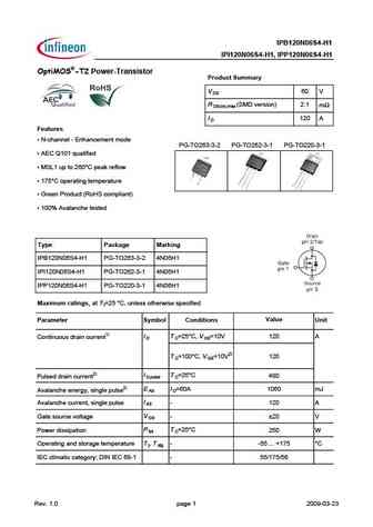
IPB120N06S4-H1 IPI120N06S4-H1, IPP120N06S4-H1 OptiMOS -T2 Power-Transistor Product Summary V 60 V DS R (SMD version) 2.1 m DS(on),max I 120 A D Features N-channel - Enhancement mode PG-TO263-3-2 PG-TO262-3-1 PG-TO220-3-1 AEC Q101 qualified MSL1 up to 260 C peak reflow 175 C operating temperature Green Product (RoHS compliant) 100% Avalanche teste
ipb120n06s4-h1 ipi120n06s4-h1 ipp120n06s4-h1.pdf

IPB120N06S4-H1 IPI120N06S4-H1, IPP120N06S4-H1 OptiMOS -T2 Power-Transistor Product Summary V 60 V DS R (SMD version) 2.1 m DS(on),max I 120 A D Features N-channel - Enhancement mode PG-TO263-3-2 PG-TO262-3-1 PG-TO220-3-1 AEC Q101 qualified MSL1 up to 260 C peak reflow 175 C operating temperature Green Product (RoHS compliant) 100% Avalanche teste
ipb120n06s4-02 ipi120n06s4-02 ipp120n06s4-02 ipp120n06s4 ipb120n06s4 ipi120n06s4-02.pdf
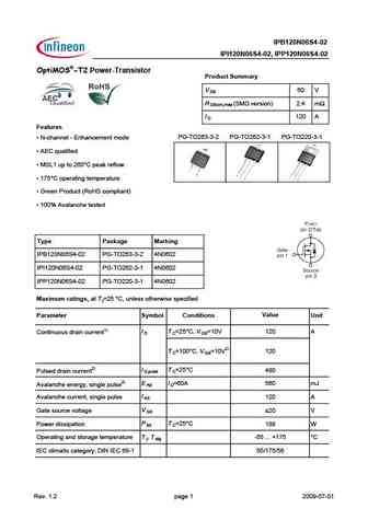
IPB120N06S4-02 IPI120N06S4-02, IPP120N06S4-02 OptiMOS -T2 Power-Transistor Product Summary V 60 V DS R (SMD version) 2.4 m DS(on),max I 120 A D Features PG-TO263-3-2 PG-TO262-3-1 PG-TO220-3-1 N-channel - Enhancement mode AEC qualified MSL1 up to 260 C peak reflow 175 C operating temperature Green Product (RoHS compliant) 100% Avalanche tested Ty

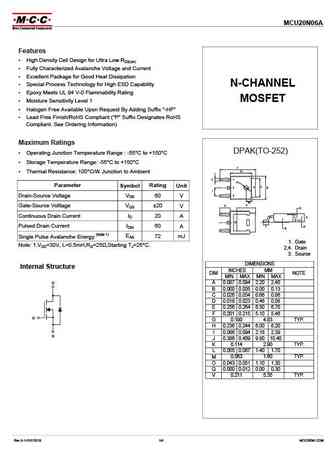
mcu20n06b.pdf

MCU20N06B Features High Density Cell Design for Ultra Low RDS(on) Fully Characterized Avalanche Voltage and Current Excellent Package for Good Heat Dissipation Special Process Technology for High ESD Capability N-CHANNEL Epoxy Meets UL 94 V-0 Flammability Rating MOSFET Moisture Sensitivity Level 1 Halogen Free Available Upon Request By Adding Suffix "-HF"
mcu20n06a.pdf
MCU20N06A Features High Density Cell Design for Ultra Low RDS(on) Fully Characterized Avalanche Voltage and Current Excellent Package for Good Heat Dissipation Special Process Technology for High ESD Capability N-CHANNEL Epoxy Meets UL 94 V-0 Flammability Rating MOSFET Moisture Sensitivity Level 1 Halogen Free Available Upon Request By Adding Suffix "-HF"
fqp20n06l.pdf

Is Now Part of To learn more about ON Semiconductor, please visit our website at www.onsemi.com Please note As part of the Fairchild Semiconductor integration, some of the Fairchild orderable part numbers will need to change in order to meet ON Semiconductor s system requirements. Since the ON Semiconductor product management systems do not have the ability to manage part nomenclatur
mtd20n06v-d.pdf
MTD20N06V Power Field Effect Transistor N-Channel DPAK TMOS V is a new technology designed to achieve an on-resistance http //onsemi.com area product about one-half that of standard MOSFETs. This new technology more than doubles the present cell density of our 50 and 60 V(BR)DSS RDS(on) TYP ID MAX volt TMOS devices. Just as with our TMOS E-FET designs, TMOS V is designed to withstand
fqp20n06.pdf

May 2001 TM QFET FQP20N06 60V N-Channel MOSFET General Description Features These N-Channel enhancement mode power field effect 20A, 60V, RDS(on) = 0.06 @VGS = 10 V transistors are produced using Fairchild s proprietary, Low gate charge ( typical 11.5 nC) planar stripe, DMOS technology. Low Crss ( typical 25 pF) This advanced technology has been especially tailored to
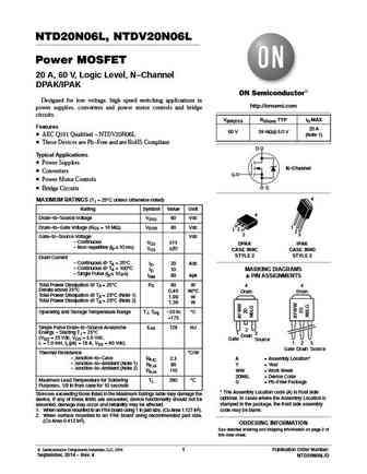
ntd20n06l ntdv20n06l.pdf
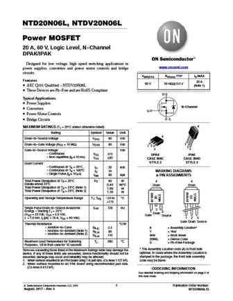
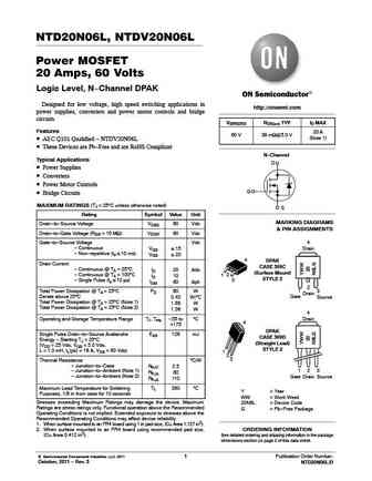
NTD20N06L, NTDV20N06L Power MOSFET 20 A, 60 V, Logic Level, N-Channel DPAK/IPAK Designed for low voltage, high speed switching applications in www.onsemi.com power supplies, converters and power motor controls and bridge circuits. V(BR)DSS RDS(on) TYP ID MAX Features 20 A 60 V 39 mW@5.0 V AEC Q101 Qualified - NTDV20N06L (Note 1) These Devices are Pb-Free and are RoHS Compli
ntd20n06lg.pdf
NTD20N06L, NTDV20N06L Power MOSFET 20 Amps, 60 Volts Logic Level, N-Channel DPAK Designed for low voltage, high speed switching applications in http //onsemi.com power supplies, converters and power motor controls and bridge circuits. V(BR)DSS RDS(on) TYP ID MAX Features 20 A 60 V 39 mW@5.0 V (Note 1) AEC Q101 Qualified - NTDV20N06L These Devices are Pb-Free and are RoHS C
fqd20n06.pdf
November 2013 FQD20N06 N-Channel QFET MOSFET 60 V, 16.8 A, 63 m Description Features This N-Channel enhancement mode power MOSFET is 16.8 A, 60 V, RDS(on) = 63 m (Max.) @ VGS = 10V, produced using Fairchild Semiconductor s proprietary ID = 8.4 A planar stripe and DMOS technology. This advanced Low Gate Charge (Typ.11.5 nC) MOSFET technology has been especially ta
nvmfd020n06c.pdf
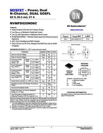
MOSFET - Power, Dual N-Channel, DUAL SO8FL 60 V, 20.3 mW, 27 A NVMFD020N06C Features www.onsemi.com Small Footprint (5x6 mm) for Compact Design Low RDS(on) to Minimize Conduction Losses Low QG and Capacitance to Minimize Driver Losses V(BR)DSS RDS(ON) MAX ID MAX NVMFWD020N06C - Wettable Flank Option for Enhanced Optical Inspection 60 V 20.3 mW @ 10 V 27 A AEC-Q1
ntmfs020n06c.pdf
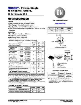
MOSFET- Power, Single N-Channel, SO8FL 60 V, 19.6 mW, 28 A NTMFS020N06C Features Small Footprint (5x6 mm) for Compact Design www.onsemi.com Low RDS(on) to Minimize Conduction Losses Low QG and Capacitance to Minimize Driver Losses These Devices are Pb-Free, Halogen Free/BFR Free and are RoHS V(BR)DSS RDS(ON) MAX ID MAX Compliant 60 V 19.6 mW @ 10 V 28 A Applications
ntmfd020n06c.pdf
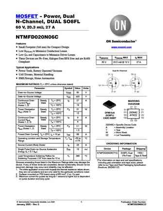
MOSFET - Power, Dual N-Channel, DUAL SO8FL 60 V, 20.3 mW, 27 A NTMFD020N06C Features www.onsemi.com Small Footprint (5x6 mm) for Compact Design Low RDS(on) to Minimize Conduction Losses Low QG and Capacitance to Minimize Driver Losses V(BR)DSS RDS(ON) MAX ID MAX These Devices are Pb-Free, Halogen Free/BFR Free and are RoHS Compliant 60 V 20.3 mW @ 10 V 27 A Typical
fqpf20n06.pdf

Is Now Part of To learn more about ON Semiconductor, please visit our website at www.onsemi.com Please note As part of the Fairchild Semiconductor integration, some of the Fairchild orderable part numbers will need to change in order to meet ON Semiconductor s system requirements. Since the ON Semiconductor product management systems do not have the ability to manage part nomenclatur
ntd20n06-001 ntd20n06-1g ntd20n06g.pdf
NTD20N06, NTDV20N06 Power MOSFET 20 Amps, 60 Volts, N-Channel DPAK Designed for low voltage, high speed switching applications in power supplies, converters and power motor controls and bridge circuits. Features Lower RDS(on) http //onsemi.com Lower VDS(on) Lower Capacitances V(BR)DSS RDS(on) TYP ID MAX Lower Total Gate Charge 60 V 37.5 mW 20 A Lower and Tighter
fqu20n06l.pdf

Is Now Part of To learn more about ON Semiconductor, please visit our website at www.onsemi.com Please note As part of the Fairchild Semiconductor integration, some of the Fairchild orderable part numbers will need to change in order to meet ON Semiconductor s system requirements. Since the ON Semiconductor product management systems do not have the ability to manage part nomenclatur
fdp020n06b.pdf

Is Now Part of To learn more about ON Semiconductor, please visit our website at www.onsemi.com Please note As part of the Fairchild Semiconductor integration, some of the Fairchild orderable part numbers will need to change in order to meet ON Semiconductor s system requirements. Since the ON Semiconductor product management systems do not have the ability to manage part nomenclatur
fdpf320n06l.pdf

Is Now Part of To learn more about ON Semiconductor, please visit our website at www.onsemi.com Please note As part of the Fairchild Semiconductor integration, some of the Fairchild orderable part numbers will need to change in order to meet ON Semiconductor s system requirements. Since the ON Semiconductor product management systems do not have the ability to manage part nomenclatur
nvmfs020n06c.pdf
MOSFET- Power, Single N-Channel, SO-8FL 60 V, 19.6 mW, 28 A NVMFS020N06C Features Small Footprint (5x6 mm) for Compact Design www.onsemi.com Low RDS(on) to Minimize Conduction Losses Low QG and Capacitance to Minimize Driver Losses NVMFWS020N06C - Wettable Flank Option for Enhanced Optical V(BR)DSS RDS(ON) MAX ID MAX Inspection 60 V 19.6 mW @ 10 V 28 A AEC-Q101
ntdv20n06.pdf
NTD20N06, NTDV20N06 Power MOSFET 20 A, 60 V, N-Channel DPAK Designed for low voltage, high speed switching applications in power supplies, converters and power motor controls and bridge circuits. Features http //onsemi.com Lower RDS(on) Lower VDS(on) V(BR)DSS RDS(on) TYP ID MAX Lower Capacitances 60 V 37.5 mW 20 A Lower Total Gate Charge Lower and Tighter VSD N
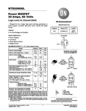
ntd20n06.pdf
NTD20N06 Power MOSFET 20 Amps, 60 Volts, N-Channel DPAK Designed for low voltage, high speed switching applications in power supplies, converters and power motor controls and bridge circuits. Features http //onsemi.com Lower RDS(on) Lower VDS(on) V(BR)DSS RDS(on) TYP ID MAX Lower Capacitances 60 V 37.5 mW 20 A Lower Total Gate Charge Lower and Tighter VSD N-Cha
ntdv20n06l.pdf
NTD20N06L, NTDV20N06L Power MOSFET 20 A, 60 V, Logic Level, N-Channel DPAK/IPAK Designed for low voltage, high speed switching applications in http //onsemi.com power supplies, converters and power motor controls and bridge circuits. V(BR)DSS RDS(on) TYP ID MAX Features 20 A 60 V 39 mW@5.0 V AEC Q101 Qualified - NTDV20N06L (Note 1) These Devices are Pb-Free and are RoHS Com
nttfs020n06c.pdf
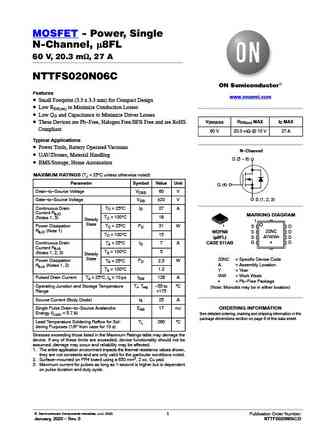
MOSFET - Power, Single N-Channel, m8FL 60 V, 20.3 mW, 27 A NTTFS020N06C Features www.onsemi.com Small Footprint (3.3 x 3.3 mm) for Compact Design Low RDS(on) to Minimize Conduction Losses Low QG and Capacitance to Minimize Driver Losses V(BR)DSS RDS(on) MAX ID MAX These Devices are Pb-Free, Halogen Free/BFR Free and are RoHS Compliant 60 V 20.3 mW @ 10 V 27 A Typica
nvtfs020n06c.pdf
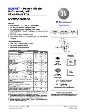
MOSFET - Power, Single N-Channel, m8FL 60 V, 20.3 mW, 27 A NVTFS020N06C Features www.onsemi.com Small Footprint (3.3 x 3.3 mm) for Compact Design Low RDS(on) to Minimize Conduction Losses Low QG and Capacitance to Minimize Driver Losses NVTFWS020N06C - Wettable Flank Option for Enhanced Optical V(BR)DSS RDS(on) MAX ID MAX Inspection 60 V 20.3 mW @ 10 V 27 A AEC-
utt120n06.pdf
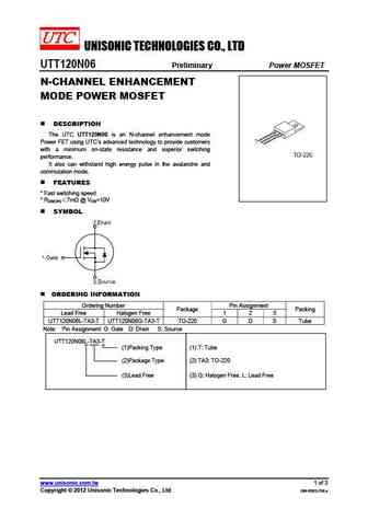
UNISONIC TECHNOLOGIES CO., LTD UTT120N06 Preliminary Power MOSFET N-CHANNEL ENHANCEMENT MODE POWER MOSFET DESCRIPTION The UTC UTT120N06 is an N-channel enhancement mode Power FET using UTC s advanced technology to provide customers with a minimum on-state resistance and superior switching performance. It also can withstand high energy pulse in the avalanche and commutati
utt20n06.pdf
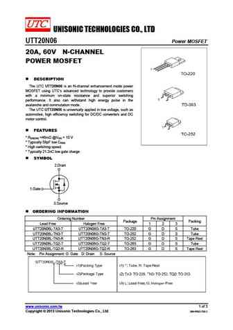
UNISONIC TECHNOLOGIES CO., LTD UTT20N06 Power MOSFET 20A, 60V N-CHANNEL POWER MOSFET DESCRIPTION The UTC UTT20N06 is an N-channel enhancement mode power MOSFET using UTC s advanced technology to provide customers with a minimum on-state resistance and superior switching performance. It also can withstand high energy pulse in the avalanche and commutation mode. The UTC U
sid20n06-90i.pdf
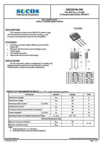
SID20N06-90I 19A, 60V, RDS(ON) 94 m N-Channel Enhancement MOSFET Elektronische Bauelemente RoHS Compliant Product A suffix of -C specifies halogen & lead-free TO-251P DESCRIPTION The miniature surface mount MOSFETs utilize a high cell density trench process to provide Low RDS(on) and to ensure minimal power loss and heat dissipation. FEATURES Low RDS(on) pro
ssd20n06-90d.pdf
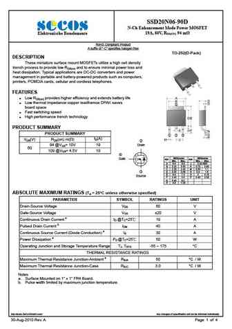
SSD20N06-90D N-Ch Enhancement Mode Power MOSFET 19A, 60V, RDS(ON) 94 m Elektronische Bauelemente RoHS Compliant Product A suffix of -C specifies halogen free TO-252(D-Pack) DESCRIPTION These miniature surface mount MOSFETs utilize a high cell density trench process to provide low RDS(on) and to ensure minimal power loss and heat dissipation. Typical applications are
cju20n06.pdf
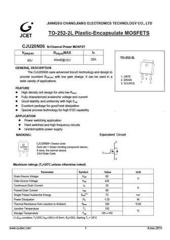
JIANGSU CHANGJIANG ELECTRONICS TECHNOLOGY CO., LTD TO-252-2L Plastic-Encapsulate MOSFETS CJU20N06 N-Channel Power MOSFET ID V(BR)DSS RDS(on)MAX TO-252-2L 20A 45m @10V 60V GENERAL DESCRIPTION The CJU20N06 uses advanced trench technology and design to 1. GATE provide excellent RDS(ON) with low gate charge. It can be used in a 2. DRAIN wide variety of applications.
am20n06-90i.pdf
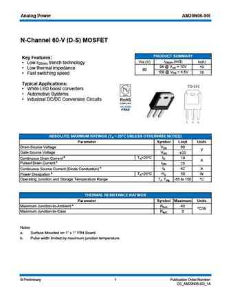
Analog Power AM20N06-90I N-Channel 60-V (D-S) MOSFET PRODUCT SUMMARY Key Features rDS(on) (m ) VDS (V) ID(A) Low r trench technology DS(on) 94 @ VGS = 10V 19 Low thermal impedance 60 109 @ VGS = 4.5V 18 Fast switching speed Typical Applications White LED boost converters Automotive Systems Industrial DC/DC Conversion Circuits ABSOLUTE MAXIMU
am20n06-90d.pdf
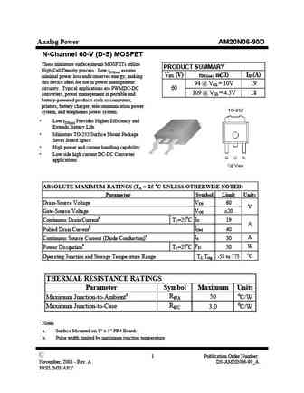
Analog Power AM20N06-90D N-Channel 60-V (D-S) MOSFET These miniature surface mount MOSFETs utilize PRODUCT SUMMARY High Cell Density process. Low rDS(on) assures VDS (V) rDS(on) m( ) ID (A) minimal power loss and conserves energy, making this device ideal for use in power management 94 @ VGS = 10V 19 circuitry. Typical applications are PWMDC-DC 60 109 @ VGS = 4.5V 18 converters
jt020n065sed jt020n065ced jt020n065wed jt020n065fed.pdf

N N-CHANNEL IGBT R JT020N065SED/CED/WED/FED MAIN CHARACTERISTICS Package I 20 A C BV 650V CES V CESAT-typ 1.6V V =15V GE APPLICATIONS General purpose inverters UPS UPS TO-263 FEATURES TO-220C Low gate charge Trenc
mtb20n06kj3.pdf
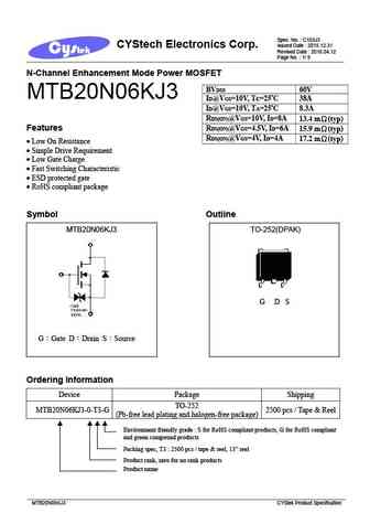
Spec. No. C103J3 Issued Date 2015.12.31 CYStech Electronics Corp. Revised Date 2018.04.12 Page No. 1/ 9 N-Channel Enhancement Mode Power MOSFET BVDSS 60V MTB20N06KJ3 ID@VGS=10V, TC=25 C 38A ID@VGS=10V, TA=25 C 8.3A RDS(ON)@VGS=10V, ID=8A 13.4 m (typ) Features RDS(ON)@VGS=4.5V, ID=6A 15.9 m (typ) RDS(ON)@VGS=4V, ID=4A 17.2 m (typ) Low On Resistance
mtb20n06j3.pdf
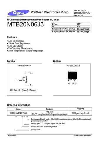
Spec. No. C925J3 Issued Date 2013.08.13 CYStech Electronics Corp. Revised Date 2013.12.30 Page No. 1/ 9 N-Channel Enhancement Mode Power MOSFET BVDSS 60V MTB20N06J3 ID 42A RDS(ON)@VGS=10V, ID=20A 14.6 m (typ) RDS(ON)@VGS=4.5V, ID=20A 16.7 m (typ) Features Low On Resistance Simple Drive Requirement Low Gate Charge Fast Switching Characteristic
g20n06j.pdf
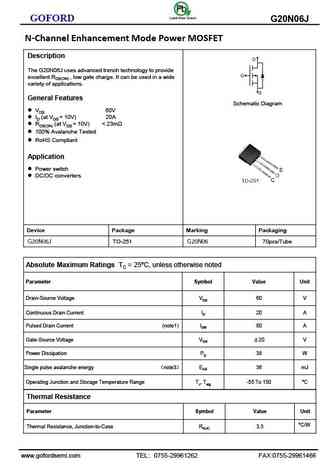
GOFORD G20N06J N-Channel Enhancement Mode Power MOSFET Description The G20N06J uses advanced trench technology to provide excellent RDS(ON) , low gate charge. It can be used in a wide variety of applications. General Features Schematic Diagram VDS 60V ID (at VGS = 10V) 20A RDS(ON) (at VGS = 10V)
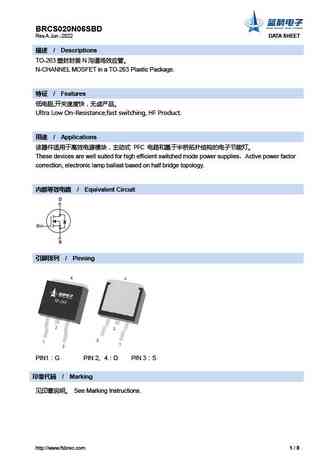
brcs020n06sra.pdf
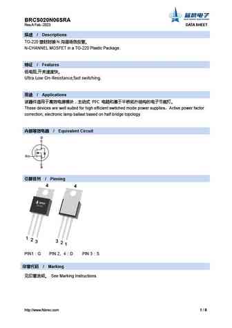
BRCS020N06SRA Rev.A Feb.-2023 DATA SHEET / Descriptions TO-220 N N-CHANNEL MOSFET in a TO-220 Plastic Package. / Features , Ultra Low On-Resistance,fast switching. / Applications PFC These d
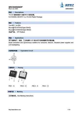
brcs20n06ip.pdf
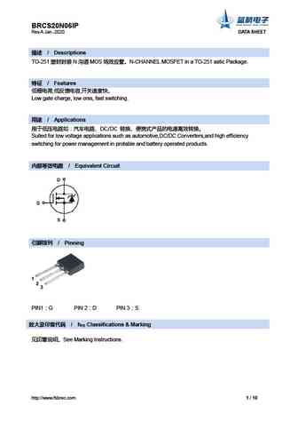
BRCS20N06IP Rev.A Jan.-2020 DATA SHEET / Descriptions TO-251 N MOS N-CHANNEL MOSFET in a TO-251 astic Package. / Features , , Low gate charge, low crss, fast switching. / Applications DC/DC S
brcs120n06ha.pdf
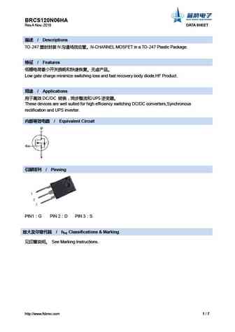
BRCS120N06HA Rev.A Nov.-2018 DATA SHEET / Descriptions TO-247 N N-CHANNEL MOSFET in a TO-247 Plastic Package. / Features Low gate charge minimize switching loss and fast recovery body diode.HF Product. / Applications DC/DC
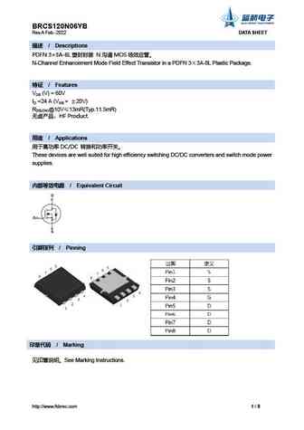
brcs120n06sym.pdf
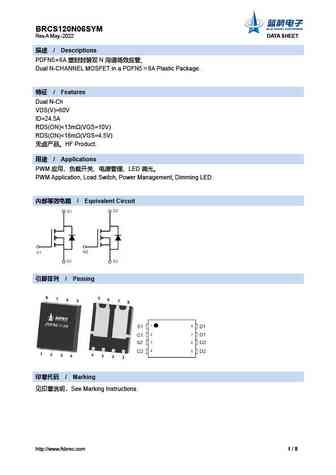
BRCS120N06SYM Rev.A May.-2022 DATA SHEET / Descriptions PDFN5 6A N Dual N-CHANNEL MOSFET in a PDFN5 6A Plastic Package. / Features Dual N-Ch VDS(V)=60V ID=24.5A RDS(ON)
crte120n06l.pdf
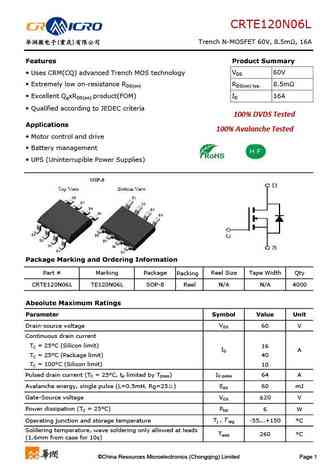
CRTE120N06L ( ) Trench N-MOSFET 60V, 8.5m , 16A Features Product Summary VDS Uses CRM(CQ) advanced Trench MOS technology 60V Extremely low on-resistance RDS(on) RDS(on) typ. 8.5m Excellent QgxRDS(on) product(FOM) ID 16A Qualified according to JEDEC criteria 100% DVDS Tested 100% DVDS Tested 100% DVDS Tested Applications 100% Aval
cm120n06.pdf
R CM120N06 www.jdsemi.cn ShenZhen Jingdao Electronic Co.,Ltd. POWER MOSFET 60V N-Channel Trench-MOS RoHS 1 US P 2 3
kx020n06.pdf
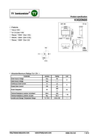
MOSFET e IC SMD Type SMDType IC DIP Type IC SMDType MOSFET DIP Type MOSFET SMD Type SMD Type Product specification KX020N06 Features VDS (V) = 60V ID = 2 A (VGS = 10V) 200m (V = 10V) DS(ON) GS R 280m (V = 4.5V) DS(ON) GS R RDS
ftk20n06d.pdf
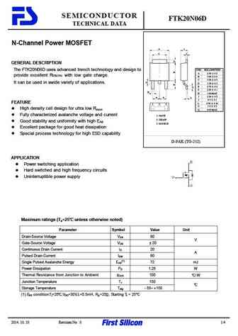
SEMICONDUCTOR FTK20N06D TECHNICAL DATA N-Channel Power MOSFET A I C J GENERAL DESCRIPTION The FTK20N06D uses advanced trench technology and design to DIM MILLIMETERS A 6 50 0 2 provide excellent RDS(ON) with low gate charge. B 5 60 0 2 C 5 20 0 2 It can be used in awide variety of applications. D 1 50 0 2 E 2 70 0 2 F 2 30 0 1 H H 1 00 MAX I 2 30 0
kx120n06.pdf
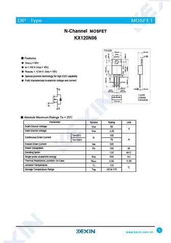
DIP Type MOSFET N-Channel MOSFET KX120N06 TO-220 9.90 0.20 4.50 0.20 (8.70) +0.10 3.60 0.10 1.30 0.05 Features VDS (V) = 60V ID = 100 A (VGS = 10V) RDS(ON) 6.5m (VGS = 10V) Special process technology for high ESD capability Fully characterized Avalanche voltage and current 1.27 0.10 1.52 0.10 2 1 3 0.80 0.10 +0.10 0.50
rhp020n06.pdf
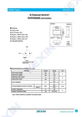
SMD Type MOSFET N-Channel MOSFET RHP020N06 (KHP020N06) SOT-89 Unit mm 1.70 0.1 Features VDS (V) = 60V ID = 2 A (VGS = 10V) RDS(ON) 200m (VGS = 10V) RDS(ON) 280m (VGS = 4.5V) 0.42 0.1 0.46 0.1 RDS(ON) 340m (VGS = 4V) High speed switching 1.Gate 2.Drain 3.Source DRAIN GATE *2 *1 SOURCE *1 ESD PROTECTION DIODE *2 BODY DIOD
ms20n06.pdf
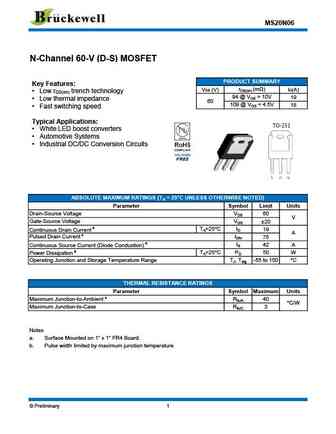
MS20N06 N-Channel 60-V (D-S) MOSFET PRODUCT SUMMARY Key Features rDS(on) (m ) VDS (V) ID(A) Low r trench technology DS(on) 94 @ VGS = 10V 19 Low thermal impedance 60 109 @ VGS = 4.5V 18 Fast switching speed Typical Applications White LED boost converters Automotive Systems Industrial DC/DC Conversion Circuits ABSOLUTE MAXIMUM RATINGS (TA = 25 C U
mse20n06n.pdf
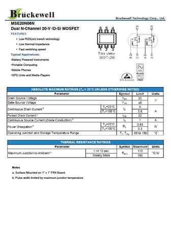
Bruckewell Technology Corp., Ltd. MSE20N06N Dual N-Channel 20-V (D-S) MOSFET FEATURES Low RDS(on) trench technology Low thermal impedance Fast switching speed Typical Applications Battery Powered Instruments Portable Computing Mobile Phones GPS Units and Media Players Notes a. Surface Mounted on 1 x 1 FR4 Board. b. Pulse width limited
msd20n06.pdf

MSD20N06 N-Channel 60-V (D-S) MOSFET Description The MSD20N06 is a N-channel enhancement-mode MOSFET , providing the designer with the best combination of fast switching, ruggedized device design, low on-resistance and cost effectiveness. The TO-252 package is universally preferred for all commercial-industrial applications Features White LED boost converters Autom
wfd20n06.pdf
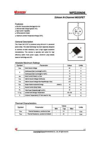
WFD20N06 Silicon N-Channel MOSFET Features 20A,60V, RDS(on)(Max 39m )@VGS=10V Ultra-low Gate Charge(Typical 6.1nC) High Current Capability 100%Avalanche Tested Maximum Junction Temperature Range(150 ) General Description This Power MO S FET is produced using Win se m i s advanced planar stripe, This latest technology has been especially designed t
wfu20n06.pdf
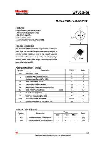
WFU20N06 Silicon N-Channel MOSFET Features 20A,60V, RDS(on)(Max 39m )@VGS=10V Ultra-low Gate Charge(Typical 6.1nC) High Current Capability 100%Avalanche Tested Maximum Junction Temperature Range(150 ) General Description This Power MO S FET is produced using Win se m i s advanced planar stripe, This latest technology has been especially designed to
chm20n06pagp.pdf
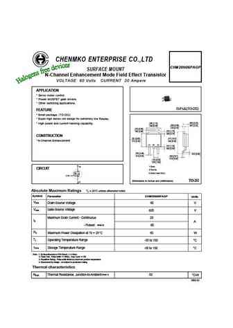
CHENMKO ENTERPRISE CO.,LTD CHM20N06PAGP SURFACE MOUNT N-Channel Enhancement Mode Field Effect Transistor VOLTAGE 60 Volts CURRENT 20 Ampere APPLICATION * Servo motor control. * Power MOSFET gate drivers. * Other switching applications. D-PAK(TO-252) FEATURE * Small package. (TO-252) * Super high dense cell design for extremely low RDS(ON). .094 (2.40) .280 (7.10) * High power
slm120n06g.pdf
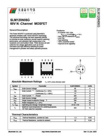
SLM120N06G 60V N -Channel MOSFET General Description Features - N-Channel 60V 120A This Power MOSFET is produced using Msemitek s RDS(on)Typ=2.6m @VGS = 10 V advanced Shielded Gate Trench MOSFET technology. - Very Low On-resistance RDS(ON) This advanced technology has been especially tailored - Low Crss to minimize on-state resistance, provide superior switching - Fast swit
wmq20n06ts.pdf
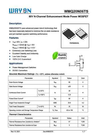
WMQ20N06TS 60V N-Channel Enhancement Mode Power MOSFET Description WMQ20N06TS uses advanced power trench technology that D D D D D D has been especially tailored to minimize the on-state resistance D D and yet maintain superior switching performance. S G S S S Features S G S V = 60V, I = 20A DS D PDFN3030-8L R
wmm020n06hg4.pdf
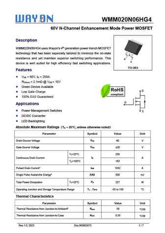
WMM020N06HG4 60V N-Channel Enhancement Mode Power MOSFET Description WMM020N06HG4 uses Wayon's 4th generation power trench MOSFET technology that has been especially tailored to minimize the on-state D resistance and yet maintain superior switching performance. This G S device is well suited for high efficiency fast switching applications. TO-263 Features V = 60V, I = 25
wmk020n06hg4.pdf
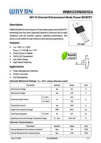
WMK020N06HG4 60V N-Channel Enhancement Mode Power MOSFET Description WMK020N06HG4 uses Wayon's 4th generation power trench MOSFET technology that has been especially tailored to minimize the on-state resistance and yet maintain superior switching performance. This device is well suited for high efficiency fast switching applications. S D G Features TO-220 V = 60V, I = 25
wmb020n06hg4.pdf
WMB020N06HG4 60V N-Channel Enhancement Mode Power MOSFET Description D D D D WMB020N06HG4 uses Wayon's 4th generation power trench MOSFET D D D D technology that has been especially tailored to minimize the on-state G ss resistance and yet maintain superior switching performance. This device s ss G s is well suited for high efficiency fast switching applications. PDFN5
fir20n06lg.pdf
FIR20N06LG N-Channel Enhancement Mode Power Mosfet PIN Connection TO-252 Description TheFIR20N06LG uses advanced trench technology and design to provide excellent RDS(ON) with low gate charge. It can be used in a wide variety of applications. General Features VDS =60V,ID =20A RDS(ON)
dac020n065z1.pdf

DAC020N065Z1 DACO SEMICONDUCTOR CO., LTD. Silicon Carbide Enhancement Mode MOSFET VDSS 650V Features I 107A D(@25 ) Drain RDS(ON) 20m (Pin1, TAB) TO-247-4L Package Gate
ptd20n06.pdf
PTD20N06 60 N-Channel Advanced Power MOSFET 0V/20A Features General Features Low On-Resistance VDS =60V,ID =20A Fast Switching RDS(ON)
hgs120n06sl.pdf
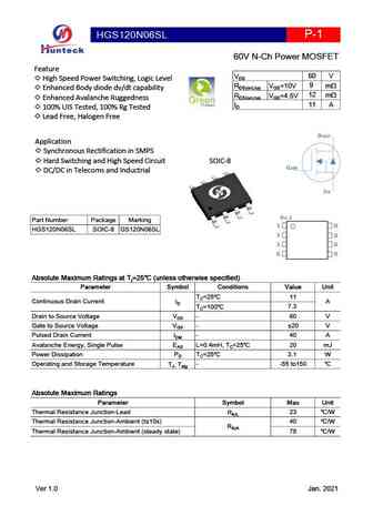
HGS120N06SL P-1 60V N-Ch Power MOSFET Feature 60 V VDS High Speed Power Switching, Logic Level 9 RDS(on),typ VGS=10V mW Enhanced Body diode dv/dt capability 12 RDS(on),typ VGS=4.5V mW Enhanced Avalanche Ruggedness 11 A ID 100% UIS Tested, 100% Rg Tested Lead Free, Halogen Free Drain Application Synchronous Rectification in SMPS Hard Switching and H
hgd120n06sl hgi120n06sl.pdf
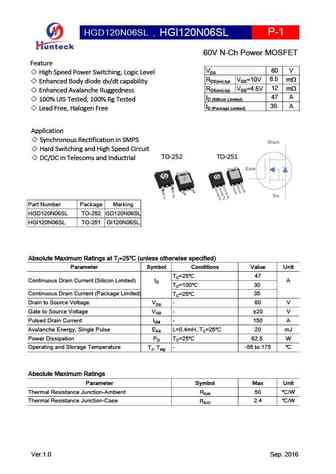
HGD120N06SL , HGI120N06SL P-1 60V N-Ch Power MOSFET Feature 60 V VDS High Speed Power Switching, Logic Level 8.5 RDS(on),typ VGS=10V m Enhanced Body diode dv/dt capability 12 RDS(on),typ VGS=4.5V m Enhanced Avalanche Ruggedness 47 A ID (Sillicon Limited) 100% UIS Tested, 100% Rg Tested 35 A ID (Package Limited) Lead Free, Halogen Free Application
hgm120n06sl.pdf
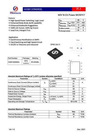
HGM120N06SL P-1 60V N-Ch Power MOSFET Feature 60 V VDS High Speed Power Switching, Logic Level 8.5 RDS(on),typ VGS=10V mW Enhanced Body diode dv/dt capability 12 RDS(on),typ VGS=4.5V mW Enhanced Avalanche Ruggedness 33 A ID (Sillicon Limited) 100% UIS Tested, 100% Rg Tested 26 A Lead Free, Halogen Free ID (Package Limited) Application Synchronous
hgn120n06sl.pdf
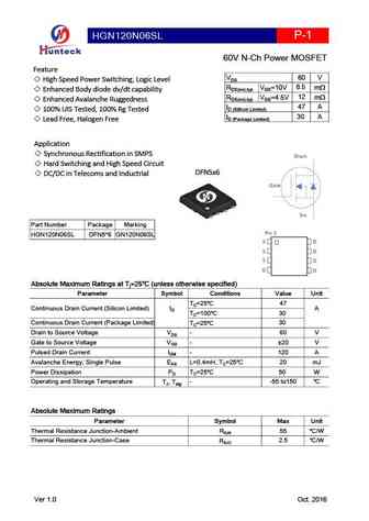
HGN120N06SL P-1 60V N-Ch Power MOSFET Feature 60 V VDS High Speed Power Switching, Logic Level 8.5 RDS(on),typ VGS=10V m Enhanced Body diode dv/dt capability 12 RDS(on),typ VGS=4.5V m Enhanced Avalanche Ruggedness 47 A ID (Sillicon Limited) 100% UIS Tested, 100% Rg Tested 30 A ID (Package Limited) Lead Free, Halogen Free Application Synchronous R
wsf20n06.pdf
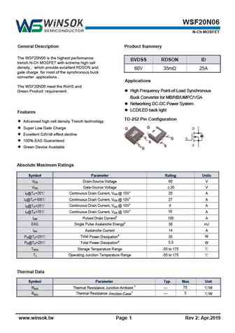
WSF20N06 N-Ch MOSFET General Description Product Summery The WSF20N06 is the highest performance BVDSS RDSON ID trench N-Ch MOSFET with extreme high cell density , which provide excellent RDSON and 60V 35m 25A gate charge for most of the synchronous buck converter applications . Applications The WSF20N06 meet the RoHS and High Frequency Point-of-Load Synchronous Gree
fqp20n06l.pdf
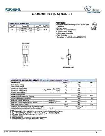
FQP20N06L www.VBsemi.tw N-Channel 60 V (D-S) MOSFET FEATURES PRODUCT SUMMARY Halogen-free According to IEC 61249-2-21 VDS (V) RDS(on) ( ) ID (A)a, e Qg (Max) Definition Surface Mount 0.024 at VGS = 10 V 50 60 66 nC Available in Tape and Reel 0.028 at VGS = 4.5 V 40 Dynamic dV/dt Rating Logic-Level Gate Drive Fast Switching Compliant to RoHS Di
mtd20n06hdlt4g.pdf
MTD20N06HDLT4G www.VBsemi.tw N-Channel 6 0-V (D-S) MOSFET FEATURES PRODUCT SUMMARY TrenchFET Power MOSFET VDS (V) rDS(on) ( ) ID (A)a Available 175 C Junction Temperature 0.025 at VGS = 10 V 35 RoHS* 60 0.030 at VGS = 4.5 V 30 COMPLIANT TO-252 D G Drain Connected to Tab G D S S Top View N-Channel MOSFET ABSOLUTE MAXIMUM RATINGS TC = 25 C, unless otherwis
cmd20n06l.pdf

CMD20N06L www.VBsemi.tw N-Channel 6 0-V (D-S) MOSFET FEATURES PRODUCT SUMMARY TrenchFET Power MOSFET VDS (V) rDS(on) ( ) ID (A)a Available 175 C Junction Temperature 0.025 at VGS = 10 V 35 RoHS* 60 0.030 at VGS = 4.5 V 30 COMPLIANT TO-252 D G Drain Connected to Tab G D S S Top View N-Channel MOSFET ABSOLUTE MAXIMUM RATINGS TC = 25 C, unless otherwise n
fqd20n06.pdf

FQD20N06 www.VBsemi.tw N-Channel 6 0-V (D-S) MOSFET FEATURES PRODUCT SUMMARY TrenchFET Power MOSFET VDS (V) rDS(on) ( ) ID (A)a Available 175 C Junction Temperature 0.025 at VGS = 10 V 35 RoHS* 60 0.030 at VGS = 4.5 V 30 COMPLIANT TO-252 D G Drain Connected to Tab G D S S Top View N-Channel MOSFET ABSOLUTE MAXIMUM RATINGS TC = 25 C, unless otherwise note
rsr020n06tl.pdf
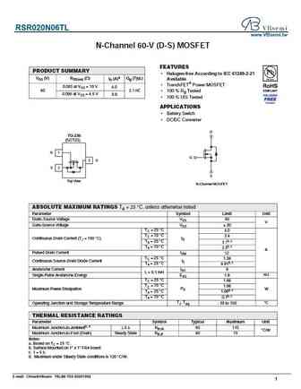
RSR020N06TL www.VBsemi.tw N-Channel 60-V (D-S) MOSFET FEATURES PRODUCT SUMMARY Halogen-free According to IEC 61249-2-21 VDS (V) RDS(on) ( ) ID (A)a Qg (Typ.) Available TrenchFET Power MOSFET 0.085 at VGS = 10 V 4.0 60 2.1 nC 100 % Rg Tested 0.096 at VGS = 4.5 V 3.8 100 % UIS Tested APPLICATIONS Battery Switch DC/DC Converter D TO-236 (SOT23)
ntd20n06lt4g.pdf
NTD20N06LT4G www.VBsemi.tw N-Channel 6 0-V (D-S) MOSFET FEATURES PRODUCT SUMMARY TrenchFET Power MOSFET VDS (V) rDS(on) ( ) ID (A)a Available 175 C Junction Temperature 0.025 at VGS = 10 V 35 RoHS* 60 0.030 at VGS = 4.5 V 30 COMPLIANT TO-252 D G Drain Connected to Tab G D S S Top View N-Channel MOSFET ABSOLUTE MAXIMUM RATINGS TC = 25 C, unless otherwise
ceu20n06.pdf
CEU20N06 www.VBsemi.tw N-Channel 6 0-V (D-S) MOSFET FEATURES PRODUCT SUMMARY TrenchFET Power MOSFET VDS (V) rDS(on) ( ) ID (A)a Available 175 C Junction Temperature 0.025 at VGS = 10 V 35 RoHS* 60 0.030 at VGS = 4.5 V 30 COMPLIANT TO-252 D G Drain Connected to Tab G D S S Top View N-Channel MOSFET ABSOLUTE MAXIMUM RATINGS TC = 25 C, unless otherwise no
fqd20n06le.pdf

FQD20N06LE www.VBsemi.tw N-Channel 6 0-V (D-S) MOSFET FEATURES PRODUCT SUMMARY TrenchFET Power MOSFET VDS (V) rDS(on) ( ) ID (A)a Available 175 C Junction Temperature 0.025 at VGS = 10 V 35 RoHS* 60 0.030 at VGS = 4.5 V 30 COMPLIANT TO-252 D G Drain Connected to Tab G D S S Top View N-Channel MOSFET ABSOLUTE MAXIMUM RATINGS TC = 25 C, unless otherwise
rjp020n06t100.pdf
RJP020N06T100 www.VBsemi.tw N-Channel 60-V (D-S) MOSFET FEATURES PRODUCT SUMMARY Halogen-free VDS (V) RDS(on) ( ) ID (A)a Qg (Typ.) TrenchFET Power MOSFET 0.076 at VGS = 4.5 V 7.1 RoHS 29 nC COMPLIANT 60 APPLICATIONS 0.088 at VGS = 10 V 6.7 Load Switches for Portable Devices D D G S G D S N-Channel MOSFET ABSOLUTE MAXIMUM RATINGS TA = 25 C, unless otherw
ipb120n06ng.pdf
IPB120N06NG www.VBsemi.tw N-Channel 60-V (D-S) MOSFET FEATURES PRODUCT SUMMARY 175 C Junction Temperature VDS (V) RDS(on) ( ) ID (A)a TrenchFET Power MOSFET 0.012 at VGS = 10 V 60 60 0.013 at VGS = 4.5 V 50 D D2PAK (TO-263) G G D S S N-Channel MOSFET ABSOLUTE MAXIMUM RATINGS (TC = 25 C, unless otherwise noted) Parameter Symbol Limit Unit VGS Gate-Sou
ipp120n06ng.pdf
IPP120N06NG www.VBsemi.tw N-Channel 60-V (D-S) MOSFET FEATURES PRODUCT SUMMARY 175 C Junction Temperature VDS (V) RDS(on) ( ) ID (A)a TrenchFET Power MOSFET 0.011 at VGS = 10 V 60 Material categorization 60 0.012 at VGS = 4.5 V 50 D TO-220AB G S D S G N-Channel MOSFET ABSOLUTE MAXIMUM RATINGS (TC = 25 C, unless otherwise noted) Parameter Symbol Li
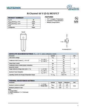
vbzfb20n06.pdf
VBZFB20N06 www.VBsemi.com N-Channel 60 V (D-S) MOSFET FEATURES PRODUCT SUMMARY 175 C Junction Temperature VDS (V) 60 TrenchFET Power MOSFET RDS(on) ( ) at VGS = 10 V 0.020 Material categorization RDS(on) ( ) at VGS = 4.5 V 0.025 ID (A) 35 Configuration Single TO-251 D G S N-Channel MOSFET G D S Top View ABSOLUTE MAXIMUM RATINGS (TC = 25 C, unless other
20n06l-to252.pdf

20N06L TO252 www.VBsemi.tw N-Channel 6 0-V (D-S) MOSFET FEATURES PRODUCT SUMMARY TrenchFET Power MOSFET VDS (V) rDS(on) ( ) ID (A)a Available 175 C Junction Temperature 0.025 at VGS = 10 V 35 RoHS* 60 0.030 at VGS = 4.5 V 30 COMPLIANT TO-252 D G Drain Connected to Tab G D S S Top View N-Channel MOSFET ABSOLUTE MAXIMUM RATINGS TC = 25 C, unless otherwise
vbze20n06.pdf
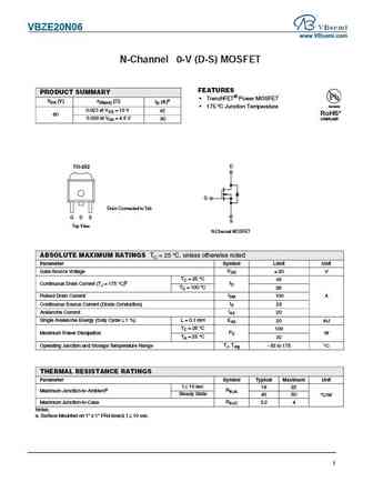
VBZE20N06 www.VBsemi.com N-Channel 6 0-V (D-S) MOSFET FEATURES PRODUCT SUMMARY TrenchFET Power MOSFET VDS (V) rDS(on) ( ) ID (A)a Available 175 C Junction Temperature 0.023 at VGS = 10 V 45 RoHS* 60 0.030 at VGS = 4.5 V 30 COMPLIANT TO-252 D G Drain Connected to Tab G D S S Top View N-Channel MOSFET ABSOLUTE MAXIMUM RATINGS TC = 25 C, unless otherwise no
ntd20n06t4.pdf
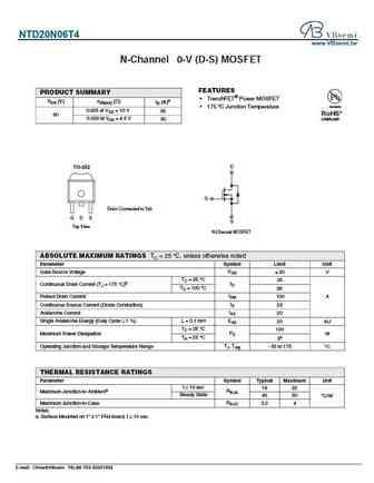
NTD20N06T4 www.VBsemi.tw N-Channel 6 0-V (D-S) MOSFET FEATURES PRODUCT SUMMARY TrenchFET Power MOSFET VDS (V) rDS(on) ( ) ID (A)a Available 175 C Junction Temperature 0.025 at VGS = 10 V 35 RoHS* 60 0.030 at VGS = 4.5 V 30 COMPLIANT TO-252 D G Drain Connected to Tab G D S S Top View N-Channel MOSFET ABSOLUTE MAXIMUM RATINGS TC = 25 C, unless otherwise no
yjd20n06a.pdf
RoHS COMPLIANT YJD20N06A N-Channel Enhancement Mode Field Effect Transistor Product Summary V 60V DS I 20A D R ( at V =10V) 43mohm DS(ON) GS R ( at V =4.5V) 47 mohm DS(ON) GS 100% UIS Tested 100% VDS Tested General Description Trench Power MV MOSFET technology Excellent package for heat dissipation High density cell d
hm20n06.pdf
N-Channel Enhancement Mode Power MOSFET Description The uses advanced trench technology and design to provide excellent RDS(ON) with low gate charge. It can be used in a wide variety of applications. General Features VDS =60V,ID =20A RDS(ON)
hm20n06ka.pdf
HM20N06KA N-Channel Enhancement Mode Power MOSFET Description The HM20N06KA uses advanced trench technology and design to provide excellent RDS(ON) with low gate charge. It can be used in a wide variety of applications. General Features VDS =60V,ID =20A RDS(ON)
hm20n06ia.pdf
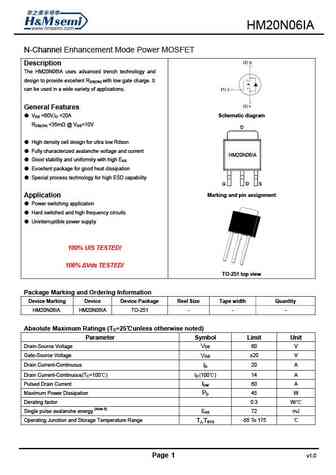
N-Channel Enhancement Mode Power MOSFET Description The uses advanced trench technology and design to provide excellent RDS(ON) with low gate charge. It can be used in a wide variety of applications. General Features VDS =60V,ID =20A Schematic diagram RDS(ON)
mpg120n06p mpg120n06s.pdf
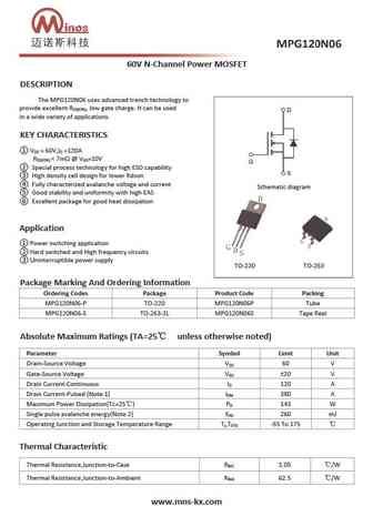
60V N-Channel Power MOSFET DESCRIPTION The MPG120N06 uses advanced trench technology to provide excellent R , low gate charge. It can be used DS(ON) in a wide variety of applications. KEY CHARACTERISTICS V = 60V,I =120A DS D R
mdt20n06.pdf
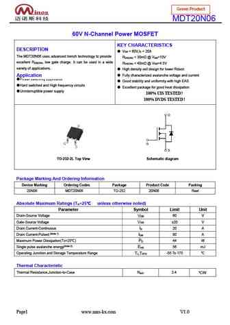
Green Product MDT20N06 60V N-Channel Power MOSFET KEY CHARACTERISTICS DESCRIPTION V = 60V,I = 20A DS D The MDT20N06 uses advanced trench technology to provide R
fqp20n06l.pdf
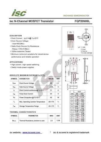
INCHANGE Semiconductor isc N-Channel MOSFET Transistor FQP20N06L DESCRIPTION Drain Current I =21A@ T =25 D C Drain Source Voltage- V =60V(Min) DSS Static Drain-Source On-Resistance R = 55m (Max) DS(on) 100% Avalanche Tested Minimum Lot-to-Lot variations for robust device performance and reliable operation APPLICATIONS High current , high speed switching Swi
ipp020n06n.pdf
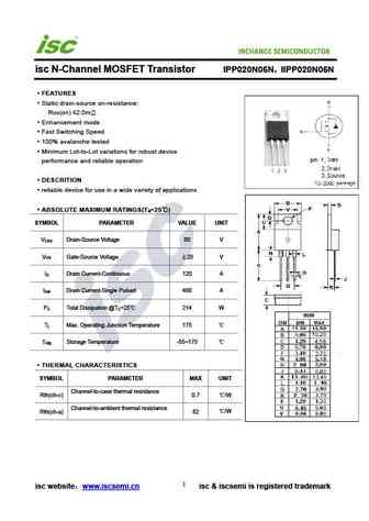
INCHANGE Semiconductor isc N-Channel MOSFET Transistor IPP020N06N IIPP020N06N FEATURES Static drain-source on-resistance RDS(on) 2.0m Enhancement mode Fast Switching Speed 100% avalanche tested Minimum Lot-to-Lot variations for robust device performance and reliable operation DESCRITION reliable device for use in a wide variety of applications ABSOLUTE MAX
ipd220n06l3.pdf
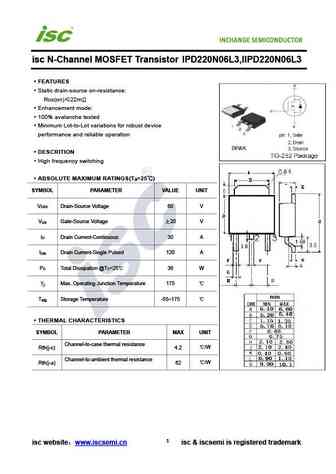
isc N-Channel MOSFET Transistor IPD220N06L3,IIPD220N06L3 FEATURES Static drain-source on-resistance RDS(on) 22m Enhancement mode 100% avalanche tested Minimum Lot-to-Lot variations for robust device performance and reliable operation DESCRITION High frequency switching ABSOLUTE MAXIMUM RATINGS(T =25 ) a SYMBOL PARAMETER VALUE UNIT V Drain-Source Voltage 60
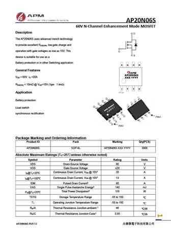
ap20n06s.pdf
AP20N06S 60V N-Channel Enhancement Mode MOSFET Description The AP20N06S uses advanced trench technology to provide excellent R , low gate charge and DS(ON) operation with gate voltages as low as 10V. This device is suitable for use as a Battery protection or in other Switching application. General Features V = 60V I =20A DS D R
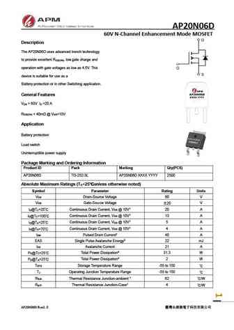
ap20n06d.pdf
AP20N06D 60V N-Channel Enhancement Mode MOSFET Description The AP20N06D uses advanced trench technology to provide excellent R , low gate charge and DS(ON) operation with gate voltages as low as 4.5V. This device is suitable for use as a Battery protection or in other Switching application. General Features V = 60V I =20 A DS D R
ap20n06bd.pdf
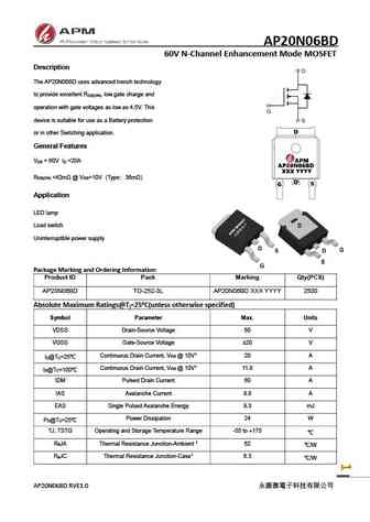
AP20N06BD 60V N-Channel Enhancement Mode MOSFET Description The AP20N06BD uses advanced trench technology to provide excellent R , low gate charge and DS(ON) operation with gate voltages as low as 4.5V. This device is suitable for use as a Battery protection or in other Switching application. General Features V = 60V I =20A DS D R

ap120n06p ap120n06t.pdf
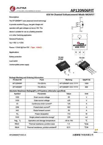
AP120N06PIT 65V N-Channel Enhancement Mode MOSFET Description The AP120N06P/T uses advanced trench technology to provide excellent R , low gate charge and DS(ON) operation with gate voltages as low as 10V. This device is suitable for use as a Battery protection or in other Switching application. General Features V = 65V I =125A DS D R
apg20n06s.pdf
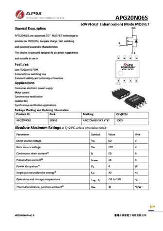
APG20N06S 60V N-SGT Enhancement Mode MOSFET General Description APG20N06S use advanced SGT MOSFET technology to provide low RDS(ON), low gate charge, fast switching and excellent avalanche characteristics. This device is specially designed to get better ruggedness and suitable to use in Features Low RDS(on) & FOM Extremely low switching loss Excellent stability and unifor
Другие MOSFET... SI2314 , SI2315 , SI2319 , SI2323 , SI2328 , SIA519 , XP151A13AO , XP152A12CO , 75N75 , 60N03 , 70N03 , 90N03 , SSS10N60 , SSS12N60 , SSS1N60 , SSS2N60 , SSS5N60 .
History: APQ07SN80BF | APQ08SN50BH | SM6019NSF
History: APQ07SN80BF | APQ08SN50BH | SM6019NSF
🌐 : EN ES РУ

Список транзисторов
Обновления
MOSFET: ASU70R600E | ASU65R850E | ASU65R550E | ASU65R350E | ASR65R120EFD | ASR65R046EFD | ASQ65R046EFD | ASM65R280E | ASM60R330E | ASE70R950E | ASD80R750E | ASD70R950E | ASD70R600E | ASD70R380E | ASD65R850E | ASD65R550E
Popular searches
se9302 transistor | fr5305 datasheet | y2 transistor | 40n06 | bc108b | oc84 | c6090 | ksa1015yta