90N03 datasheet, аналоги, основные параметры
Наименование производителя: 90N03 📄📄
Тип транзистора: MOSFET
Полярность: N
Предельные значения
Pd ⓘ - Максимальная рассеиваемая мощность: 95 W
|Vds|ⓘ - Максимально допустимое напряжение сток-исток: 30 V
|Vgs|ⓘ - Максимально допустимое напряжение затвор-исток: 20 V
|Id| ⓘ - Максимально допустимый постоянный ток стока: 90 A
Tj ⓘ - Максимальная температура канала: 175 °C
Электрические характеристики
RDSonⓘ - Сопротивление сток-исток открытого транзистора: 0.006 Ohm
Тип корпуса: TO251
📄📄 Копировать
Аналог (замена) для 90N03
- подборⓘ MOSFET транзистора по параметрам
90N03 даташит
90n03.pdf
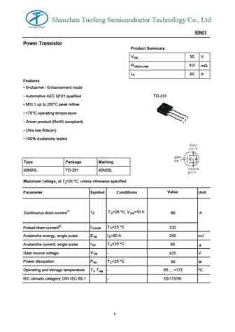
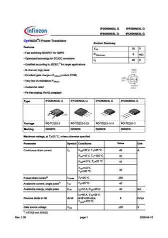
Shenzhen Tuofeng Semiconductor Technology Co., Ltd 90N03 Power-Transistor Product Summary V 30 V DS R 6.0 m DS(on),max I 80 A D Features N-channel - Enhancement mode Automotive AEC Q101 qualified TO-251 MSL1 up to 260 C peak reflow 175 C operating temperature 3 2 Green product (RoHS compliant) 1 Ultra low Rds(on) 100% Avalanche tested Typ
ipd090n03lg ipf090n03lg ips090n03lg ipu090n03lg.pdf
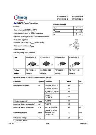
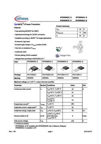
Type IPD090N03L G IPF090N03L G IPS090N03L G IPU090N03L G OptiMOS 3 Power-Transistor Product Summary Features V 30 V DS Fast switching MOSFET for SMPS R 9 m DS(on),max Optimized technology for DC/DC converters I 40 A D Qualified according to JEDEC1) for target applications N-channel, logic level Excellent gate charge x R product (FOM) DS(on) Very low
std90n03l std90n03l-1.pdf
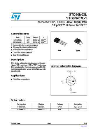
STD90N03L STD90N03L-1 N-channel 30V - 0.005 - 80A - DPAK/IPAK STripFET III Power MOSFET General features Type VDSS RDS(on) ID STD90N03L 30V 0.0057 80A (1) STD90N03L-1 30V 0.0057 80A (1) 3 3 2 1 1. Pulse width limited by safe operating area 1 RDS(on)*Qg industry s benchmark Conduction losses reduced IPAK DPAK Switching losses reduced Low threshold
np90n03vlg.pdf
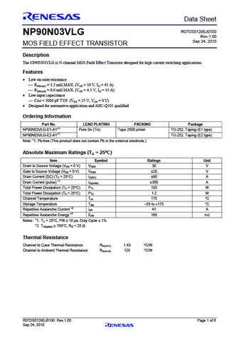
Preliminary Data Sheet R07DS0129EJ0100 NP90N03VLG Rev.1.00 Sep 24, 2010 MOS FIELD EFFECT TRANSISTOR Description The NP90N03VLG is N-channel MOS Field Effect Transistor designed for high current switching applications. Features Low on-state resistance RDS(on)1 = 3.2 m MAX. (VGS = 10 V, ID = 45 A) RDS(on)2 = 8.0 m MAX. (VGS = 4.5 V, ID = 35 A) Low input c
np90n03vug.pdf
To our customers, Old Company Name in Catalogs and Other Documents On April 1st, 2010, NEC Electronics Corporation merged with Renesas Technology Corporation, and Renesas Electronics Corporation took over all the business of both companies. Therefore, although the old company name remains in this document, it is a valid Renesas Electronics document. We appreciate your understanding.
np90n03vhg.pdf
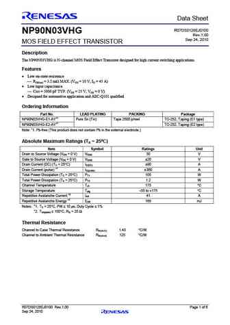
Preliminary Data Sheet R07DS0128EJ0100 NP90N03VHG Rev.1.00 Sep 24, 2010 MOS FIELD EFFECT TRANSISTOR Description The NP90N03VHG is N-channel MOS Field Effect Transistor designed for high current switching applications. Features Low on-state resistance RDS(on) = 3.2 m MAX. (VGS = 10 V, ID = 45 A) Low input capacitance Ciss = 5000 pF TYP. (VDS = 25 V, VGS =
rss090n03fu6tb.pdf
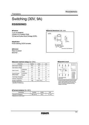
RSS090N03 Transistors Switching (30V, 9A) RSS090N03 External dimensions (Unit mm) Features 1) Low on-resistance. SOP8 5.0 0.2 2) Built-in G-S Protection Diode. 3) Small and Surface Mount Package (SOP8). 0.2 0.1 Application Power switching, DC/DC converter. 0.4 0.1 1.27 0.1 Each lead has same dimensions Structure Silicon N-channel MOS FET Equivalent c
rsh090n03tb1.pdf
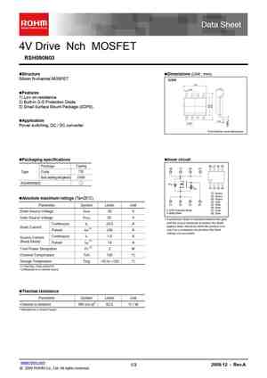
4V Drive Nch MOSFET RSH090N03 Structure Dimensions (Unit mm) Silicon N-channel MOSFET SOP8 Features 1) Low on-resistance. 2) Built-in G-S Protection Diode. 3) Small Surface Mount Package (SOP8). Application Power switching, DC / DC converter. Each lead has same dimensions Packaging specifications Inner circuit (8) (7) (6) (5) Package Taping (8) (7)
rxh090n03.pdf
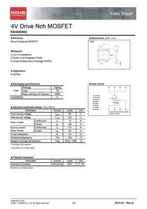
Data Sheet 4V Drive Nch MOSFET RXH090N03 Structure Dimensions (Unit mm) Silicon N-channel MOSFET SOP8 (8) (5) Features 1) Low on-resistance. 2) Built-in G-S Protection Diode. (1) (4) 3) Small Surface Mount Package (SOP8). Application Switching Packaging specifications Inner circuit (8) (7) (6) (5) Package Taping Type Code TB Basic ordering unit (pieces
sup90n03.pdf
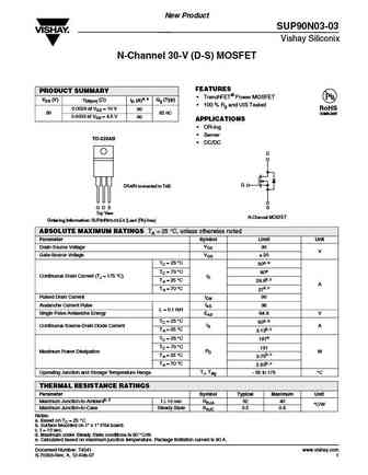
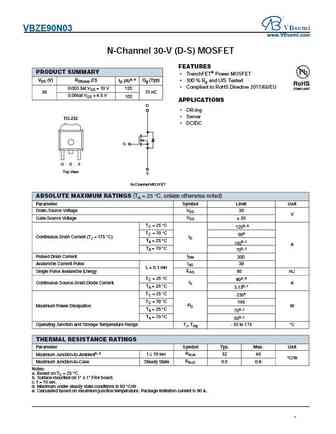
New Product SUP90N03-03 Vishay Siliconix N-Channel 30-V (D-S) MOSFET FEATURES PRODUCT SUMMARY TrenchFET Power MOSFET VDS (V) rDS(on) ( ) ID (A)a, e Qg (Typ) 100 % Rg and UIS Tested 0.0029 at VGS = 10 V 90 RoHS 30 82 nC COMPLIANT 0.0033 at VGS = 4.5 V 90 APPLICATIONS OR-ing Server TO-220AB DC/DC D G DRAIN connected to TAB G D S S Top View
sup90n03-03.pdf
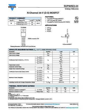
SUP90N03-03 Vishay Siliconix N-Channel 30-V (D-S) MOSFET FEATURES PRODUCT SUMMARY TrenchFET Power MOSFET VDS (V) RDS(on) ( ) ID (A)a, e Qg (Typ) 100 % Rg and UIS Tested Compliant to RoHS Directive 2011/65/EU 0.0029 at VGS = 10 V 90 30 82 nC 0.0033 at VGS = 4.5 V 90 APPLICATIONS TO-220AB OR-ing D Server DC/DC G DRAIN connected to TAB S G
sum90n03.pdf
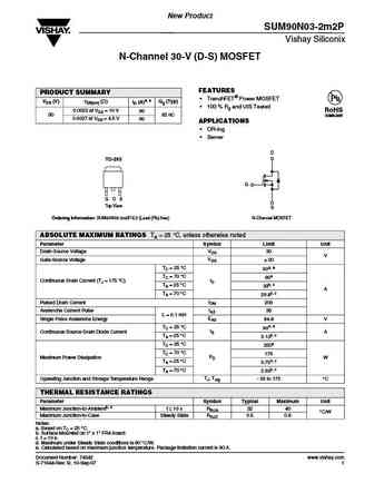
New Product SUM90N03-2m2P Vishay Siliconix N-Channel 30-V (D-S) MOSFET FEATURES PRODUCT SUMMARY TrenchFET Power MOSFET VDS (V) rDS(on) ( ) ID (A)a, e Qg (Typ) 100 % Rg and UIS Tested 0.0022 at VGS = 10 V 90 RoHS 30 82 nC COMPLIANT 0.0027 at VGS = 4.5 V 90 APPLICATIONS OR-ing Server D TO-263 G G D S Top View S Ordering Information SUM90N03-2m
sum90n03-2m2p.pdf
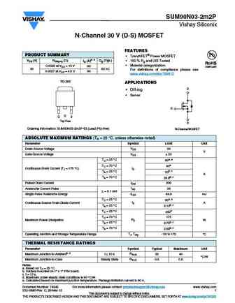
SUM90N03-2m2P Vishay Siliconix N-Channel 30 V (D-S) MOSFET FEATURES PRODUCT SUMMARY TrenchFET Power MOSFET VDS (V) RDS(on) ( ) ID (A)a, e Qg (Typ.) 100 % Rg and UIS Tested Material categorization 0.0022 at VGS = 10 V 90 30 82 nC For definitions of compliance please see 0.0027 at VGS = 4.5 V 90 www.vishay.com/doc?99912 TO-263 APPLICATIONS D OR-ing
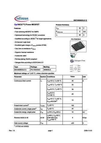
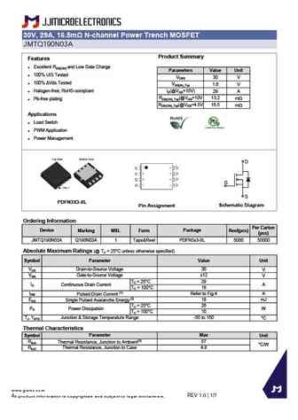
bsc090n03lsg.pdf
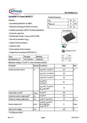
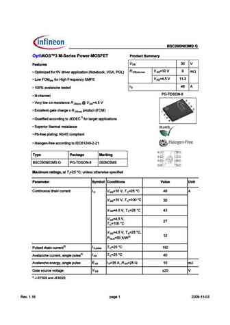
BSC090N03LS G OptiMOS 3 Power-MOSFET Product Summary Features VDS 30 V Fast switching MOSFET for SMPS RDS(on),max 9 mW Optimized technology for DC/DC converters ID 48 A Qualified according to JEDEC1) for target applications PG-TDSON-8 N-channel; Logic level Excellent gate charge x R product (FOM) DS(on) Very low on-resistance R DS(on) Superio
ips090n03l.pdf
pe % # ! % # ! %' # ! %) # ! % (>.;?6?@ %>E Features D S !4EF EI
ipd090n03lg6.pdf
pe % # ! % # ! %' # ! %) # ! % (>.;?6?@ %>E Features D R 3DE DH;E5 ;@9 ') - . 8AC -'*- m D n) m x R ) BE;?;K76 E75 @A>A9J 8AC 5A@G7CE7CD 4 D 1) R + F3>;8;76 355AC6;@9 EA $ 8AC E3C97E 3BB>;53E;A@D R ( 5 3@@7> >A9;5 >7G7> R I57>>7@E 93E7 5 3C97 I BCA6F5E ) ' D n) R 07CJ >AH A@ C7D;DE3@57 D n) R G3>3@5 7 C3E76 R *4 8C77 B>3E;@9 , A"- 5A?B>;3@E
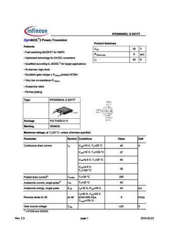
ipd090n03lge8177.pdf

Type IPD090N03L G E8177 OptiMOS 3 Power-Transistor Product Summary Features VDS 30 V Fast switching MOSFET for SMPS RDS(on),max 9 mW Optimized technology for DC/DC converters ID 40 A Qualified according to JEDEC1) for target applications N-channel, logic level Excellent gate charge x R product (FOM) DS(on) Very low on-resistance R DS(on) Aval
ipd90n03s4l-03 ipd90n03s4l-03 ds.pdf
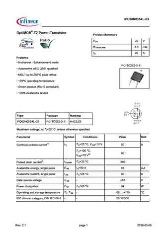
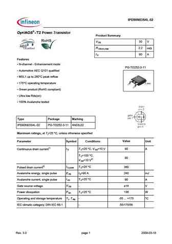
IPD90N03S4L-03 OptiMOS -T2 Power-Transistor Product Summary V 30 V DS R 3.3 m DS(on),max I 90 A D Features N-channel - Enhancement mode PG-TO252-3-11 Automotive AEC Q101 qualified MSL1 up to 260 C peak reflow 175 C operating temperature Green product (RoHS compliant) 100% Avalanche tested Type Package Marking IPD90N03S4L-03 PG-TO252-3-11 4N03L03
ipd090n03lg .pdf
pe $ " $;B1= '=- >5>?;= $=;0@/? &@99-=D Features D Q 2CD CG D49 ?8 ') - . 7@B -'*- m D n) m x Q ) AD > J65 D649?@=@8I 7@B 4@?F6BD6BC 4 D 1) Q + E2= 7 65 244@B5 ?8 D@ $ 7@B D2B86D 2AA= 42D @?C Q ( 492??6= =@8 4 =6F6= Q H46==6?D 82D6 492B86 H AB@5E4D ) ' D n) Q /6BI =@G @? B6C CD2?46 D n) Q F2=2?496 B2D65 Q *3 7B66 A=2D ?8 Type #* ( & ! Package G O 11 M
bsc090n03ls.pdf
& " & E $;B1= !#& ' $=;0@/? &@99-=D Features D Q 2CD CG D49 ?8 ') - . 7@B -'*- m D n) m x 4 Q ) AD > J65 D649?@=@8I 7@B 4@?F6BD6BC D 1) Q + E2= 7 65 244@B5 ?8 D@ $ 7@B D2B86D 2AA= 42D @?C G D ON Q ( 492??6= &@8 4 =6F6= Q H46==6?D 82D6 492B86 H AB@5E4D ) ' D n) Q /6BI =@G @? B6C CD2?46 D n) Q -EA6B @B D96B>2= B6C CD2?46 Q F2=2?496 B2D65 Q *3 7B66 A=2D ?8 , @"
bsc090n03msg.pdf
% ! % D %0 S 07DK >AI A@ D7E;EF3@57 0 D n) G S J57>>7@F 93F7 5 3D97 J BDA6G5F !* ( D n) 1) S , G3>;8;76 355AD6;@9 FA % 8AD F3D97F 3BB>;53F;A@E S .GB7D;AD F 7D
ipd090n03l.pdf
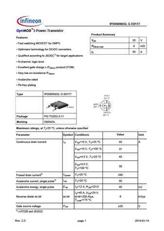
Type IPD090N03L G E8177 OptiMOS 3 Power-Transistor Product Summary Features VDS 30 V Fast switching MOSFET for SMPS RDS(on),max 9 mW Optimized technology for DC/DC converters ID 40 A Qualified according to JEDEC1) for target applications N-channel, logic level Excellent gate charge x R product (FOM) DS(on) Very low on-resistance R DS(on) Aval
ipd090n03lg9.pdf

pe % # ! % # ! %' # ! %) # ! % (>.;?6?@ %>E Features D S !4EF EI
ipd90n03s4l-02 ipd90n03s4l-02 ds 3 0.pdf
IPD90N03S4L-02 OptiMOS -T2 Power-Transistor Product Summary V 30 V DS R 2.2 m DS(on),max I 90 A D Features N-channel - Enhancement mode PG-TO252-3-11 Automotive AEC Q101 qualified MSL1 up to 260 C peak reflow 175 C operating temperature Green product (RoHS compliant) Ultra low Rds(on) 100% Avalanche tested Type Package Marking IPD90N03S4L-02
ut90n03.pdf
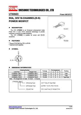
UNISONIC TECHNOLOGIES CO., LTD UT90N03 Power MOSFET 90A, 30V N-CHANNEL(D-S) POWER MOSFET DESCRIPTION The UTC UT90N03 is an N-channel enhancement mode Power FET, it uses UTC s advanced technology to provide customers a minimum on-state resistance. The UTC UT90N03 is suitable for server and DC-DC converters. FEATURES * RDS(ON)=2.4m @ VGS=10V, ID=28.8A * Improv
am90n03-26p.pdf

Analog Power AM90N03-26P N-Channel 30-V (D-S) MOSFET These miniature surface mount MOSFETs utilize a PRODUCT SUMMARY high cell density trench process to provide low VDS (V) rDS(on) m( ) ID (A) rDS(on) and to ensure minimal power loss and heat dissipation. Typical applications are DC-DC 26 @ VGS = 10V converters and power management in portable and 30 88a 40 @ VGS = 4.5V batter
am90n03-03p.pdf
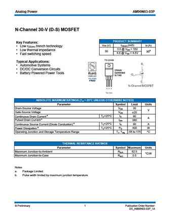
Analog Power AM90N03-03P N-Channel 30-V (D-S) MOSFET PRODUCT SUMMARY Key Features rDS(on) (m ) VDS (V) ID (A) Low r trench technology DS(on) 3.5 @ VGS = 10V Low thermal impedance 30 90a 4.6 @ VGS = 4.5V Fast switching speed Typical Applications Automotive Systems DC/DC Conversion Circuits DRAIN connected Battery Powered Power Tools to TAB
am90n03-08p.pdf
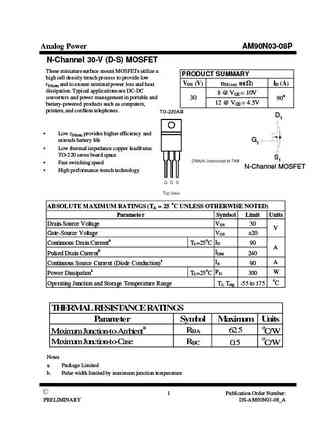
Analog Power AM90N03-08P N-Channel 30-V (D-S) MOSFET These miniature surface mount MOSFETs utilize a PRODUCT SUMMARY high cell density trench process to provide low VDS (V) rDS(on) m( ) ID (A) rDS(on) and to ensure minimal power loss and heat dissipation. Typical applications are DC-DC 8 @ VGS = 10V converters and power management in portable and 30 90a 12 @ VGS = 4.5V battery
am90n03-01p.pdf
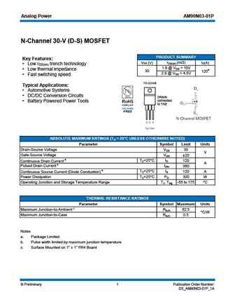
Analog Power AM90N03-01P N-Channel 30-V (D-S) MOSFET PRODUCT SUMMARY Key Features rDS(on) (m ) VDS (V) ID(A) Low r trench technology DS(on) 1.9 @ VGS = 10V Low thermal impedance 30 120a 2.9 @ VGS = 4.5V Fast switching speed Typical Applications Automotive Systems DC/DC Conversion Circuits DRAIN connected Battery Powered Power Tools to TAB
am90n03-04d.pdf
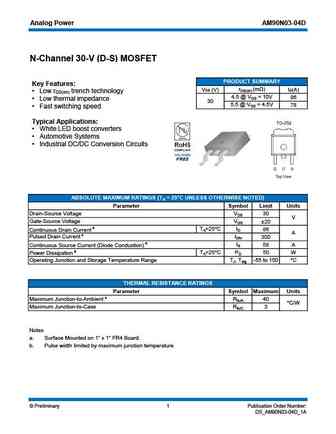
Analog Power AM90N03-04D N-Channel 30-V (D-S) MOSFET PRODUCT SUMMARY Key Features rDS(on) (m ) VDS (V) ID(A) Low r trench technology DS(on) 4.5 @ VGS = 10V 86 Low thermal impedance 30 5.5 @ VGS = 4.5V 78 Fast switching speed Typical Applications White LED boost converters Automotive Systems Industrial DC/DC Conversion Circuits ABSOLUTE MAXIM
am90n03-04i.pdf

Analog Power AM90N03-04I N-Channel 30-V (D-S) MOSFET These miniature surface mount MOSFETs utilize a PRODUCT SUMMARY high cell density trench process to provide low VDS (V) rDS(on) m( ) ID (A) rDS(on) and to ensure minimal power loss and heat dissipation. Typical applications are DC-DC 4.5 @ VGS = 10V 87 converters and power management in portable and 30 5.5 @ VGS = 4.5V 78 bat
am90n03-06b.pdf
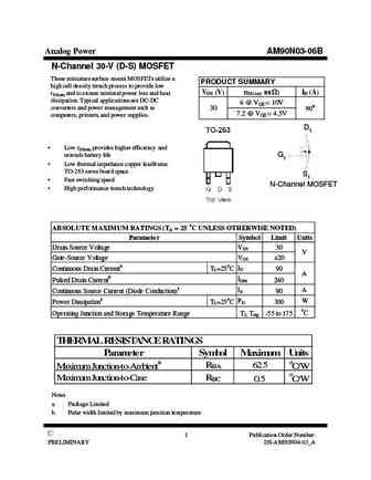
Analog Power AM90N03-06B N-Channel 30-V (D-S) MOSFET These miniature surface mount MOSFETs utilize a PRODUCT SUMMARY high cell density trench process to provide low VDS (V) rDS(on) m( ) ID (A) rDS(on) and to ensure minimal power loss and heat dissipation. Typical applications are DC-DC 6 @ VGS = 10V converters and power management such as 30 90a 7.2 @ VGS = 4.5V computers, pri
am90n03-03b.pdf
Analog Power AM90N03-03B N-Channel 30-V (D-S) MOSFET PRODUCT SUMMARY Key Features rDS(on) (m ) VDS (V) ID(A) Low r trench technology DS(on) 3.8 @ VGS = 10V Low thermal impedance 30 90a 4.6 @ VGS = 4.5V Fast switching speed Typical Applications White LED boost converters Automotive Systems Industrial DC/DC Conversion Circuits ABSOLUTE MAXIMUM
am90n03-02d.pdf

Analog Power AM90N03-02D N-Channel 30-V (D-S) MOSFET PRODUCT SUMMARY These miniature surface mount MOSFETs utilize a high cell density trench process to provide low VDS (V) rDS(on) m( ) ID (A) rDS(on) and to ensure minimal power loss and heat 2 @ VGS = 10V 130 dissipation. Typical applications are DC-DC 30 converters and power management in portable and 3.2 @ VGS = 4.5V 103 bat
mta90n03zn3.pdf
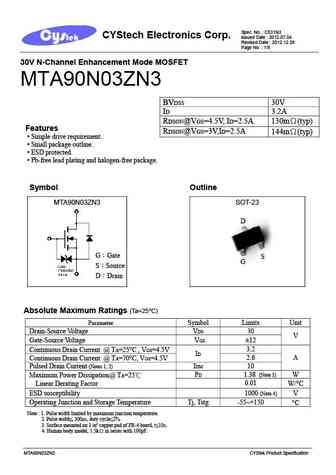
Spec. No. C831N3 CYStech Electronics Corp. Issued Date 2012.07.04 Revised Date 2012.12.28 Page No. 1/8 30V N-Channel Enhancement Mode MOSFET MTA90N03ZN3 BVDSS 30V ID 3.2A RDSON@VGS=4.5V, ID=2.5A 130m (typ) Features RDSON@VGS=3V,ID=2.5A 144m (typ) Simple drive requirement. Small package outline. ESD protected. Pb-free lead plating and halogen-
cs90n03 b4.pdf

Silicon N-Channel Power MOSFET R CS90N03 B4 General Description VDSS 25 V CS90N03 B4, the silicon N-channel Enhanced ID 90 A PD(TC=25 ) 80 W VDMOSFETs, is obtained by the self-aligned planar RDS(ON)Typ 4.8 m Technology which reduce the conduction loss, improve switching performance and enhance the avalanche energy. The transistor can be used in various powe
cs90n03 b3.pdf

Silicon N-Channel Power MOSFET R CS90N03 B3 General Description VDSS 25 V CS90N03 B3, the silicon N-channel Enhanced ID 90 A PD(TC=25 ) 80 W VDMOSFETs, is obtained by the self-aligned planar RDS(ON)Typ 4.8 m Technology which reduce the conduction loss, improve switching performance and enhance the avalanche energy. The transistor can be used in various power s
dhb90n03b17 dhd90n03b17.pdf
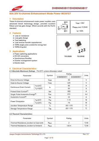
DHB90N03B17/DHD90N03B17 90A 30V N-channel Enhancement Mode Power MOSFET 1 Description These N-channel enhancement mode power mosfets used 2 D V = 30V DSS advanced trench technology design, provided excellent Rdson and low gate charge. Which accords with the RoHS G R = 4.0m DS(on) (TYP) standard. 1 3 S I = 90A D 2 Features Low on resistance Low gate charge Fast
ndt90n03.pdf
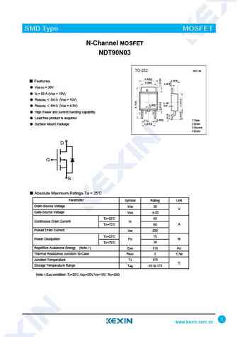
SMD Type MOSFET N-Channel MOSFET NDT90N03 TO-252 Unit mm +0.15 6.50-0.15 +0.1 2.30 -0.1 Features +0.2 5.30-0.2 +0.8 0.50 -0.7 VDS (V) = 30V 4 ID = 85 A (VGS = 10V) RDS(ON) 5m (VGS = 10V) 0.127 +0.1 0.80-0.1 max RDS(ON) 8m (VGS = 4.5V) High Power and current handing capability Lead free product is acquired + 0.1 2.3 0.60- 0.
sld90n03tb.pdf
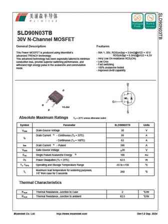
SLD90N03TB 30V N-Channel MOSFET General Description Features This Power MOSFET is produced using Msemitek s - 99A 1), 30V, RDS(on)typ = 3.6m @VGS = 10 V RDS(on)typ = 6.5m @VGS = 4.5V advanced TRENCH technology. This advanced technology has been especially tailored to minimize - Very Low On-resistance RDS(ON) - Low Crss conduction loss, provide superior switching performance, and -
me90n03 me90n03-g.pdf

ME90N03/ME90N03-G N-Channel 30V(D-S) MOSFET, ESD Protected GENERAL DESCRIPTION FEATURES The ME90N03 is the N-Channel logic enhancement mode power RDS(ON) 4.8m @VGS=10V field effect transistors are produced using high cell density , DMOS RDS(ON) 9m @VGS=4.5V trench technology. This high density process is especially tailored to ESD Protected minimize on-state resis
hrlfs190n03k.pdf
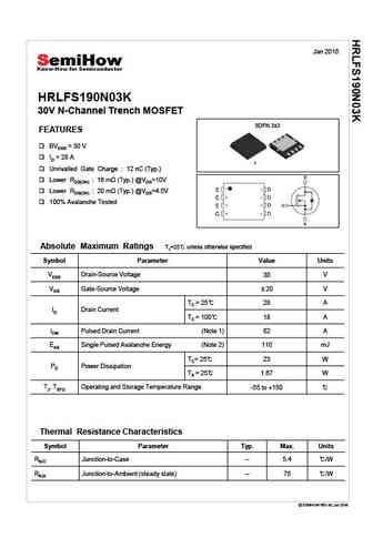
Jan 2016 HRLFS190N03K 30V N-Channel Trench MOSFET 8DFN 3x3 FEATURES BVDSS = 30 V ID = 28 A 1 Unrivalled Gate Charge 12 nC (Typ.) Lower RDS(ON) 16 (Typ.) @VGS=10V Lower RDS(ON) 20 (Typ.) @VGS=4.5V 100% Avalanche Tested Absolute Maximum Ratings TJ=25 unless otherwise specified Symbol Parameter Value Units VDSS Drain-Source Voltage 30 V VGS Gate-Source Voltage
hrlf190n03k.pdf
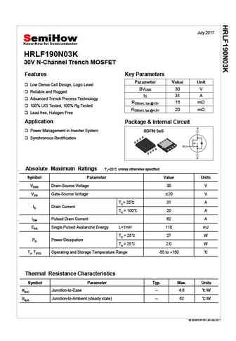
July 2017 HRLF190N03K 30V N-Channel Trench MOSFET Features Key Parameters Parameter Value Unit Low Dense Cell Design, Logic Level BVDSS 30 V Reliable and Rugged ID 31 A Advanced Trench Process Technology RDS(on), typ @10V 16 m 100% UIS Tested, 100% Rg Tested RDS(on), typ @4.5V 20 m Lead free, Halogen Free Application Package & Internal Circu
hrlfs90n03k.pdf

June 2017 HRLFS90N03K 30V N-Channel Trench MOSFET Features Key Parameters Parameter Value Unit Low Dense Cell Design, Logic Level BVDSS 30 V Reliable and Rugged ID 38 A Advanced Trench Process Technology RDS(on), typ @10V 9.0 m 100% UIS Tested, 100% Rg Tested RDS(on), typ @4.5V 13.0 m Lead free, Halogen Free Application Package & Internal Ci
sl90n03r.pdf
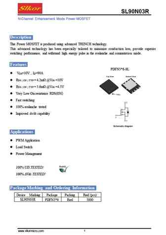
SL90N03R Description This Power MOSFET is produced using advanced TRENCH technology. This advanced technology has been especially tailored to minimize conduction loss, provide superior switching performance, and withstand high energy pulse in the avalanche and commutation mode. Features PDFN5*6-8L V =30V I =90A DS D R = 4.2m @V =10V DS ON TYP GS R =
wmk190n03ts.pdf
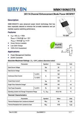
WMK190N03TS 30V N-Channel Enhancement Mode Power MOSFET Description WMK190N03TS uses advanced power trench technology that has been especially tailored to minimize the on-state resistance and yet maintain superior switching performance. Features S D G TO-220 V = 30V, I = 190A DS D R
wmm190n03ts.pdf
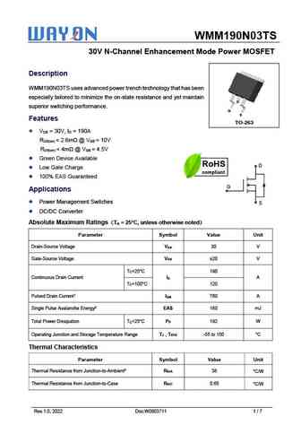
WMM190N03TS 30V N-Channel Enhancement Mode Power MOSFET Description WMM190N03TS uses advanced power trench technology that has been especially tailored to minimize the on-state resistance and yet maintain D superior switching performance. G S Features TO-263 V = 30V, I = 190A DS D R
wmo190n03ts.pdf
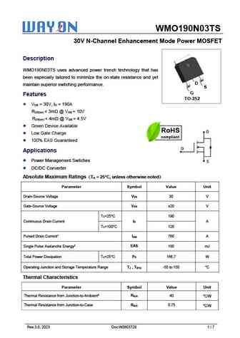
WMO190N03TS 30V N-Channel Enhancement Mode Power MOSFET Description WMO190N03TS uses advanced power trench technology that has been especially tailored to minimize the on-state resistance and yet D maintain superior switching performance. S G Features TO-252 V = 30V, I = 190A DS D R
cs90n03b4.pdf

Silicon N-Channel Power MOSFET R CS90N03 B4 General Description VDSS 25 V CS90N03 B4, the silicon N-channel Enhanced ID 90 A PD(TC=25 ) 80 W VDMOSFETs, is obtained by the self-aligned planar RDS(ON)Typ 4.8 m Technology which reduce the conduction loss, improve switching performance and enhance the avalanche energy. The transistor can be used in various powe
ad90n03s.pdf
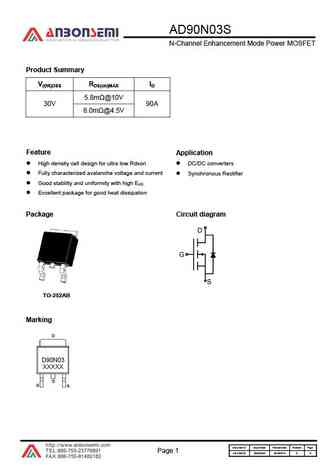
AD90N03S N-Channel Enhancement Mode Power MOSFET Product Summary V(BR)DSS RDS(on)MAX ID 5.8m @10V 30V 90A 8.0m @4.5V Feature Application High density cell design for ultra low Rdson DC/DC converters Fully characterized avalanche voltage and current Synchronous Rectifier Good stability and uniformity with high EAS Excellent package for good heat dissipation Package
hsh190n03.pdf
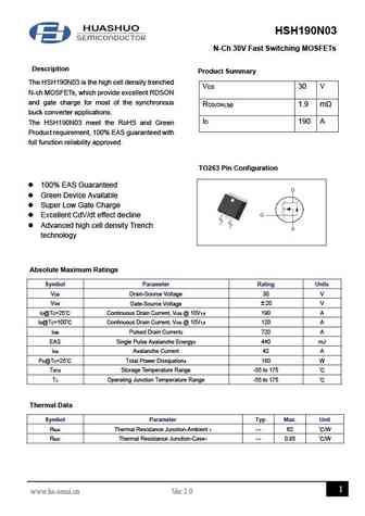
HSH190N03 N-Ch 30V Fast Switching MOSFETs Description Product Summary The HSH190N03 is the high cell density trenched VDS 30 V N-ch MOSFETs, which provide excellent RDSON and gate charge for most of the synchronous RDS(ON),typ 1.9 m buck converter applications. ID 190 A The HSH190N03 meet the RoHS and Green Product requirement, 100% EAS guaranteed with full function
hsu90n03.pdf
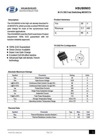
HSU90N03 N-Ch 30V Fast Switching MOSFETs Description Product Summary The HSU90N03 is the high cell density trenched N- VDS 30 V ch MOSFETs, which provide excellent RDSON and RDS(ON),typ 3.7 m gate charge for most of the synchronous buck converter applications. ID 90 A The HSU90N03 meet the RoHS and Green Product requirement 100% EAS guaranteed with full function reliabi
htd090n03.pdf
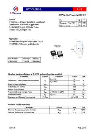
HTD090N03 P-1 30V N-Ch Power MOSFET Feature 30 V VDS High Speed Power Switching, Logic Level 7.5 RDS(on),typ VGS=10V m Enhanced Avalanche Ruggedness 50 A ID (Sillicon Limited) 100% UIS Tested, 100% Rg Tested Lead Free, Halogen Free Application Hard Switching and High Speed Circuit Drain DC/DC in Telecoms and Inductrial TO-252 Gate 2 Src 3 1 Part
90n03l.pdf
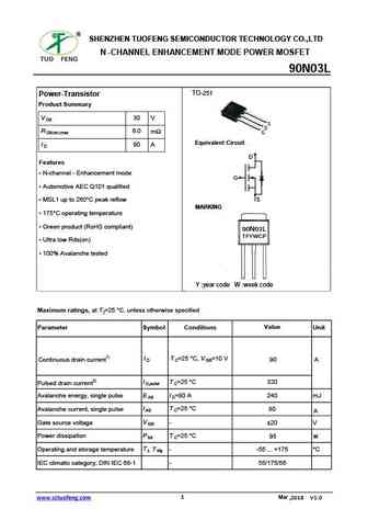
SHENZHEN TUOFENG SEMICONDUCTOR TECHNOLOGY CO.,LTD N -CHANNEL ENHANCEMENT MODE POWER MOSFET 90N03L TO-251 Power-Transistor Product Summary V 30 V DS S D R 6.0 m DS(on),max G Equivalent Circuit I 90 A D D Features N-channel - Enhancement mode G Automotive AEC Q101 qualified S MSL1 up to 260 C peak reflow MARKING 175 C operating temperature Green
vbze90n03.pdf
VBZE90N03 www.VBsemi.com N-Channel 30-V (D-S) MOSFET FEATURES PRODUCT SUMMARY TrenchFET Power MOSFET VDS (V) RDS(on) ( ) ID (A)a, e Qg (Typ) 100 % Rg and UIS Tested Compliant to RoHS Directive 2011/65/EU 0.003.8at VGS = 10 V 120 30 70 nC 0.006at VGS = 4.5 V 100 APPLICATIONS D OR-ing Server TO-252 DC/DC G G D S Top View S N-Channel MOSFET A
ttd90n03at ttp90n03at.pdf
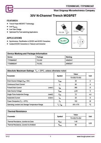
TTD90N03AT, TTP90N03AT Wuxi Unigroup Microelectronics Company Wuxi Unigroup Microelectronics Company 30V N-Channel Trench MOSFET FEATURES Trench Power MOSFET Technology Low RDS(ON) Low Gate Charge Optimized For Fast-switching Applications APPLICATIONS Synchronous Rectification in DC/DC and AC/DC Converters Isolated DC/DC Converters in Telecom and In
bcd90n03.pdf
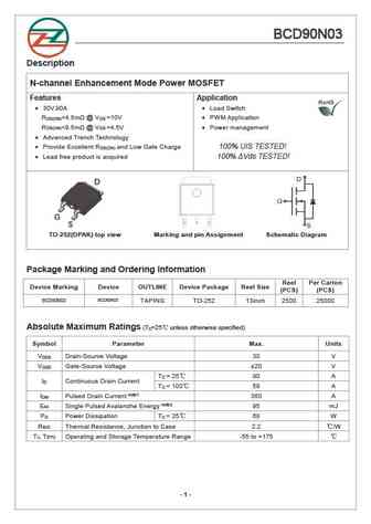
BCD90N03 Description N-channel Enhancement Mode Power MOSFET Features Application 30V,90A Load Switch R
ipd090n03l.pdf
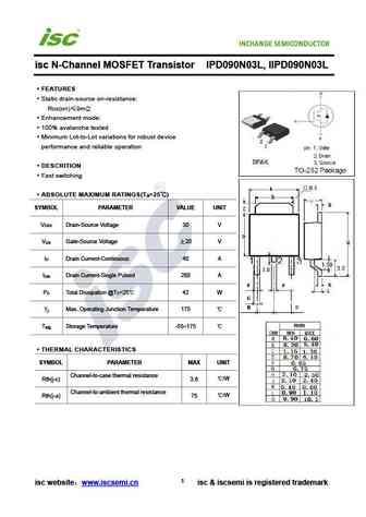
isc N-Channel MOSFET Transistor IPD090N03L, IIPD090N03L FEATURES Static drain-source on-resistance RDS(on) 9m Enhancement mode 100% avalanche tested Minimum Lot-to-Lot variations for robust device performance and reliable operation DESCRITION Fast switching ABSOLUTE MAXIMUM RATINGS(T =25 ) a SYMBOL PARAMETER VALUE UNIT V Drain-Source Voltage 30 V DSS V Ga
Другие IGBT... SI2323, SI2328, SIA519, XP151A13AO, XP152A12CO, 20N06, 60N03, 70N03, 2N60, SSS10N60, SSS12N60, SSS1N60, SSS2N60, SSS5N60, SSS7N60, SSS8N60, 1002
Параметры MOSFET. Взаимосвязь и компромиссы
History: BRCS080N10SHZC | PJ527BA | FDBL0200N100 | H07N60F | AP10G06S | APT1002RBN | FQPF6N40C
🌐 : EN ES РУ

Список транзисторов
Обновления
MOSFET: CS95118 | CS85105A | CS75N45 | CS72N12 | CS55N50 | CS48N75A | CS40N27 | MSQ60P04D | MSQ40P07D | MSQ30P40D | MSQ30P15 | MSQ30P07D | MSQ100N03D | MSHM60P14 | MSHM40N085 | MSHM30N46
Popular searches
40n06 | bc108b | oc84 | c6090 | ksa1015yta | 2n4240 | 2n5210 transistor | toshiba 2sc2290