3401. Аналоги и основные параметры
Наименование производителя: 3401
Тип транзистора: MOSFET
Полярность: P
Предельные значения
Pd ⓘ - Максимальная рассеиваемая мощность: 1.2 W
|Vds|ⓘ - Максимально допустимое напряжение сток-исток: 30 V
|Vgs|ⓘ - Максимально допустимое напряжение затвор-исток: 20 V
|Id| ⓘ - Максимально допустимый постоянный ток стока: 4.2 A
Tj ⓘ - Максимальная температура канала: 150 °C
Электрические характеристики
tr ⓘ - Время нарастания: 3 ns
Cossⓘ - Выходная емкость: 115 pf
RDSonⓘ - Сопротивление сток-исток открытого транзистора: 0.055 Ohm
Тип корпуса: SOT23
Аналог (замена) для 3401
- подборⓘ MOSFET транзистора по параметрам
3401 даташит
3401.pdf
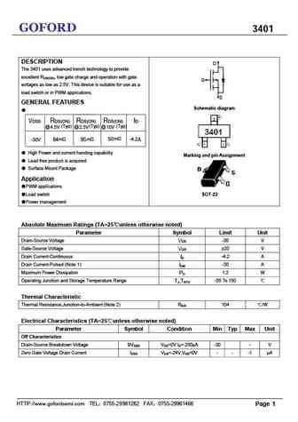
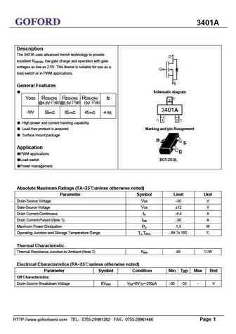
GOFORD 3401 DESCRIPTION D The 3401 uses advanced trench technology to provide excellent RDS(ON), low gate charge and operation with gate G voltages as low as 2.5V. This device is suitable for use as a load switch or in PWM applications. S GENERAL FEATURES Schematic diagram VDSS RDS(ON) RDS(ON) RDS(ON) ID @ 4.5V (Typ) @ 2.5V (Typ) @ 10V (Typ) m m m 50 -4.2
3401.pdf
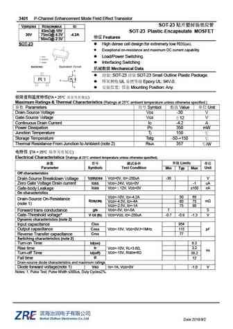
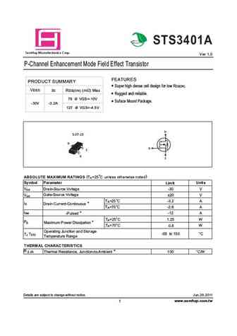
3401 P-Channel Enhancement Mode Field Effect Transistor SOT-23 V(BR)DSS RDS(ON)MAX ID 65m @-10V SOT-23 Plastic-Encapsulate MOSFET 30V 75m @-4.5V -4.2A Features 90m @-2.5V SOT-23 High dense cell design for extremely low RDS(on). Exceptional on-resistance and maximum DC current capability. Load/Power Switching. Interfacing
nce3401ay.pdf
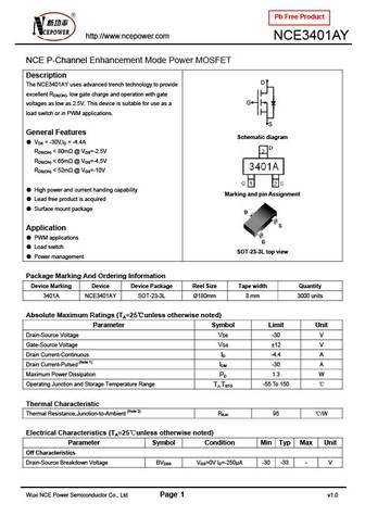
Pb Free Product http //www.ncepower.com NCE3401AY NCE P-Channel Enhancement Mode Power MOSFET Description D The NCE3401AY uses advanced trench technology to provide excellent RDS(ON), low gate charge and operation with gate G voltages as low as 2.5V. This device is suitable for use as a load switch or in PWM applications. S General Features Schematic diagram VDS = -30
mch3401.pdf
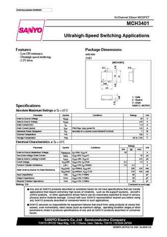
Ordering number ENN6443 N-Channel Silicon MOSFET MCH3401 Ultrahigh-Speed Switching Applications Features Package Dimensions Low ON resistance. unit mm Ultrahigh-speed swithcing. 2167 2.5V drive. [MCH3401] 0.3 0.15 3 1 2 0.65 2.0 1 Gate 2 Source 3 Drain SANYO MCPH3 Specifications Absolute Maximum Ratings at Ta = 25 C Parameter Symbol Conditions Ratings
ne34018.pdf
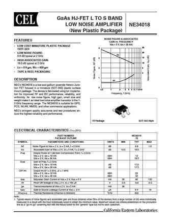
GaAs HJ-FET L TO S BAND LOW NOISE AMPLIFIER NE34018 (New Plastic Package) NOISE FIGURE & ASSOCIATED FEATURES GAIN vs. FREQUENCY VDS = 3 V, IDS = 20 mA LOW COST MINIATURE PLASTIC PACKAGE 25 25 4 4 (SOT-343) 20 20 LOW NOISE FIGURE GA 0.6 dB typical at 2 GHz 15 15 3 3 HIGH ASSOCIATED GAIN 10 10 16.0 dB typical at 2 GHz LG = 0.6 2 5 m, WG
dmg3401lsn.pdf
DMG3401LSN 30V P-CHANNEL ENHANCEMENT MODE MOSFET Product Summary Features Low Input Capacitance ID V(BR)DSS RDS(on) max Low On-Resistance TA = 25 C Low Input/Output Leakage 50m @ VGS = -10V -3.7A Totally Lead-Free & Fully RoHS Compliant (Notes 1 & 2) -30V 60m @ VGS = -4.5V -3.3A Halogen and Antimony Free. Green Device (Note 3) 85m @ VGS =
ut3401.pdf
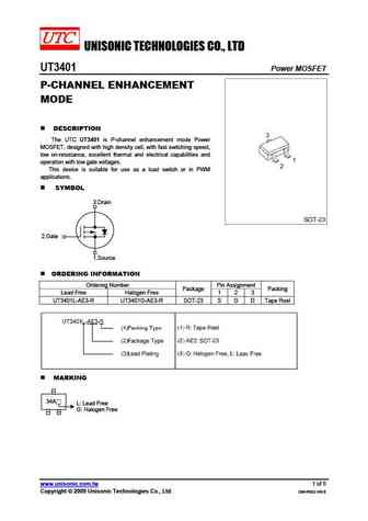
UNISONIC TECHNOLOGIES CO., LTD UT3401 Power MOSFET P-CHANNEL ENHANCEMENT MODE DESCRIPTION The UTC UT3401 is P-channel enhancement mode Power MOSFET, designed with high density cell, with fast switching speed, low on-resistance, excellent thermal and electrical capabilities and operation with low gate voltages. This device is suitable for use as a load switch or in PWM appli
ut3401z.pdf
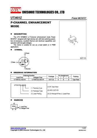
UNISONIC TECHNOLOGIES CO., LTD UT3401Z Power MOSFET P-CHANNEL ENHANCEMENT MODE DESCRIPTION The UTC UT3401Z is P-channel enhancement mode Power MOSFET, designed with high density cell, with fast switching speed, low on-resistance, excellent thermal and electrical capabilities and operation with low gate voltages. This device is suitable for use as a load switch or in PWM app
ut3401zl-ae3-r ut3401zg-ae3-r.pdf
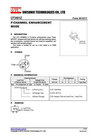
UNISONIC TECHNOLOGIES CO., LTD UT3401Z Power MOSFET P-CHANNEL ENHANCEMENT MODE DESCRIPTION The UTC UT3401Z is P-channel enhancement mode Power MOSFET, designed with high density cell, with fast switching speed, low on-resistance, excellent thermal and electrical capabilities and operation with low gate voltages. This device is suitable for use as a load switch or in PWM a
ut3401g-ae3-r.pdf
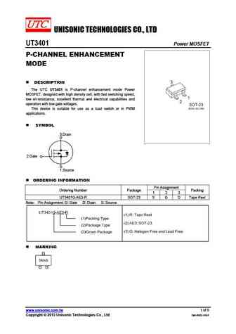
UNISONIC TECHNOLOGIES CO., LTD UT3401 Power MOSFET P-CHANNEL ENHANCEMENT MODE DESCRIPTION The UTC UT3401 is P-channel enhancement mode Power MOSFET, designed with high density cell, with fast switching speed, low on-resistance, excellent thermal and electrical capabilities and operation with low gate voltages. This device is suitable for use as a load switch or in PWM app
smg3401.pdf
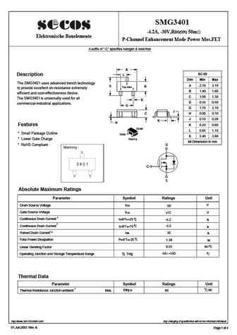
SMG3401 -4.2A, -30V,RDS(ON) 50m Elektronische Bauelemente P-Channel Enhancement Mode Power Mos.FET A suffix of "-C" specifies halogen & lead-free A SC-59 Description L Dim Min Max The SMG3401 uses advanced trench technology 3 A 2.70 3.10 S B Top View to provide excellent on-resistance extremely 2 1 B 1.40 1.60 efficient and cost-effectiveness device. C 1.00 1.30 The
tsm3401cx.pdf
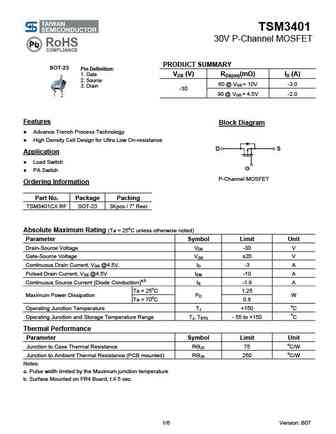
TSM3401 30V P-Channel MOSFET PRODUCT SUMMARY SOT-23 Pin Definition 1. Gate VDS (V) RDS(on)(m ) ID (A) 2. Source 60 @ VGS = 10V -3.0 3. Drain -30 90 @ VGS = 4.5V -2.0 Features Block Diagram Advance Trench Process Technology High Density Cell Design for Ultra Low On-resistance Application Load Switch PA Switch P-Channel MOSFET Ordering Info
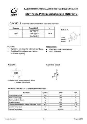
cjk3401ah.pdf
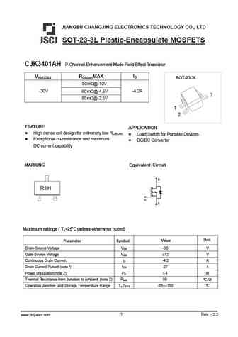
JIANGSU CHANGJING ELECTRONICS TECHNOLOGY CO., LTD SOT-23-3L Plastic-Encapsulate MOSFETS CJK3401AH P-Channel Enhancement Mode Field Effect Transistor ID V(BR)DSS RDS(on)MAX SOT-23-3L 50m @-10V -30V -4.2A 60 m @-4.5V m @-2.5V 85 FEATURE APPLICATION High dense cell design for extremely low RDS(ON) Load Switch for Portable Devices Exceptional on-resistance and maximum
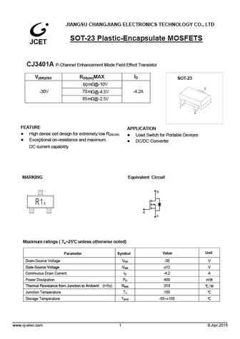
cj3401.pdf
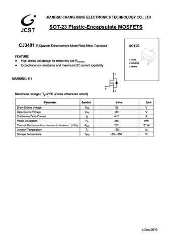
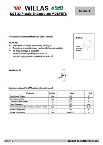
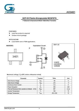
JIANGSU CHANGJIANG ELECTRONICS TECHNOLOGY CO., LTD SOT-23 Plastic-Encapsulate MOSFETS CJ3401 P-Channel Enhancement Mode Field Effect Transistor SOT-23 FEATURE 1. GATE High dense cell design for extremely low RDS(ON). 2. SOURCE Exceptional on-resistance and maximum DC current capability 3. DRAIN D MARKING R1 G S Maximum ratings ( Ta=25 unless otherwise noted
cjk3401a.pdf
JIANGSU CHANGJIANG ELECTRONICS TECHNOLOGY CO., LTD SOT-23-3L Plastic-Encapsulate MOSFETS CJK3401A P-Channel Enhancement Mode Field Effect Transistor ID V(BR)DSS RDS(on)MAX SOT-23-3L m @-10V 60 -30V 70 m -4.2A @-4.5V m @-2.5V 85 1. GATE 2. SOURCE 3. DRAIN D FEATURE APPLICATION High dense cell design for extremely low RDS(ON) Load Switch for Portable Devi
cj3401a.pdf
JIANGSU CHANGJIANG ELECTRONICS TECHNOLOGY CO., LTD SOT-23 Plastic-Encapsulate MOSFETS CJ3401A P-Channel Enhancement Mode Field Effect Transistor ID V(BR)DSS RDS(on)MAX SOT-23 m @-10V 60 -30V 70 m -4.2A @-4.5V m @-2.5V 85 FEATURE APPLICATION High dense cell design for extremely low RDS(ON) Load Switch for Portable Devices Exceptional on-resistance and maxi
cj3401-hf.pdf
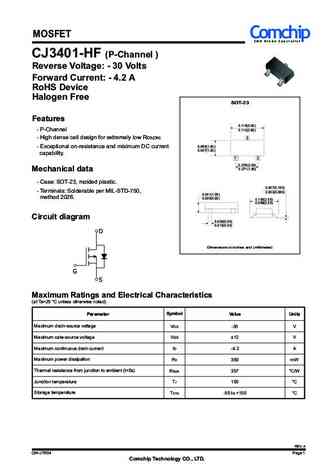
MOSFET Comchip S M D D i o d e S p e c i a l i s t CJ3401-HF (P-Channel ) Reverse Voltage - 30 Volts Forward Current - 4.2 A RoHS Device Halogen Free SOT-23 Features 0.118(3.00) - P-Channel 0.110(2.80) - High dense cell design for extremely low RDS(ON) 3 0.055(1.40) - Exceptional on-resistance and miximum DC current 0.047(1.20) capability. 1 2 0.079(2.00) 0.071(1.80) Me
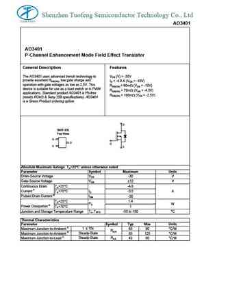
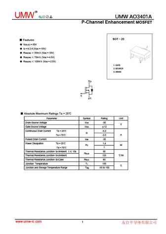
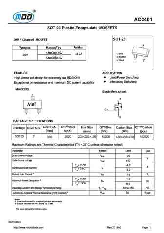
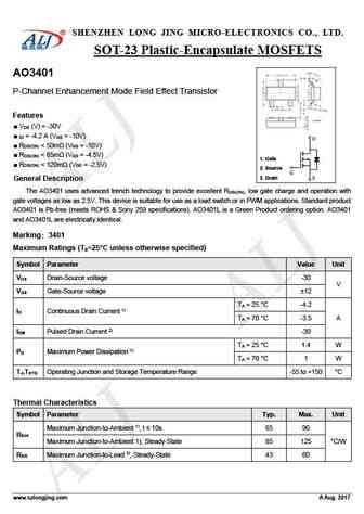
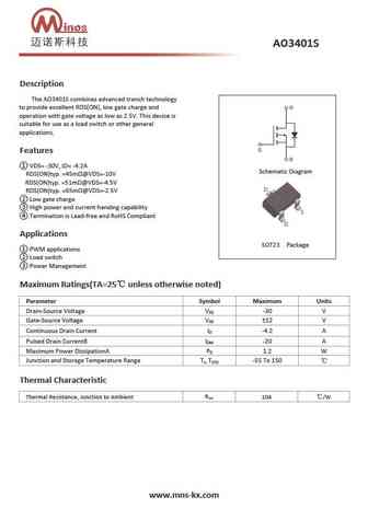
ao3401.pdf
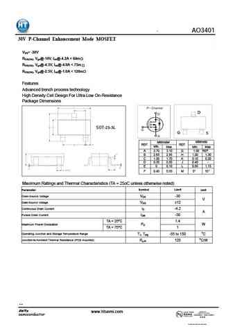
AO3401 30V P-Channel Enhancement Mode MOSFET V = -30V DS R , V DS(ON) gs@-10V, I ds@-4.2A
gm3401.pdf
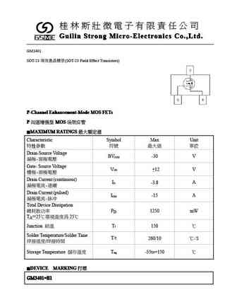
Guilin Strong Micro-Electronics Co.,Ltd. Guilin Strong Micro-Electronics Co.,Ltd. Guilin Strong Micro-Electronics Co.,Ltd. Guilin Strong Micro-Electronics Co.,Ltd. GM3401 SOT-23 (SOT-23 Field Effect Transistors) P-Channel Enhancement-Mode MOS FETs P-Channel Enhancement-Mode MOS FETs P-Channel Enhancement-Mode MOS FET
ao3401.pdf
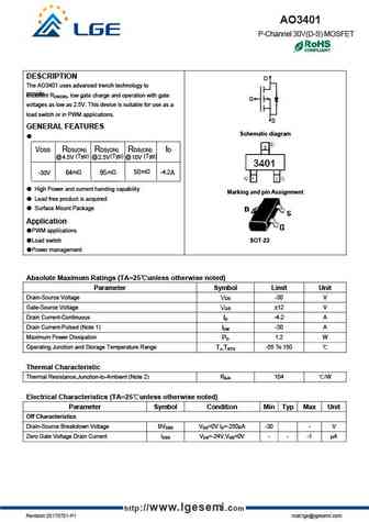
AO3401 P-Channel 30V(D-S) MOSFET DESCRIPTION D The AO3401 uses advanced trench technology to provide excellent RDS(ON), low gate charge and operation with gate G voltages as low as 2.5V. This device is suitable for use as a load switch or in PWM applications. S GENERAL FEATURES Schematic diagram VDSS RDS(ON) RDS(ON) RDS(ON) ID @ 4.5V (Typ) @ 2.5V (Typ) @ 10V (Typ)
wtc3401.pdf
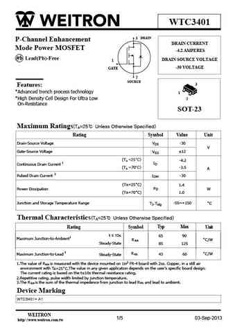
WTC3401 3 DRAIN P-Channel Enhancement DRAIN CURRENT Mode Power MOSFET -4.2 AMPERES DRAIN SOURCE VOLTAGE 1 -30 VOLTAGE GATE 2 SOURCE 3 Features *Advanced trench process technology 1 *High Density Cell Design For Ultra Low 2 On-Resistance SOT-23 Maximum Ratings(TA=25 Unless Otherwise Specified) Rating Symbol Value Unit Drain-Source Voltage -30 VDS V Gate-Source Vo
se3401.pdf
FM120-M WILLAS THRU SE340 SOT-23 Plastic-Encapsulate MOSFETS FM1200-M 1.0A SURFACE MOUNT SCHOTTKY BARRIER RECTIFIERS -20V- 200V SOD-123 PACKAGE Pb Free Produ Package outline Features Batch process design, excellent power dissipation offers better reverse leakage current and thermal resistance. SOD-123H Low profile surface mounted application in order to optimize bo
wpm3401.pdf
WPM3401 WPM3401 Single P-Channel, -30V, -4.6A, Power MOSFET www.sh-willsemi.com VDS (V) Max RDS (on) (m ) 53@ VGS=-10V -30 56@ VGS=-4.5V Descriptions SOT-23-3L The WPM3401 is the P-Channel logic enhancement D mode power field effect transistors are produced using 3 high cell density, DMOS trench technology. This high density process is especially tailored to minimiz
ao3401.pdf
AO3401 30V P-Channel MOSFET General Description Product Summary VDS -30V The AO3401 uses advanced trench technology to provide excellent RDS(ON), low gate charge and operation with gate ID (at VGS=-10V) -4.0A voltages as low as 2.5V. This device is suitable for use as RDS(ON) (at VGS=-10V)
ao3401a.pdf
AO3401A 30V P-Channel MOSFET General Description Product Summary VDS -30V The AO3401A uses advanced trench technology to provide excellent RDS(ON) , low gate charge and operation ID (at VGS=-10V) -4.0A gate voltages as low as 2.5V. This device is suitable for RDS(ON) (at VGS=-10V)
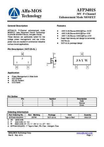
afp3401as.pdf
AFP3401AS Alfa-MOS 30V P-Channel Technology Enhancement Mode MOSFET General Description Features AFP3401AS, P-Channel enhancement mode -30V/-2.4 RDS(ON)=70 @VGS=-10.0V MOSFET, uses Advanced Trench Technology -30V/-1.8 RDS(ON)=80 @VGS=-4.5V to provide excellent RDS(ON), low gate charge. -30V/-1.2 RDS(ON)=105 @VGS=-2.5V These devices are particularly suited for lo
afp3401s.pdf
AFP3401S Alfa-MOS 30V P-Channel Technology Enhancement Mode MOSFET General Description Features AFP3401S, P-Channel enhancement mode -30V/-4.0A,RDS(ON)=65m @VGS=-10.0V MOSFET, uses Advanced Trench Technology -30V/-3.2A,RDS(ON)=80m @VGS=-4.5V to provide excellent RDS(ON), low gate charge. -30V/-1.0A,RDS(ON)=105m @VGS=-2.5V These devices are particularly suited fo
ao3401.pdf
Shenzhen Tuofeng Semiconductor Technology Co., Ltd AO3401 AO3401 P-Channel Enhancement Mode Field Effect Transistor General Description Features The AO3401 uses advanced trench technology to VDS (V) = -30V provide excellent RDS(ON), low gate charge and ID = -4.0 A (VGS = -10V) operation with gate voltages as low as 2.5V. This RDS(ON)
mtp3401n3.pdf
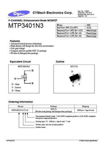
Spec. No. C388N3 Issued Date 2007.06.13 CYStech Electronics Corp. Revised Date 2017.06.19 Page No. 1/9 P-CHANNEL Enhancement Mode MOSFET BVDSS -30V MTP3401N3 ID@VGS=-10V, TA=25 C -4.2A RDS(ON)@VGS=-10V, ID=-4.2A 46m (typ) RDS(ON)@VGS=-4.5V, ID=-4A 51m (typ) RDS(ON)@VGS=-2.5V, ID=-1A 59m (typ) Features Advanced trench process technology High density c
3401l.pdf
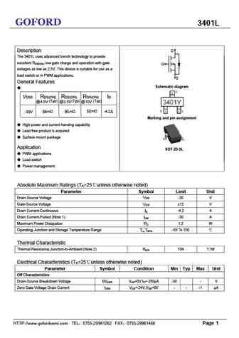
GOFORD 3401L Description D The 3401L uses advanced trench technology to provide excellent RDS(ON), low gate charge and operation with gate G voltages as low as 2.5V. This device is suitable for use as a load switch or in PWM applications. S General Features Schematic diagram VDSS RDS(ON) RDS(ON) RDS(ON) ID @ 4.5V (Typ) @ 2.5V (Typ) @ 10V (Typ) m m m 50 -4.2
sts3401a.pdf
Gre r r P Pr Pr Pro STS3401A a S mHop Microelectronics C orp. Ver 1.0 P-Channel Enhancement Mode Field Effect Transistor FEATURES PRODUCT SUMMARY Super high dense cell design for low RDS(ON). VDSS ID RDS(ON) (m ) Max Rugged and reliable. 79 @ VGS=-10V Suface Mount Package. -30V -3.2A 127 @ VGS=-4.5V D SOT-23 D G S G S (TA=25 C unless otherwise noted) ABSOLUTE MAXI
sts3401.pdf
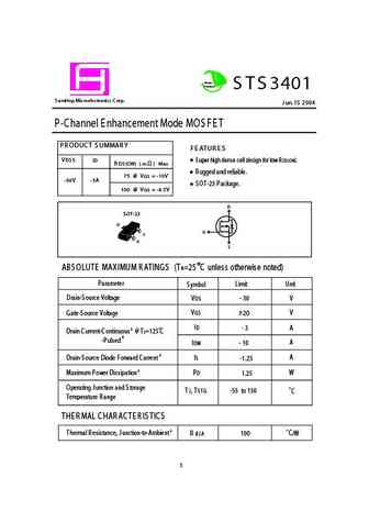
Green Product S TS 3401 S amHop Microelectronics C orp. J un.15 2004 P-Channel E nhancement Mode MOS FE T PR ODUC T S UMMAR Y F E ATUR E S VDS S ID S uper high dense cell design for low R DS (ON). R DS (ON) ( m ) Max R ugged and reliable. 75 @ VG S = -10V -30V -3A S OT-23 Package. 100 @ VG S = -4.5V D S OT-23 G S ABS OLUTE MAXIMUM R ATINGS (TA=25 C unless otherwise noted)
cs3401 sot-23-3.pdf
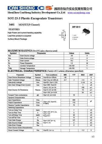
ShenZhen CanSheng Industry Development Co.,Ltd. www.szcansheng.com SOT-23-3 Plastic-Encapsulate Transistors 3401 MOSFET(P-Channel) FEATURES High Power and current handing capability Lead free product is acquired Surface Mount Package MAXIMUM RATINGS (TA=25 unless otherwise noted) Symbol Parameter Value Units VDS Drain-Source volta
ao3401.pdf
AO3401 Rev.A Aug.-2016 DATA SHEET / Descriptions SOT23-3 P MOS P- CHANNEL MOSFET in a SOT23-3 Plastic Package. / Features VDS (V) = -30V ID = -4.2 A (VGS = -10V) RDS(ON)
mmftp3401.pdf
MMFTP3401 P-Channel Enhancement Mode MOSFET 1. Gate 2. Source 3. Drain TO-236 Plastic Package Absolute Maximum Ratings Parameter Symbol Value Unit Drain-Source Voltage -VDS 30 V Gate-Source Voltage VGS 12 V Drain Current T = 25 4 A -ID A 3.2 T = 70 A Peak Drain Current 1) -IDM 27 A Power Dissipation 2) T = 25 A 1.4 PD W 0.9 T = 70 A Junction and St
lp3401lt1g.pdf
LESHAN RADIO COMPANY, LTD. 30V P-Channel Enhancement-Mode MOSFET LP3401LT1G APPLICATIONS 1)Advanced trench process technology 2)High Density Cell Design For Ultra Low On-Resistance. 3 3)We declare that the material of product compliant with RoHS requirements and Halogen Free. 1 FEATURES 2 2)RDS(ON)
sm3401nsqg.pdf
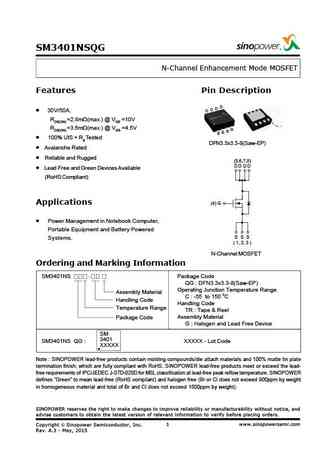
SM3401NSQG N-Channel Enhancement Mode MOSFET Features Pin Description D D D 30V/50A, D RDS(ON) =2.8m (max.) @ VGS =10V RDS(ON) =3.6m (max.) @ VGS =4.5V G S S S 100% UIS + Rg Tested DFN3.3x3.3-8(Saw-EP) Avalanche Rated Reliable and Rugged (5,6,7,8) D D DD Lead Free and Green Devices Available (RoHS Compliant) Applications (4) G Power Management in Notebook Com
wpm3401.pdf
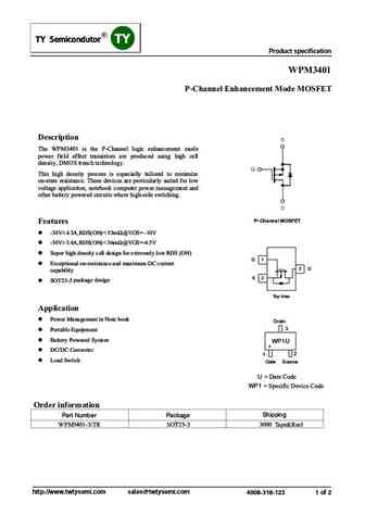
Product specification WPM3401 P-Channel Enhancement Mode MOSFET Description The WPM3401 is the P-Channel logic enhancement mode power field effect transistors are produced using high cell density, DMOS trench technology. This high density process is especially tailored to minimize on-state resistance. These devices are particularly suited for low voltage application, notebook co
dmg3401lsn.pdf
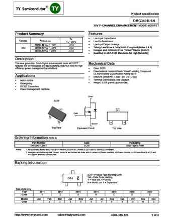
Product specification DMG3401LSN 30V P-CHANNEL ENHANCEMENT MODE MOSFET Product Summary Features Low Input Capacitance ID V(BR)DSS RDS(on) max Low On-Resistance TA = 25 C Low Input/Output Leakage 50m @ VGS = -10V -3.7A Totally Lead-Free & Fully RoHS Compliant (Notes 1 & 2) -30V 60m @ VGS = -4.5V -3.3A Halogen and Antimony Free. Green Device (
ftk3401.pdf
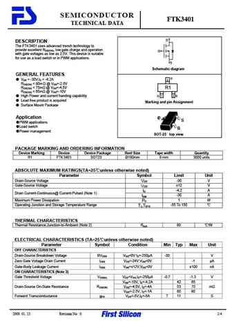
SEMICONDUCTOR FTK3401 TECHNICAL DATA D DESCRIPTION The FTK3401 uses advanced trench technology to provide excellent RDS(ON), low gate charge and operation G with gate voltages as low as 2.5V. This device is suitable for use as a load switch or in PWM applications. S Schematic diagram GENERAL FEATURES D VDS = -30V,ID = -4.2A 3 RDS(ON)
ao3401hf.pdf
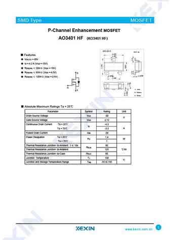
SMD Type MOSFET P-Channel Enhancement MOSFET AO3401 HF (KO3401 HF) SOT-23-3 Unit mm +0.2 2.9 -0.1 Features +0.1 0.4-0.1 VDS (V) =-30V 3 ID =-4.2 A (VGS =-10V) RDS(ON) 50m (VGS =-10V) RDS(ON) 65m (VGS =-4.5V) 1 2 D +0.02 +0.1 0.15 -0.02 0.95 -0.1 RDS(ON) 120m (VGS =-2.5V) +0.1 1.9 -0.2 G 1. Gate S 2. Source 3. Drain A
ko3401.pdf
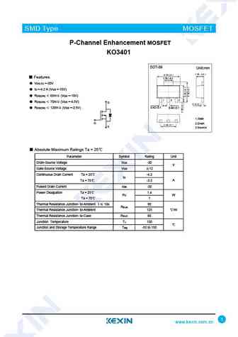
SMD Type MOSFET P-Channel Enhancement MOSFET KO3401 SOT-89 Unit mm Features 1.70 0.1 VDS (V) =-30V ID =-4.2 A (VGS =-10V) RDS(ON) 65m (VGS =-10V) RDS(ON) 70m (VGS =-4.5V) D 0.42 0.1 RDS(ON) 120m (VGS =-2.5V) 0.46 0.1 1.Gate G 2.Drain S 3.Source Absolute Maximum Ratings Ta = 25 Parameter Symbol Rating Unit Drain-Source
ao3401-3.pdf

SMD Type MOSFET P-Channel Enhancement MOSFET AO3401 (KO3401) SOT-23-3 Unit mm +0.2 2.9 -0.1 Features +0.1 0.4-0.1 VDS (V) =-30V 3 ID =-4.2 A (VGS =-10V) RDS(ON) 50m (VGS =-10V) RDS(ON) 65m (VGS =-4.5V) 1 2 D +0.02 +0.1 0.15 -0.02 0.95 -0.1 RDS(ON) 120m (VGS =-2.5V) +0.1 1.9 -0.2 G 1. Gate S 2. Source 3. Drain Absolu
ao3401 ko3401.pdf

SMD Type MOSFET P-Channel Enhancement MOSFET AO3401 (KO3401) SOT-23 Unit mm 2.9+0.1 -0.1 +0.1 0.4-0.1 Features 3 VDS (V) =-30V ID =-4.2 A (VGS =-10V) RDS(ON) 50m (VGS =-10V) 1 2 +0.1 RDS(ON) 65m (VGS =-4.5V) +0.05 0.95 -0.1 0.1 -0.01 D +0.1 1.9 -0.1 RDS(ON) 120m (VGS =-2.5V) 1. Gate G 2. Source S 3. Drain Absolute M
ao3401.pdf

SMD Type MOSFET P-Channel Enhancement MOSFET AO3401 (KO3401) SOT-23 Unit mm 2.9+0.1 -0.1 +0.1 0.4-0.1 Features 3 VDS (V) =-30V ID =-4.2 A (VGS =-10V) RDS(ON) 50m (VGS =-10V) 1 2 +0.1 RDS(ON) 65m (VGS =-4.5V) +0.05 0.95 -0.1 0.1 -0.01 D +0.1 1.9 -0.1 RDS(ON) 120m (VGS =-2.5V) 1. Gate G 2. Source S 3. Drain Absolute M
ao3401a.pdf

SMD Type MOSFET P-Channel MOSFET AO3401A (KO3401A) SOT-23 Unit mm +0.1 2.9 -0.1 +0.1 0.4 -0.1 Features 3 VDS (V) =-30V ID =-4 A (VGS =-10V) RDS(ON) 50m (VGS =-10V) 1 2 +0.1 +0.05 0.95-0.1 0.1-0.01 RDS(ON) 60m (VGS =-4.5V) +0.1 1.9-0.1 RDS(ON) 85m (VGS =-2.5V) 1. Gate 2. Source D 3. Drain G S Absolute Maximum Ratings T
ao3401a-3.pdf

SMD Type MOSFET P-Channel MOSFET AO3401A (KO3401A) SOT-23-3 Unit mm +0.2 2.9 -0.1 +0.1 0.4-0.1 3 Features VDS (V) =-30V ID =-4 A (VGS =-10V) 1 2 RDS(ON) 50m (VGS =-10V) +0.02 +0.1 0.15 -0.02 0.95 -0.1 +0.1 RDS(ON) 60m (VGS =-4.5V) 1.9 -0.2 RDS(ON) 85m (VGS =-2.5V) 1. Gate 2. Source D 3. Drain G S Absolute Maximum R
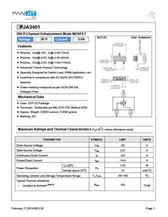
pja3401.pdf
PPJA3401 30V P-Channel Enhancement Mode MOSFET SOT-23 Unit inch(mm) Voltage -30 V Current -3.6A Features RDS(ON) , VGS@-10V, ID@-3.6A
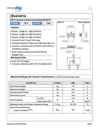
ppja3401a.pdf
PPJA3401A 30V P-Channel Enhancement Mode MOSFET SOT-23 Unit inch(mm) Voltage -30 V Current -3.6A Features RDS(ON) , VGS@-10V, ID@-3.6A
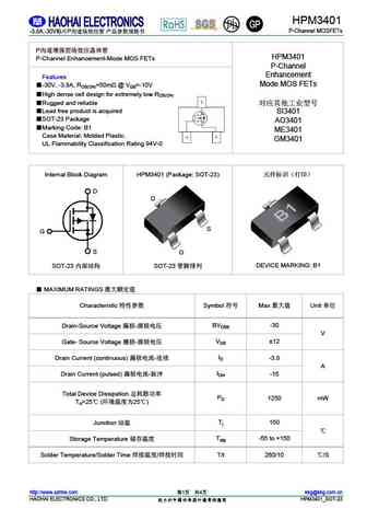
am3401.pdf
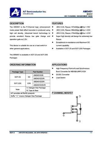
AiT Semiconductor Inc. AM3401 www.ait-ic.com MOSFET -30V P-CHANNEL ENHANCEMENT MODE DESCRIPTION FEATURES The AM3401 is the P-Channel logic enhancement -30V/-4.3A, R =47m (typ.)@V =-10V DS(ON) GS mode power field effect transistor is produced using -30V/-3.5A, R =55m (typ.)@V =-4.5V DS(ON) GS high cell density. Advanced trench technology to -30V/-2.5A, R =70m (typ.
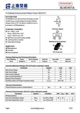
blm3401.pdf
P-Channel Enhancement BLM3401 Mode MOSFET BLM3401 BLM3401 BLM3401 FEATURES APPLICATIONS VDS VGS RDSon TYP ID Load Switch 51mR@-10V 4A Portable Devices 30V 12V 60mR@-4V5 DCDC conversion 98mR@-2V5 Pin Configuration DESCRIPTION This device is particularly suited for low voltage application such as portable equipment, power management and other
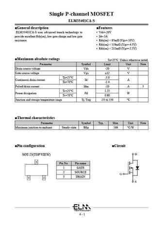
elm53401ca.pdf
Single P-channel MOSFET ELM53401CA-S General description Features ELM53401CA-S uses advanced trench technology to Vds=-20V provide excellent Rds(on), low gate charge and low gate Id=-1.8A resistance. Rds(on)
elm33401ca-s.pdf
Single P-channel MOSFET ELM33401CA-S General description Features ELM33401CA-S uses advanced trench technology to Vds=-20V provide excellent Rds(on), low gate charge and low gate Id=-3A resistance. Rds(on)
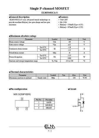
elm13401ca.pdf
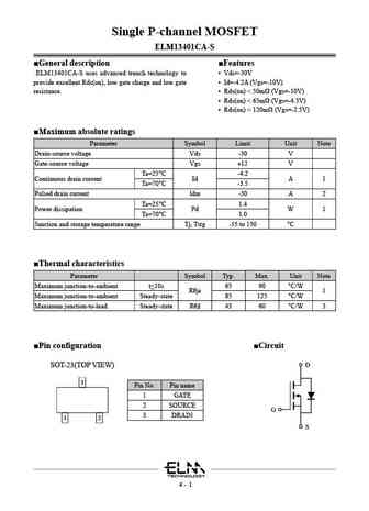
Single P-channel MOSFET ELM13401CA-S General description Features ELM13401CA-S uses advanced trench technology to Vds=-30V provide excellent Rds(on), low gate charge and low gate Id=-4.2A (Vgs=-10V) resistance. Rds(on)
gsm3401s.pdf
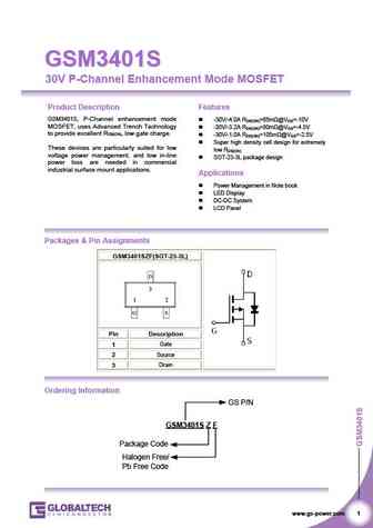
GSM3401S GSM3401S 30V P-Channel Enhancement Mode MOSFET Product Description Features GSM3401S, P-Channel enhancement mode -30V/-4.0A RDS(ON)=65m @VGS=-10V MOSFET, uses Advanced Trench Technology -30V/-3.2A RDS(ON)=80m @VGS=-4.5V to provide excellent RDS(ON), low gate charge. -30V/-1.0A RDS(ON)=105m @VGS=-2.5V Super high density cell design for extremely These devi
gsm3401as.pdf
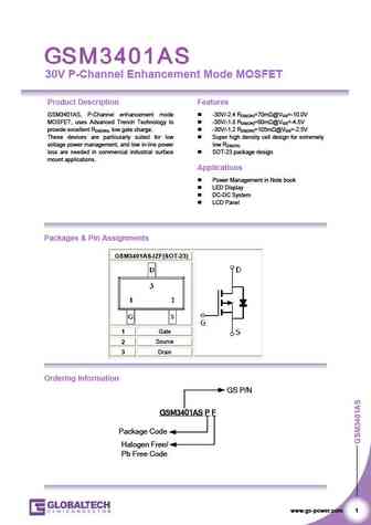
30V P-Channel Enhancement Mode MOSFET Product Description Features GSM3401AS, P-Channel enhancement mode -30V/-2.4 RDS(ON)=70m @VGS=-10.0V MOSFET, uses Advanced Trench Technology to -30V/-1.8 RDS(ON)=80m @VGS=-4.5V provide excellent RDS(ON), low gate charge. -30V/-1.2 RDS(ON)=105m @VGS=-2.5V These devices are particularly suited for low Super high density cell de
kia3401.pdf
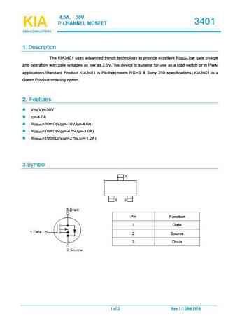
-4.0A -30V 3401 P-CHANNELMOSFET KIA KIA KIA SEMICONDUCTORS SEMICONDUCTORS SEMICONDUCTORS 1.Description The KIA3401 uses advanced trench technology to provide excellent R ,lowgate charge DS(on) and operation with gate voltages as lowas 2.5V.This device is suitable for use as a load switch or in PWM applications.Standard Product KIA3401 is Pb-free(meets ROHS & Sony 259 specificatio
mmp3401.pdf
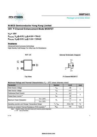
MMP3401 Package Level Data Sheet M-MOS Semiconductor Hong Kong Limited 30V P-Channel Enhancement-Mode MOSFET VDS= -30V RDS(ON), Vgs@-4.5V, Ids@-4.0A = 75m RDS(ON), Vgs@-2.5V, Ids@-1.0A = 120m Features Advanced trench process technology High Density Cell Design For Ultra Low On-Resistance SOT -23 Internal Schematic Diagram Top View P-Channel MOSFET Maximum Ratings and Thermal C
nce3401a.pdf
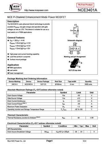
Pb Free Product http //www.ncepower.com NCE3401A NCE P-Channel Enhancement Mode Power MOSFET Description The NCE3401A uses advanced trench technology to provide D excellent RDS(ON), low gate charge and operation with gate voltages as low as 2.5V. This device is suitable for use as a G load switch or in PWM applications. S General Features VDS = -30V,ID = -4.4A Schematic
nce3401.pdf
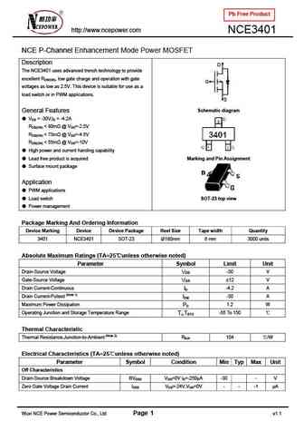
Pb Free Product http //www.ncepower.com NCE3401 NCE P-Channel Enhancement Mode Power MOSFET Description D The NCE3401 uses advanced trench technology to provide excellent RDS(ON), low gate charge and operation with gate G voltages as low as 2.5V. This device is suitable for use as a load switch or in PWM applications. S Schematic diagram General Features VDS = -30V,ID
nce3401by.pdf
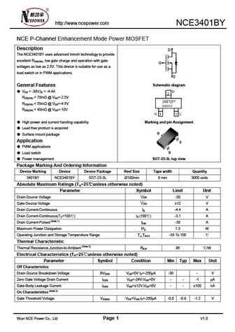
http //www.ncepower.com NCE3401BY NCE P-Channel Enhancement Mode Power MOSFET Description D The NCE3401BY uses advanced trench technology to provide excellent RDS(ON), low gate charge and operation with gate G voltages as low as 2.5V. This device is suitable for use as a load switch or in PWM applications. S Schematic diagram General Features VDS = -30V,ID = -4.4A RD
nce3401y.pdf
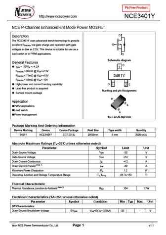
Pb Free Product http //www.ncepower.com NCE3401Y NCE P-Channel Enhancement Mode Power MOSFET D Description The NCE3401Y uses advanced trench technology to provide G excellent RDS(ON), low gate charge and operation with gate voltages as low as 2.5V. This device is suitable for use as a load switch or in PWM applications. S Schematic diagram General Features VDS = -30V,
nce3401ay.pdf
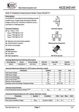
http //www.ncepower.com NCE3401AY NCE P-Channel Enhancement Mode Power MOSFET Description D The NCE3401AY uses advanced trench technology to provide excellent RDS(ON), low gate charge and operation with gate G voltages as low as 2.5V. This device is suitable for use as a load switch or in PWM applications. S Schematic diagram General Features VDS = -30V,ID = -4.4A RD
nce3401e.pdf
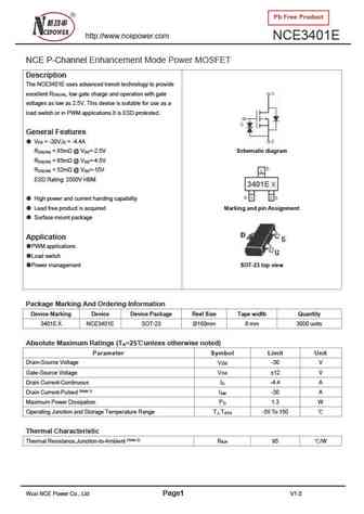
Pb Free Product http //www.ncepower.com NCE3401E NCE P-Channel Enhancement Mode Power MOSFET Description The NCE3401E uses advanced trench technology to provide excellent R , low gate charge and operation with gate DS(ON) voltages as low as 2.5V. This device is suitable for use as a load switch or in PWM applications.It is ESD protested. General Features V = -30V,I = -4.4A DS D
smc3401.pdf
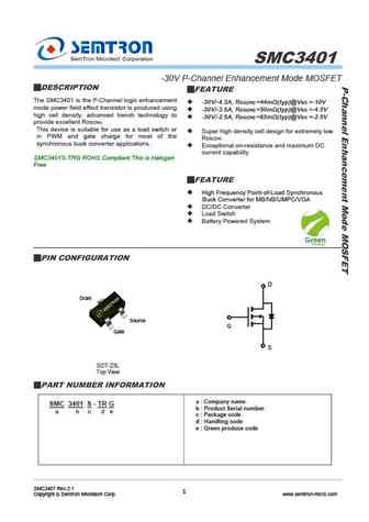
SMC3401 -30V P-Channel Enhancement Mode MOSFET DESCRIPTION FEATURE The SMC3401 is the P-Channel logic enhancement -30V/-4.3A, RDS(ON) =44m (typ)@VGS =-10V mode power field effect transistor is produced using -30V/-3.5A, RDS(ON) =50m (typ)@VGS =-4.5V high cell density. advanced trench technology to -30V/-2.5A, RDS(ON) =65m (typ)@VGS =-2.5V provide excelle
stp3401a.pdf
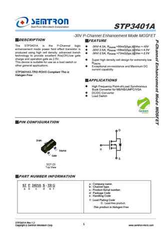
STP3401A -30V P-Channel Enhancement Mode MOSFET DESCRIPTION FEATURE The STP3401A is the P-Channel logic -30V/-4.3A, RDS(ON) =50m (typ.)@VGS =-10V enhancement mode power field effect transistor is -30V/-3.5A, RDS(ON) =58m (typ.)@VGS =-4.5V produced using high cell density. advanced trench -30V/-2.5A, RDS(ON) =73m (typ.)@VGS =-2.5V technology to provide exc
stp3401.pdf
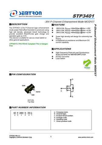
STP3401 -30V P-Channel Enhancement Mode MOSFET DESCRIPTION FEATURE The STP3401 is the P-Channel logic enhancement -30V/-4.3A, RDS(ON) =44m (typ.)@VGS =-10V mode power field effect transistor is produced using -30V/-3.5A, RDS(ON) =50m (typ.)@VGS =-4.5V high cell density. advanced trench technology to -30V/-2.5A, RDS(ON) =65m (typ.)@VGS =-2.5V provide exce
sl3401a.pdf
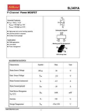
SL3401A SOT-23 Package Information Dimensions in Millimeters Symbol MIN. MAX. A 0.900 1.150 A1 0.000 0.100 A2 0.900 1.050 b 0.300 0.500 c 0.080 0.150 D 2.800 3.000 E 1.200 1.400 E1 2.250 2.550 e 0.950TYP e1 1.800 2.000 L 0.550REF L1 0.300 0.500 0 8 www.slkormicro.com 4
sl3401.pdf
SL3401 P-Channel Power MOSFET D General Features G VDS = -30V,ID = -4.1A RDS(ON)
sl3401s.pdf
SL3401S P-Channel Power MOSFET D General Features G VDS = -30V,ID = -4A RDS(ON)
st3401m23rg.pdf
ST3401M23RG P Channel Enhancement Mode MOSFET -4.0A DESCRIPTION ST3401M23RG is the P-Channel logic enhancement mode power field effect transistor which is produced using high cell density DMOS trench technology. This high density process is especially tailored to minimize on-state resistance. These devices are particularly suited for low voltage application such as cellular phon
st3401srg.pdf
ST3401SRG P Channel Enhancement Mode MOSFET -4.0A DESCRIPTION ST3401RSG is the P-Channel logic enhancement mode power field effect transistor which is produced using high cell density DMOS trench technology. This high density process is especially tailored to minimize on-state resistance. These devices are particularly suited for low voltage application such as cellular phone an
ao3401a.pdf
R UMWpe UMW AO3401A UMW AO3401A M SFET SMD Ty P-Channel Enhancement MOSFET SOT 23 Features VDS (V) =-30V ID =-4.2 A (VGS =-10V) RDS(ON) 55m (VGS =-10V) RDS(ON) 70m (VGS =-4.5V) RDS(ON) 120m (VGS =-2.5V) 1. GATE 2. SOURCE 3. DRAIN D G S Absolute Maximum Ratings Ta = 25 Parameter Symbol Rating Unit Drain-Source Voltage V
atm3401psa.pdf
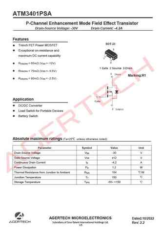
ATM3401PSA P-Channel Enhancement Mode Field Effect Transistor Drain-Source Voltage -30V Drain Current -4.2A Features Trench FET Power MOSFET Exceptional on-resistance and maximum DC current capability R
atm3401apsa.pdf
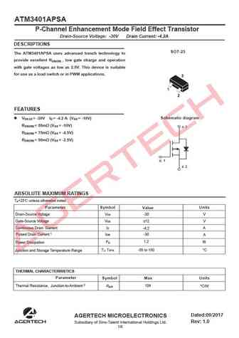
ATM3401APSA P-Channel Enhancement Mode Field Effect Transistor Drain-Source Voltage -30V Drain Current -4.2A DESCRIPTIONS SOT-23 The ATM3401APSA uses advanced trench technology to provide excellent RDS(ON) , low gate charge and operation with gate voltages as low as 2.5V. This device is suitable for use as a load switch or in PWM applications. FEATURES Schematic diagram V =
as3401.pdf
P-Channel MOSFET AS3401 SOT-23 Plastic-Encapsulate MOSFETS SOT-23 FEATURE TrenchFET Power MOSFET 1. GATE APPLICATIONS 2. SOURCE Load Switch for Portable Devices 3. DRAIN DC/DC Converter MARKING X 1 or B 1 Maximum ratings (Ta=25 unless otherwise noted) Characteristic Symbol Max Unit Drain-Source Voltage BV -30 V DSS
asdm3401zb.pdf
ASDM3401ZB -30V P-CHANNEL MOSFET FEATURES Product Summary High dense cell design for extremely low RDS(ON). Exceptional on-resistance and maximum DC current capability V DS -30 V R DS(on),Max@ VGS=-10 V 65 m Application I D -4.2 A PWM applications Load switch Power management top view D G S SOT-23 Maximum ratings ( Ta=25 unless otherwise noted)
ao3401a.pdf
AO3401A MOSFET ROHS P-Channel Enhancement-Mode MOSFET SOT-23 - Features Advanced trench process technology High Density Cell Design For Ultra Low On-Resistance MAXIMUM RANTINGS Characteristic Symbol Max Unit -30 Drain-Source Voltage BV V DSS Gate- Source Voltage V V GS +12 Drain Current (continuous) I -4.2 A D Drain Current (pulsed) I A DM -18 Total Device D
ev3401.pdf
Eternal Semiconductor Inc. EV3401 P-Channel Enhancement-Mode MOSFET (-30V, -4.2A) PRODUCT SUMMARY VDSS ID RDS(on) (m ) Typ. 53 @ VGS = -10 V,ID=-4.2A -30V -4.2A 64 @ VGS = -4.5V,ID=-4.0A 86 @ VGS = -2.5V,ID=-1.0A Features Super high dense cell trench design for low RDS(on) Rugged and reliable SOT-23-3L package Lead Pb -free and halogen-free EV3401 Pin Assignm
gp3401.pdf
GP3401 30V P-Channel MOSFET Product Summary SOT-23 V R I (BR)DSS DS(on)MAX D 65m @-10V D -30V 75m @-4.5V -4.2A 90m @-2.5V G Feature S TrenchFET Power MOSFET Schematic diagram Exceptional on-resistance and maximum DC current capability Application D DC/DC Converter Load Switch for Portable Devices Battery Switch G MARKING S ABSOLUTE
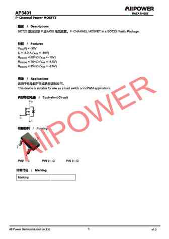
ao3401.pdf
Plastic-Encapsulate Mosfets AO3401 P-Channel MOSFET FEATURES High dense cell design for extremely low RDS(ON). Exceptional on-resistance and maximum DC current capability D 1.Gate 2.Source SOT-23 3.Drain G S MARKING A19T Maximum ratings ( Ta=25 unless otherwise noted) Unit Parameter Symbol Value Drain-Source Voltage VDS -30 V Gate-Source Voltage VGS 12 V Continuous
hss3401a.pdf

HSS3401A P-Ch 30V Fast Switching MOSFETs Description Product Summary V -30 V DS The HSS3401A is the high cell density trenched P- ch MOSFETs, which provides excellent RDSON R 53 m DS(ON),max and efficiency for most of the small power switching and load switch applications. I -4.3 A D The HSS3401A meet the RoHS and Green Product requirement with full function reliabili
ao3401a.pdf

AO3401A P-Ch 30V Fast Switching MOSFETs Description Product Summary VDS -30 V The AO3401A is the high cell density trenched P- ch MOSFETs, which provides excellent RDSON RDS(ON),typ 54 m and efficiency for most of the small power switching and load switch applications. ID -4.2 A The AO3401A meet the RoHS and Green Product requirement with full function reliability approv
hx3401.pdf
SOT-23-3 Plastic-Encapsulate Transistors HX3401MOSFET(P-Channel) FEATURES High Power and current handing capability Lead free product is acquired Surface Mount Package MARKING X18V MAXIMUM RATINGS (TA=25 unless otherwise noted) Symbol Parameter Value Units VDS Drain-Source voltage -30 V VGS Gate-Source voltage 12 V ID Drain current -4.2 A PD Power Dissipation 1.2
hx3401a.pdf
SOT-23-3Plastic-Encapsulate Transistors HX3401A MOSFET(P-Channel) FEATURES TrenchFET Power MOSFET MARKING A19T MAXIMUM RATINGS (TA=25 unless otherwise noted) Symbol Parameter Value Units VDS Drain-Source voltage -20 V VGS Gate-Source voltage 12 V -3 A ID Drain current PD Power Dissipation 1 W Tj Junction Temperature 150 Tstg Storage Temperature -55-150 ELECTRICAL CHA
jmtj3401a.pdf
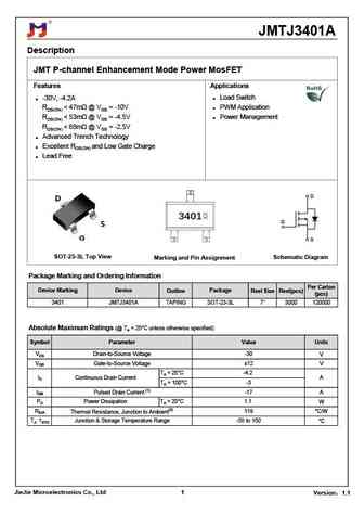
JMTJ3401A Description JMT P-channel Enhancement Mode Power MosFET Features Applications -30V, -4.2A Load Switch RDS(ON)
jmtl3401b.pdf
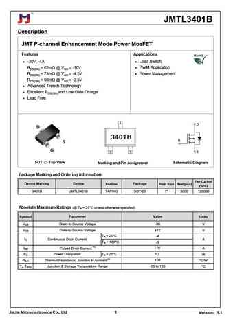
JMTL3401B Description JMT P-channel Enhancement Mode Power MosFET Features Applications -30V, -4A Load Switch RDS(ON)
jmtl3401a.pdf
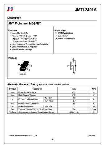
JMTL3401A Description JMT P-channel Enhancement Mode Power MosFET Features Applications -30V, -4.2A Load Switch RDS(ON)
jmtj3401b.pdf

JMTJ3401B Description JMT P-channel Enhancement Mode Power MosFET Features Applications -30V, -4A Load Switch RDS(ON)
se3401.pdf
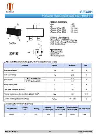
SE3401 P-Channel Enhancement Mode Power MOSFET Product Summary V -30V DS I -4.4A D R ( at V =-10V) 55 mohm DS(ON) GS R ( at V =-4.5V) 68 mohm DS(ON) GS R ( at V =-2.5V) 96 mohm DS(ON) GS General Description Trench Power LV MOSFET technology High density cell design for Low R DS(ON) High Speed switching Applications Batt
jst3401.pdf
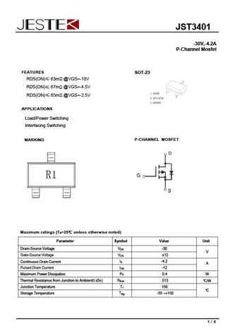
JST3401 -30V,-4.2A P-Channel Mosfet FEATURES SOT-23 RDS(ON) 63m @VGS=-10V RDS(ON) 67m @VGS=-4.5V RDS(ON) 85m @VGS=-2.5V APPLICATIONS Load/Power Switching Interfacing Switching P-CHANNEL MOSFET MARKING Maximum ratings (Ta=25 unless otherwise noted) Parameter Symbol Value Unit Drain-Source Voltage VDS -30 V Gate-Source Voltage V 12 GS I -4.2 D Continuou
jsm3401l.pdf
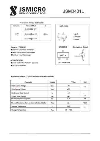
JSM3401L P-Channel 30-V(D-S) MOSFET V(BR)DSS RDS(on)MAX ID SOT-23-3L 0.053 @-10V 3 -30V 0.065 @-4.5V 1.GATE -4.2A 2.SOURCE 0.085 @-2.5V 3.DRAIN 1 2 MARKING Equivalent Circuit General FEATURE TrenchFET Power MOSFET Lead free product is acquired Surface mount package A19TF w APPLICATION *w week code Load Switch for Portable Devices DC/DC Converter Maximu
lpm3401.pdf
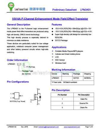
Preliminary Datasheet LPM3401 15V/4A P-Channel Enhancement Mode Field Effect Transistor General Description Features The LPM3401 is the P-channel logic enhancement -15V/-4.0A,RDS(ON) 58m (typ.)@VGS=-10V mode power field effect transistors are produced using -15V/-3.0A,RDS(ON) 68m (typ.)@VGS=-4.5V high cell density, DMOS trench technology. Super high density cell desi
ao3401.pdf
AO3401 SOT-23 Plastic-Encapsulate MOSFETS SOT-23 30V P-Channel MOSFET 3 ID Max V(BR)DSS RDS(on)Typ 44m @-10V 1. GATE -4.2A -30V 2. SOURCE 51m @4.5V 1 3. DRAIN 2 FEATURE APPLICATION Load/Power Switching High dense cell design for extremely low RDS(ON) Interfacing Switching Exceptional on-resistance and maximum DC current capability MARKING Equivalen
ao3401mi-ms.pdf
www.msksemi.com AO3401MI-MS Semiconductor Compiance FEATURE SOT-23-3 3 High dense cell design for extremely low R . DS(ON) Exceptional on-resistance and maximum DC currentcapability 1. GATE 1 2 APPLICATION 2. SOURCE Load/Power Switching 3. DRAIN Interfacing Switching Equivalent Circuit I V(BR)DSS RDS(on)MAX D 65m @-10V 75m @-4.5V -30 V -4.2A 90m @-2.5V
si3401.pdf
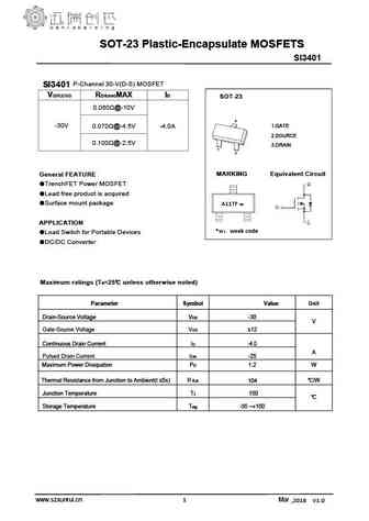
SOT-23 Plastic-Encapsulate MOSFETS SI3401 P-Channel 30-V(D-S) MOSFET SI3401 V(BR)DSS RDS(on)MAX ID SOT-23 0.060 @-10V 3 -30V 0.070 @-4.5V 1.GATE -4.0A 2.SOURCE 0.100 @-2.5V 3.DRAIN 1 2 MARKING Equivalent Circuit General FEATURE TrenchFET Power MOSFET Lead free product is acquired Surface mount package A11TF w APPLICATION *w week code Load Switch for Porta
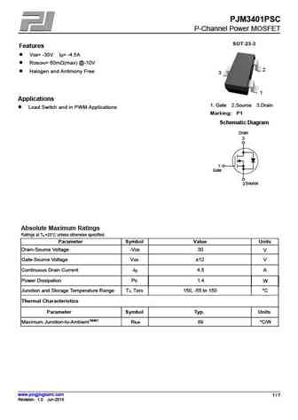
pjm3401psc.pdf
PJM3401PSC P-Channel Power MOSFET SOT-23-3 Features VDS= -30V I = -4.5A D RDS(ON)= 60m (max) @-10V 2 Halogen and Antimony Free 3 1 Applications 1. Gate 2.Source 3.Drain Load Switch and in PWM Applications Marking P1 Schematic Diagram Drain 3 1 Gate Source 2 Absolute Maximum Ratings Ratings at TA =25 unless otherwise specified. Parameter Symbol Valu
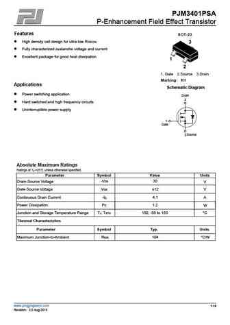
pjm3401psa.pdf
PJM3401PSA P-Enhancement Field Effect Transistor Features SOT-23 High density cell design for ultra low RDS(ON) Fully characterized avalanche voltage and current Excellent package for good heat dissipation 1. Gate 2.Source 3.Drain Marking R1 Applications Schematic Diagram Power switching application Drain 3 Hard switched and high frequency circuits Unint
sr3401.pdf
Leading Circuit Protection Products and Solutions SR3401 30V P-Channel MOSFET Product Summary SOT-23 V(BR)DSS RDS(on)MAX ID 65m @-10V D -30V 75m @-4.5V -4.2A 90m @-2.5V G Feature S TrenchFET Power MOSFET Schematic diagram Exceptional on-resistance and maximum DC current capability Application D DC/DC Converter Load Switch for Portable Devices Battery S
ao3401.pdf
AO3401 -30V P-Channel Enhancement Mode MOSFET V = -30V DS R , V DS(ON) gs@-10V, I ds@-4.2A
agm3401e.pdf
AGM3401E General Description Product Summary The AGM3401E combines advanced trench MOSFET technology with a low resistance package to provide extremely low R . DS(ON) This device is ideal for load switch and battery BVDSS RDSON ID protection applications. -30V 43.5m -4.4A Features SOT23-3 Pin Configuration Advance high cell density Trench technology Low R to m
ao3401.pdf
P-Channel Enhancement Mode MOSFET Channel Enhancement Mode MOSFET Feature SC-59 -30V/-4.2A, RDS(ON) =55m (MAX) @VGS = -10V. = RDS(ON) = 70m (MAX) @VGS = -4.5V. GS RDS(ON) =120m (MAX) @VGS = -2.5V. GS Super High dense cell design for extremely low R Super High dense cell design for extremely low RDS(ON) Reliable and Rugged SC-59 for Surface Mount Package Applications
wtm3401.pdf
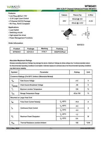
WTM3401 -30V/-4.2A P Channel Advanced Power MOSFET Features V R Typ I Max (BR)DSS DS(ON) D Low RDS(on) @VGS=-10V -3.3V Logic Level Control 55m @-10V P Channel SOT23 Package -30V -4.2A 65m @ -4.5V Pb-Free, RoHS Compliant Applications Load Switch Switching circuits High-speed line driver Power Management Functions Order Information
ao3401.pdf
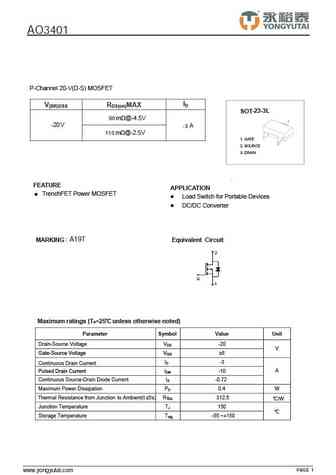
AO3401 P-Channel 20-V(D-S) MOSFET ID V(BR)DSS RDS(on)MAX SOT-23-3L 90 m @-4.5V -20V A -3 110 m @-2.5V 1. GATE 2. SOURCE 3. DRAIN FEATURE APPLICATION TrenchFET Power MOSFET z z Load Switch for Portable Devices z DC/DC Converter MARKING A19T Equivalent Circuit Maximum ratings (Ta=25 unless otherwise noted) Parameter Symbol Value Unit Drain-Source V
ao3401.pdf
SHENZHEN LONG JING MICRO-ELECTRONICS CO., LTD. SOT-23 Plastic-Encapsulate MOSFETS AO3401 P-Channel Enhancement Mode Field Effect Transistor Features V (V) = -30V DS = -4.2 A (V = -10V) ID GS R
tf3401.pdf
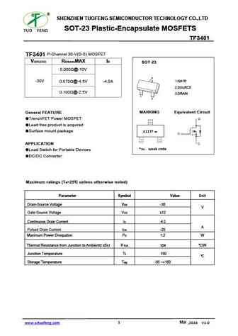
SHENZHEN TUOFENG SEMICONDUCTOR TECHNOLOGY CO.,LTD SOT-23 Plastic-Encapsulate MOSFETS TF3401 P-Channel 30-V(D-S) MOSFET TF3401 V(BR)DSS RDS(on)MAX ID SOT-23 0.060 @-10V 3 -30V 0.070 @-4.5V 1.GATE -4.0A 2.SOURCE 0.100 @-2.5V 3.DRAIN 1 2 MARKING Equivalent Circuit General FEATURE TrenchFET Power MOSFET Lead free product is acquired Surface mount package A11TF w AP
ao3401.pdf
SI2305 AO3401 AO3401 AO3401 SOT-23 Plastic-Encapsulate MOSFETS FEATURES
wst3401.pdf
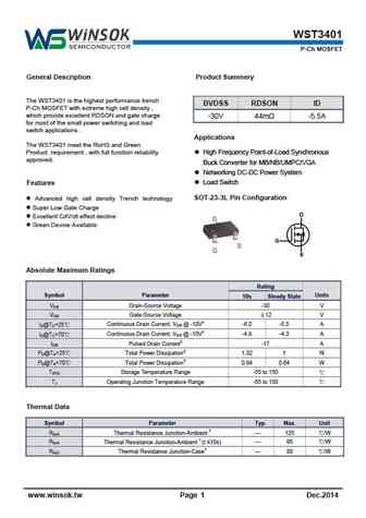
WST3401 P-Ch MOSFET General Description Product Summery The WST3401 is the highest performance trench BVDSS RDSON ID P-Ch MOSFET with extreme high cell density , which provide excellent RDSON and gate charge -30V 44m -5.5A for most of the small power switching and load switch applications . Applications The WST3401 meet the RoHS and Green Product requirement , with full
wst3401a.pdf
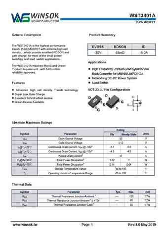
WST3401A P-Ch MOSFET General Description Product Summery The WST3401A is the highest performance BVDSS RDSON ID trench P-Ch MOSFET with extreme high cell density , which provide excellent RDSON and -30V 48m -5.0A gate charge for most of the small power switching and load switch applications . Applications The WST3401A meet the RoHS and Green Product requirement , with fu
se3401.pdf
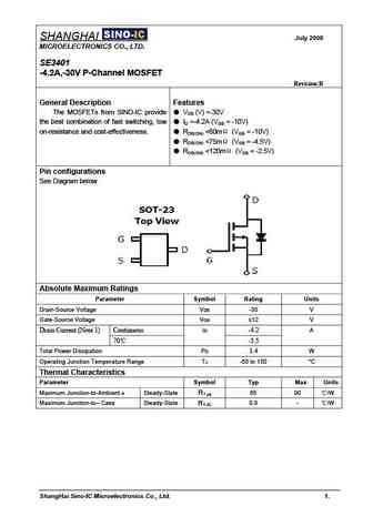
SHANGHAI July 2008 MICROELECTRONICS CO., LTD. SE3401 -4.2A,-30V P-Channel MOSFET Revision B General Description Features The MOSFETs from SINO-IC provide VDS (V) =-30V the best combination of fast switching, low ID =-4.2A (VGS = -10V) on-resistance and cost-effectiveness. RDS(ON)
se3401b.pdf
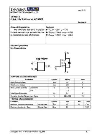
SHANGHAI Jan 2015 MICROELECTRONICS CO., LTD. SE3401B -2.8A,-20V P-Channel MOSFET Revision A General Description Features ID =-2.8A The MOSFETs from SINO-IC provide VDS (V) =-20V the best combination of fast switching, low RDS(ON)
sm3401.pdf
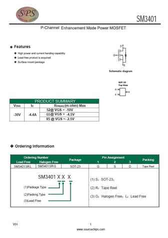
SM3401 Features Schematic diagram SOT-23 Top View G D S PRODUCT SUMMARY VDSS ID RDS(on) (m-ohm) Max 52@ VGS = -10V 65@ VGS = -4.5V -30V -4.4A 85 @ VGS =- 2.5V Ordering Information Ordering Number Pin Assignment Package Packing Lead Free Halogen Free 1 2 3 SM3401SR G SM3401SR L SOT-23 G S D Tape Reel SM3401 X X X (1) S SOT-23 (1)Packa
ao3401.pdf
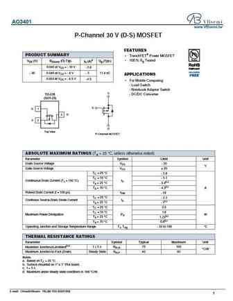
AO3401 www.VBsemi.tw P-Channel 30 V (D-S) MOSFET FEATURES PRODUCT SUMMARY TrenchFET Power MOSFET 100 % Rg Tested VDS (V) RDS(on) ( ) Typ. ID (A)a Qg (Typ.) 0.046 at VGS = - 10 V - 5.6 0.049 at VGS = - 6 V - 5 11.4 nC - 30 APPLICATIONS 0.054 at VGS = - 4.5 V -4.5 For Mobile Computing - Load Switch - Notebook Adaptor Switch S TO-236 - DC/DC Converter (SOT-23)
ao3401a.pdf

AO3401A www.VBsemi.tw P-Channel 30 V (D-S) MOSFET FEATURES PRODUCT SUMMARY TrenchFET Power MOSFET 100 % Rg Tested VDS (V) RDS(on) ( ) Typ. ID (A)a Qg (Typ.) 0.046 at VGS = - 10 V - 5.6 0.049 at VGS = - 6 V - 5 11.4 nC - 30 APPLICATIONS 0.054 at VGS = - 4.5 V -4.5 For Mobile Computing - Load Switch - Notebook Adaptor Switch S TO-236 - DC/DC Converter (SOT-23)
ge3401.pdf

GE3401 www.VBsemi.tw P-Channel 30 V (D-S) MOSFET FEATURES PRODUCT SUMMARY TrenchFET Power MOSFET 100 % Rg Tested VDS (V) RDS(on) ( ) Typ. ID (A)a Qg (Typ.) 0.046 at VGS = - 10 V - 5.6 0.049 at VGS = - 6 V - 5 11.4 nC - 30 APPLICATIONS 0.054 at VGS = - 4.5 V -4.5 For Mobile Computing - Load Switch - Notebook Adaptor Switch S TO-236 - DC/DC Converter (SOT-23)
am3401e3vr.pdf
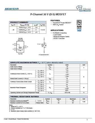
AM3401E3VR www.VBsemi.tw P-Channel 30 V (D-S) MOSFET FEATURES PRODUCT SUMMARY TrenchFET Power MOSFET 100 % Rg Tested VDS (V) RDS(on) ( ) Typ. ID (A)a Qg (Typ.) 0.046 at VGS = - 10 V - 5.6 0.049 at VGS = - 6 V - 5 11.4 nC - 30 APPLICATIONS 0.054 at VGS = - 4.5 V -4.5 For Mobile Computing - Load Switch - Notebook Adaptor Switch S TO-236 - DC/DC Converter (SOT-
yjl3401a.pdf
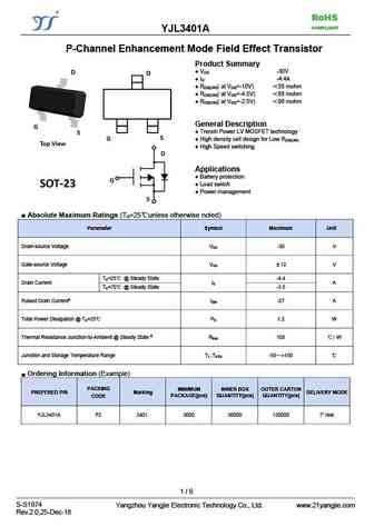
RoHS COMPLIANT YJL3401A P-Channel Enhancement Mode Field Effect Transistor Product Summary V -30V DS I -4.4A D R ( at V =-10V) 55 mohm DS(ON) GS R ( at V =-4.5V) 68 mohm DS(ON) GS R ( at V =-2.5V) 96 mohm DS(ON) GS General Description Trench Power LV MOSFET technology High density cell design for Low R DS(ON) High Speed s
ttx3401a.pdf
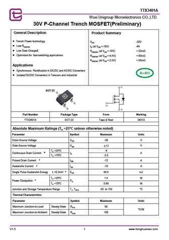
TTX3401A Wuxi Unigroup Microelectronics CO.,LTD. 30V P-Channel Trench MOSFET(Preliminary) General Description Product Summary Trench Power technology VDS -30V Low RDS(ON) ID (at VGS =-10V) -4A Low Gate Charge& RDS(ON) (at VGS =-10V)
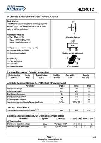
hm3401.pdf
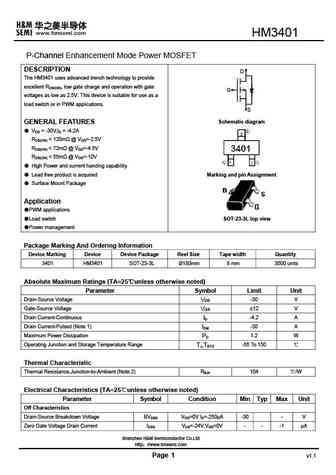
HM3401 P-Channel Enhancement Mode Power MOSFET DESCRIPTION D The HM3401 uses advanced trench technology to provide excellent RDS(ON), low gate charge and operation with gate G voltages as low as 2.5V. This device is suitable for use as a load switch or in PWM applications. S Schematic diagram GENERAL FEATURES VDS = -30V,ID = -4.2A RDS(ON)
hm3401d.pdf
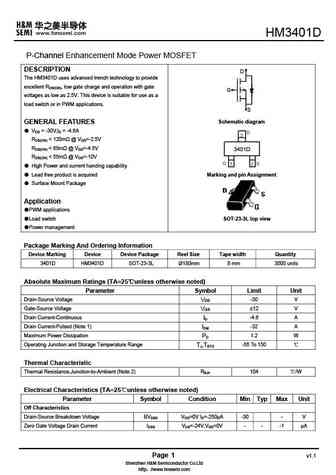
HM3401 P-Channel Enhancement Mode Power MOSFET DESCRIPTION D The HM3401 uses advanced trench technology to provide excellent RDS(ON), low gate charge and operation with gate G voltages as low as 2.5V. This device is suitable for use as a load switch or in PWM applications. S Schematic diagram GENERAL FEATURES VDS = -30V,ID = -4.6A RDS(ON)
hm3401c.pdf
HM3401C P-Channel Enhancement Mode Power MOSFET Description D The HM3401C uses advanced trench technology to provide excellent RDS(ON), This device is suitable for use as a load G switch or in PWM applications. S General Features VDS = -30V,ID = -2.5A Schematic diagram RDS(ON)
hm3401b.pdf

HM3401B P-Channel Enhancement Mode Power MOSFET DESCRIPTION D The HM3401B uses advanced trench technology to provide excellent RDS(ON), low gate charge and operation with gate G voltages as low as 2.5V. This device is suitable for use as a load switch or in PWM applications. S Schematic diagram GENERAL FEATURES VDS = -30V,ID = -4.2A RDS(ON)
hm3401pr.pdf
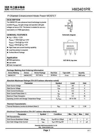
HM3401PR P-Channel Enhancement Mode Power MOSFET DESCRIPTION D The HM3401PR uses advanced trench technology to provide excellent RDS(ON), low gate charge and operation with gate G voltages as low as 2.5V. This device is suitable for use as a load switch or in PWM applications. S Schematic diagram GENERAL FEATURES VDS = -30V,ID = -5.2A RDS(ON)
ao3401s.pdf
Description The AO3401S combines advanced trench technology to provide excellent RDS(ON), low gate charge and operation with gate voltage as low as 2.5V. This device is suitable for use as a load switch or other general applications. Features VDS= -30V, ID= -4.2A Schematic Diagram RDS(ON)typ. =45m @VDS=-10V RDS(ON)typ. =51m @VDS=-4.5V RDS(ON)typ. =65m @VDS=-2.5V Low gate
hpm3401.pdf
HPM3401 P-Channel MOSFETs -3.8A,-30V P P HPM3401 P-Channel Enhancement-Mode MOS FETs P-Channel Enhancement Features Mode MOS FETs -30V, -3.8A, RDS(ON)=50m @ VGS=-10V High dense cell design for extremely low RDS(ON) Rugged and reliable Lead f
hpm3401a.pdf
HPM3401A P-Channel MOSFETs -4.2A,-30V P P HPM3401A P-Channel Enhancement-Mode MOS FETs P-Channel Enhancement Features Mode MOS FETs -30V, -4.2A, RDS(ON)=53m @ VGS=-4.5V High dense cell design for extremely low RDS(ON) Rugged and reliable Le
pm3401.pdf
PM3401 30V P-Channel MOSFET Description Applications The PM3401 uses advanced Trench technology and DC/DC Converter designs to provide excellent R with low gate charge. Load Switch for Portable Devices DS(ON) This device is suitable for use in PWM, load switching and Battery Switch general purpose applications. MOSFET Product Summary Features V R I (BR)DSS DS(ON
ap3401ai.pdf
AP3401AI -30V P-Channel Enhancement Mode MOSFET Description The AP3401AI uses advanced Trench technology to provide excellent R , low gate charge and DS(ON) operation with gate voltages as low as 2.5V. This device is suitable for use as a Battery protection or in other Switching application. General Features V = -30V I =-4.8A DS D R
ap3401mi.pdf
AP3401MI 30V P-Channel Enhancement Mode MOSFET Description The AP3401MI uses advanced trench technology to provide excellent R , low gate charge and DS(ON) operation with gate voltages as low as 2.5V. This device is suitable for use as a Battery protection or in other Switching application. General Features V = -30V I =-4.2A DS D R
Другие MOSFET... 1115 , 1515 , G1601 , 2300 , 2301 , 2302 , 3035 , 3400 , IRFP064N , 3415 , 6616 , 6703 , 6760 , 7080 , 8070 , 8680 , G29 .
🌐 : EN ES РУ

Список транзисторов
Обновления
MOSFET: ASB80R750E | ASB70R380E | ASB65R300E | ASB65R220E | ASB65R120EFD | ASB60R150E | ASA80R900E | ASA80R750E | ASA80R290E | ASA70R950E | ASA70R600E | ASA70R380E | ASA70R240E | ASA65R850E | ASA65R550E | ASA65R350E
Popular searches
2sa1283 | 2sb646 | 2sc1885 datasheet | 2sc2580 | 2sc710 | 2sc968 | 2sd217 | bdw93c equivalent