Аналоги 100N03. Основные параметры
Наименование производителя: 100N03
Тип транзистора: MOSFET
Полярность: N
Pd ⓘ - Максимальная рассеиваемая мощность: 180 W
|Vds|ⓘ - Предельно допустимое напряжение сток-исток: 30 V
|Vgs|ⓘ - Предельно допустимое напряжение затвор-исток: 20 V
|Id| ⓘ - Максимально допустимый постоянный ток стока: 100 A
Tj ⓘ - Максимальная температура канала: 175 °C
Cossⓘ - Выходная емкость: 1300 pf
Rds ⓘ - Сопротивление сток-исток открытого транзистора: 0.0055 Ohm
Тип корпуса: TO220
Аналог (замена) для 100N03
100N03 даташит
100n03.pdf
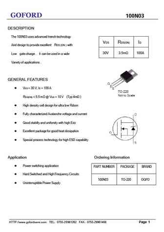
GOFORD 100N03 DESCRIPTION The 100N03 uses advanced trench technology VDS RDS(ON) ID And design to provide excellent RDS (ON ) with 30V 3.5m 100A Low gate charge . It can be used in a wide Vanety of applications . GENERAL FEATURES VDS = 30 V, ID = 100 A RDS(ON)
msk100n03df.pdf
www.msksemi.com MSK100N03DF Semiconductor Compiance Description The MSK100N03DF uses advanced trench technology D D D D to provide excellent RDS(ON), low gate charge and operation with gate voltages as low as 4.5V. This device is suitable for use as a Battery protection or in other Switching application. S S S G General Features DFN3X3-8L VDS = 30V ID =100A RDS(ON)
phb100n03lt-01.pdf
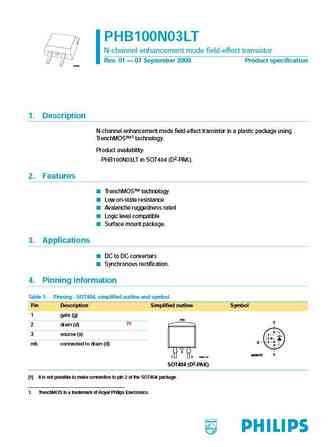
PHB100N03LT N-channel enhancement mode field-effect transistor Rev. 01 07 September 2000 Product specification M3D166 1. Description N-channel enhancement mode field-effect transistor in a plastic package using TrenchMOS 1 technology. Product availability PHB100N03LT in SOT404 (D2-PAK). 2. Features TrenchMOS technology Low on-state resistance Avalanche ruggedness rated
std100n03lt4.pdf
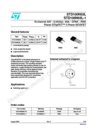
STD100N03L STD100N03L-1 N-channel 30V - 0.0045 - 80A - DPAK - IPAK Planar STripFET II Power MOSFET General features VDSSS RDS(on) ID Type Pw STD100N03L 30 V
rsh100n03tb1.pdf
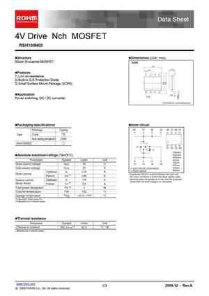
4V Drive Nch MOSFET RSH100N03 Structure Dimensions (Unit mm) Silicon N-channel MOSFET SOP8 Features 1) Low on-resistance. 2) Built-in G-S Protection Diode. 3) Small Surface Mount Package (SOP8). Application Power switching, DC / DC converter. Each lead has same dimensions Packaging specifications Inner circuit (8) (7) (6) (5) (8) (7) (6) (5) Package
rxh100n03.pdf
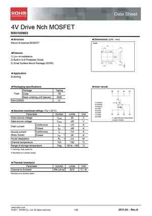
Data Sheet 4V Drive Nch MOSFET RXH100N03 Structure Dimensions (Unit mm) Silicon N-channel MOSFET SOP8 (8) (5) Features 1) Low on-resistance. 2) Built-in G-S Protection Diode. (1) (4) 3) Small Surface Mount Package (SOP8). Application Switching Packaging specifications Inner circuit Package Taping (8) (7) (6) (5) Type Code TB Basic ordering unit (piece
rss100n03fu6tb rss100n03tb.pdf
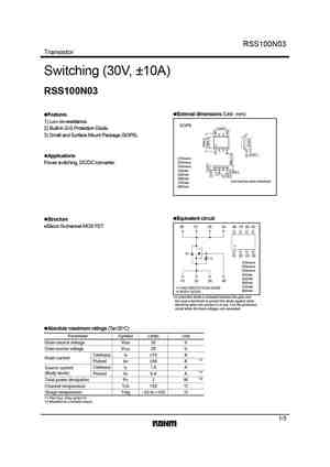
RSS100N03 Transistor Switching (30V, 10A) RSS100N03 External dimensions (Unit mm) Features 1) Low on-resistance. SOP8 5.0 0.2 2) Built-in G-S Protection Diode. 3) Small and Surface Mount Package (SOP8). 0.2 0.1 Applications (1)Source (2)Source Power switching, DC/DC converter. (3)Source (4)Gate 0.4 0.1 1.27 (5)Drain 0.1 (6)Drain Each lead has same dim
sqd100n03-3m4.pdf
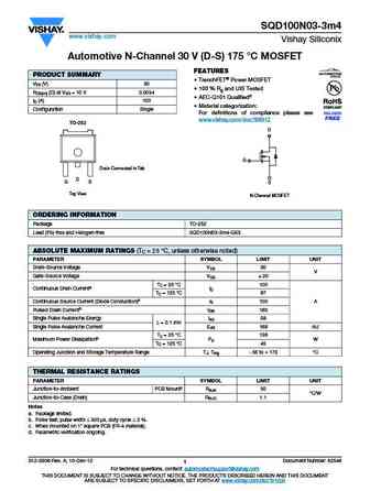
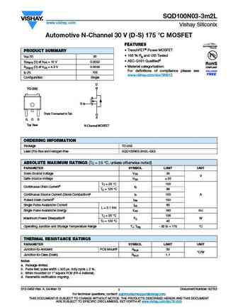
SQD100N03-3m4 www.vishay.com Vishay Siliconix Automotive N-Channel 30 V (D-S) 175 C MOSFET FEATURES PRODUCT SUMMARY TrenchFET Power MOSFET VDS (V) 30 100 % Rg and UIS Tested RDS(on) ( ) at VGS = 10 V 0.0034 AEC-Q101 Qualifiedd ID (A) 100 Material categorization Configuration Single For definitions of compliance please see www.vishay.com/doc?99912 TO-2
sqd100n03-3m2l.pdf
SQD100N03-3m2L www.vishay.com Vishay Siliconix Automotive N-Channel 30 V (D-S) 175 C MOSFET FEATURES TrenchFET Power MOSFET PRODUCT SUMMARY 100 % Rg and UIS Tested VDS (V) 30 AEC-Q101 Qualifiedd RDS(on) ( ) at VGS = 10 V 0.0032 Material categorization RDS(on) ( ) at VGS = 4.5 V 0.0039 For definitions of compliance please see ID (A) 100 www.vishay.com/doc?
bsz100n03msg.pdf
$) $ " $?88, S 07DK >AI A@ D7E;EF3@57 0 D n) G S J57>>7@F 93F7 5 3D97 J BDA6G5F !* ( D n) 1) S , G3>;8;76 355AD6;@9 FA % 8AD F3D97F 3BB>;53F;A@E S .GB7D;AD
bsc100n03msg.pdf
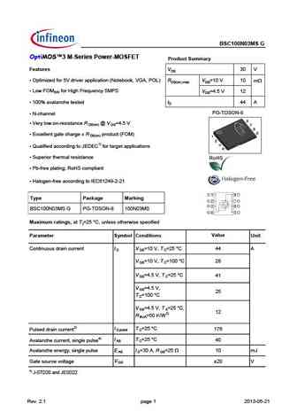
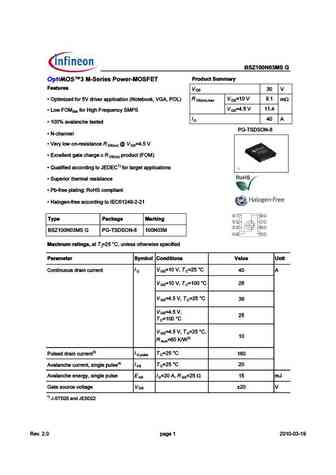
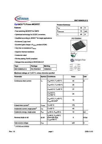
BSC100N03MS G OptiMOS 3 M-Series Power-MOSFET Product Summary Features VDS 30 V Optimized for 5V driver application (Notebook, VGA, POL) RDS(on),max VGS=10 V 10 mW Low FOMSW for High Frequency SMPS VGS=4.5 V 12 100% avalanche tested ID 44 A PG-TDSON-8 N-channel Very low on-resistance R @ V =4.5 V DS(on) GS Excellent gate charge x R product (FOM) DS
bsz100n03lsg.pdf
%* ! % E #;B 1= "% & #=;0@/? %@9 9 -=D Features D Q 2CD CG D49 ?8 ') - . 7@B -'*- 1 m D n) m x 4 Q ) AD > J65 D649?@=@8I 7@B 4@?F6BD6BC D 1) G D ON Q + E2= 7 65 244@B5 ?8 D@ $ 7@B D2B86D 2AA= 42D @?C Q ( 492??6= &@8 4 =6F6= Q H46==6?D 82D6 492B86 H AB@5E4D ) ' D n) Q -EA6B @B D96B>2= B6C CD2?46 Q F2=2?496 B2D65 Q *3 7B66 A=2D ?8 , @"- 4@>A= 2?D Q "2=@86? 7B66
bsc100n03ms.pdf

BSC100N03MS G OptiMOS 3 M-Series Power-MOSFET Product Summary Features VDS 30 V Optimized for 5V driver application (Notebook, VGA, POL) RDS(on),max VGS=10 V 10 mW Low FOMSW for High Frequency SMPS VGS=4.5 V 12 100% avalanche tested ID 44 A PG-TDSON-8 N-channel Very low on-resistance R @ V =4.5 V DS(on) GS Excellent gate charge x R product (FOM) DS
bsc100n03ls.pdf
& " & E $;B1= !#& ' $=;0@/? &@99-=D Features D Q 2CD CG D49 ?8 ') - . 7@B -'*- 1 m D n) m x 44 Q ) AD > J65 D649?@=@8I 7@B 4@?F6BD6BC D 1) Q + E2= 7 65 244@B5 ?8 D@ $ 7@B D2B86D 2AA= 42D @?C G D ON Q ( 492??6= &@8 4 =6F6= Q H46==6?D 82D6 492B86 H AB@5E4D ) ' D n) Q /6BI =@G @? B6C CD2?46 D n) Q -EA6B @B D96B>2= B6C CD2?46 Q F2=2?496 B2D65 Q *3 7B66 A=2D ?8
spb100n03s2-03 spb100n03s2.pdf
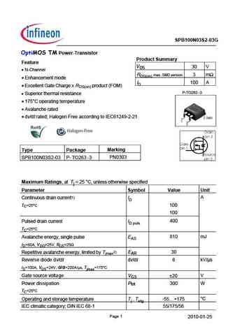
SPB100N03S2-03G OptiMOS TM Power-Transistor Product Summary Feature VDS 30 V N-Channel RDS(on) max. SMD version 3 m Enhancement mode ID 100 A Excellent Gate Charge x RDS(on) product (FOM) P-TO263 -3 Superior thermal resistance 175 C operating temperature Avalanche rated dv/d t rated; Halogen Free according to IEC61249-2-21 Marking Type Package
ut100n03l-ta3-t ut100n03g-ta3-t ut100n03l-tf3-t ut100n03g-tf3-t ut100n03l-tm3-t ut100n03g-tm3-t ut100n03l-tn3-r ut100n03g-tn3-r.pdf

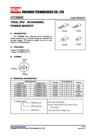
UNISONIC TECHNOLOGIES CO., LTD UT100N03 Power MOSFET 100A, 30V N-CHANNEL POWER MOSFET 1 1 DESCRIPTION TO-220 TO-220F The UT100N03 uses advanced trench technology to provide excellent RDS(ON), low gate charge and operation with low gate voltages. This device is suitable for use as a load 1 1 switch or in PWM applications. TO-252 TO-251 FEATURES 1 * RDS(ON)
ut100n03-q.pdf
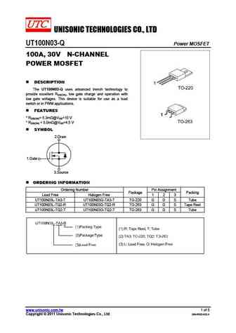
UNISONIC TECHNOLOGIES CO., LTD UT100N03-Q Power MOSFET 100A, 30V N-CHANNEL POWER MOSFET DESCRIPTION The UT100N03-Q uses advanced trench technology to provide excellent RDS(ON), low gate charge and operation with low gate voltages. This device is suitable for use as a load switch or in PWM applications. FEATURES * RDS(ON)= 5.3m @VGS=10 V * RDS(ON) = 8.0m @VGS=4.
ut100n03l-tnd-r ut100n03g-tnd-r ut100n03l-tq2-t ut100n03g-tq2-t ut100n03l-tq2-r ut100n03g-tq2-r ut100n03g-k08-5060-r.pdf
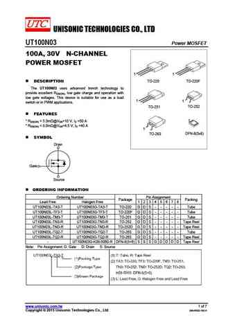
UNISONIC TECHNOLOGIES CO., LTD UT100N03 Power MOSFET 100A, 30V N-CHANNEL POWER MOSFET 1 1 DESCRIPTION TO-220 TO-220F The UT100N03 uses advanced trench technology to provide excellent RDS(ON), low gate charge and operation with low gate voltages. This device is suitable for use as a load 1 1 switch or in PWM applications. TO-252 TO-251 FEATURES 1 * RDS(ON)
g100n03.pdf
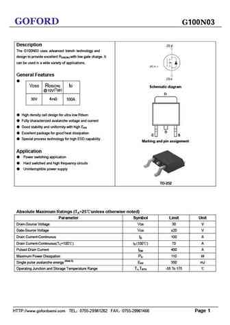
GOFORD G100N03 Description The G100N03 uses advanced trench technology and design to provide excellent RDS(ON) with low gate charge. It can be used in a wide variety of applications. General Features VDSS RDS(ON) ID Schematic diagram @ 10V (Typ) 30V 4m 100A High density cell design for ultra low Rdson Fully characterized avalanche voltage and current
br100n03.pdf
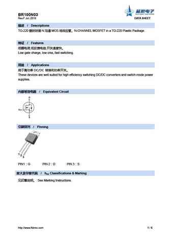
BR100N03 Rev.F Jul.-2018 DATA SHEET / Descriptions TO-220 N MOS N-CHANNEL MOSFET in a TO-220 Plastic Package. / Features , , Low gate charge, low crss, fast switching. / Applications DC/DC These devices are well suited for high efficienc
brb100n03.pdf
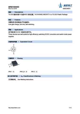
BRB100N03 Rev.A Jul.-2016 DATA SHEET / Descriptions TO-263 N MOS N-CHANNEL MOSFET in a TO-263 Plastic Package. / Features , , Low gate charge, low crss, fast switching. / Applications DC/DC These devices are well suited for high efficien
brcs100n03bd.pdf
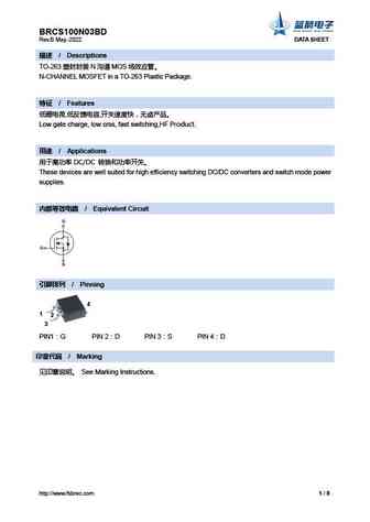
BRCS100N03BD Rev.B May.-2022 DATA SHEET / Descriptions TO-263 N MOS N-CHANNEL MOSFET in a TO-263 Plastic Package. / Features , , Low gate charge, low crss, fast switching,HF Product. / Applications DC/DC These devices ar
brd100n03.pdf
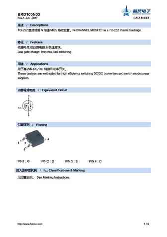
BRD100N03 Rev.A .Jun. -2017 DATA SHEET / Descriptions TO-252 N MOS N-CHANNEL MOSFET in a TO-252 Plastic Package. / Features , , Low gate charge, low crss, fast switching. / Applications DC/DC These devices are well suited for high effici
cs100n03 b4.pdf
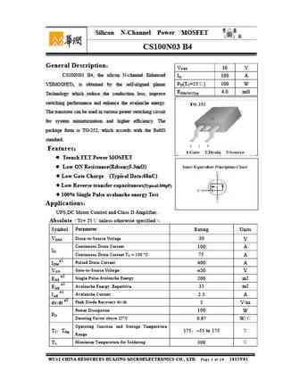
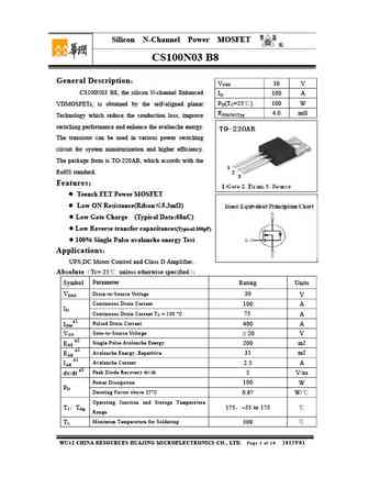
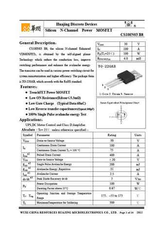
Silicon N-Channel Power MOSFET R CS100N03 B4 General Description VDSS 30 V CS100N03 B4, the silicon N-channel Enhanced ID 100 A PD(TC=25 ) 100 W VDMOSFETs, is obtained by the self-aligned planar RDS(ON)Typ 4.0 m Technology which reduce the conduction loss, improve switching performance and enhance the avalanche energy. The transistor can be used in various
cs100n03f b9.pdf
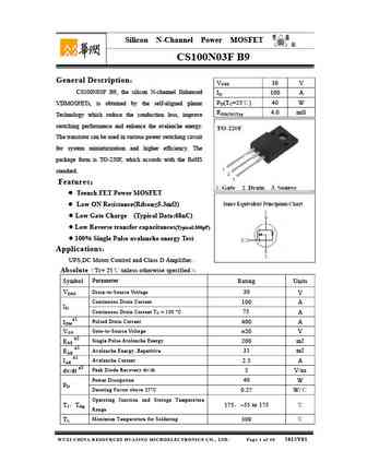
Silicon N-Channel Power MOSFET R CS100N03F B9 General Description VDSS 30 V CS100N03F B9, the silicon N-channel Enhanced ID 100 A PD(TC=25 ) 40 W VDMOSFETs, is obtained by the self-aligned planar RDS(ON)Typ 4.0 m Technology which reduce the conduction loss, improve switching performance and enhance the avalanche energy. The transistor can be used in various
cs100n03 b8.pdf
Silicon N-Channel Power MOSFET R CS100N03 B8 General Description VDSS 30 V CS100N03 B8, the silicon N-channel Enhanced ID 100 A PD(TC=25 ) 100 W VDMOSFETs, is obtained by the self-aligned planar RDS(ON)Typ 4.0 m Technology which reduce the conduction loss, improve switching performance and enhance the avalanche energy. The transistor can be used in various pow
cm100n03.pdf
R CM100N03 www.jdsemi.cn ShenZhen Jingdao Electronic Co.,Ltd. POWER MOSFET 30V N-Channel Trench-MOS RoHS 1 US P 2 3
dh100n03b13 dhf100n03b13 dhi100n03b13 dhe100n03b13 dhb100n03b13 dhd100n03b13.pdf
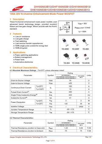
DH100N03B13/DHF100N03B13/DHI100N03B13/ DHE100N03B13/DHB100N03B13/DHD100N03B13 100A 30V N-channel Enhancement Mode Power MOSFET 1 Description These N-channel enhancement mode power mosfets used 2 D V = 30V DSS advanced trench technology design, provided excellent Rdson and low gate charge. Which accords with the RoHS G R = 3.3m DS(on) (TYP) standard. 1 3 S I = 100A D 2 Featur
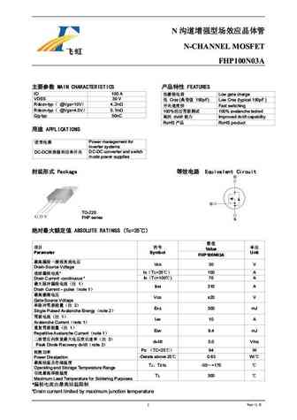
fhu100n03c fhd100n03c fhp100n03c.pdf

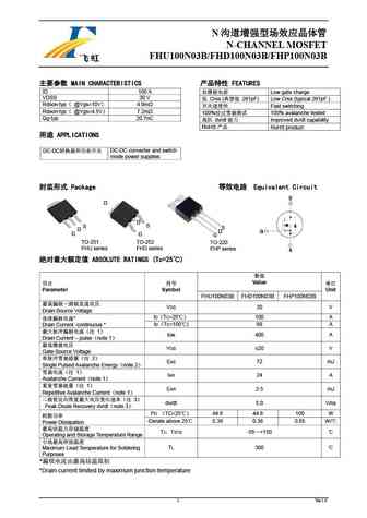
N N-CHANNEL MOSFET FHU100N03C/FHD100N03C/FHP100N03C MAIN CHARACTERISTICS FEATURES ID 100 A Low gate charge VDSS 30 V Crss ( 261pF) Low Crss (typical 261pF ) Rdson-typ @Vgs=10V 3.7m Fast switching Rdson-typ @Vgs=4.5V 5.1m 100% 100% avala
fhu100n03b fhd100n03b fhp100n03b.pdf
N N-CHANNEL MOSFET FHU100N03B/FHD100N03B/FHP100N03B MAIN CHARACTERISTICS FEATURES ID 100 A Low gate charge VDSS 30 V Crss ( 261pF) Low Crss (typical 261pF ) Rdson-typ @Vgs=10V 4.9m Fast switching Rdson-typ @Vgs=4.5V 7.2m 100% 100% avala
me100n03t me100n03t-g.pdf
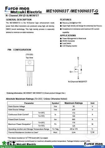
ME100N03T /ME100N03T-G N- Channel 30V (D-S) MOSFET GENERAL DESCRIPTION FEATURES The ME100N03T-G is the N-Channel logic enhancement mode RDS(ON) 3m @VGS=10V power field effect transistors are produced using high cell density, Super high density cell design for extremely low RDS(ON) DMOS trench technology. This high density process is especially Exceptional on-resistance
sl100n03r.pdf
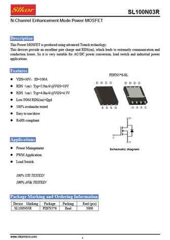
SL100N03R N-Channel Enhancement Mode Power MOSFET Description This Power MOSFET is produced using advanced Trench technology. This devices provide an excellent gate charge and RDS(on), which leads to extremely communication and conduction losses. So it is very suitable for AC/DC power conversion, load switch and industrial power applications. Features PDFN5*6-8L VDS=30V I
100n03a.pdf
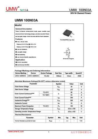
R UMW UMW 100N03A 30V N-Channel Power UMW 100N03A Mosfet General Description These N-channel enhancement mode power mosfets used advanced trench technology design, provided excellent Rdson and low gate charge. Which accords with the RoHS standard. Features VDS = 30V,ID =90A RDS(ON),3.8 m (Typ) @ VGS =10V RDS(ON), 6.4m (Typ) @ VGS =4.5V Low on resistance Low gate charge Fast s
cs100n03b8.pdf
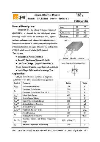
Huajing Discrete Devices R Silicon N-Channel Power MOSFET CS100N03 B8 General Description VDSS 30 V CS100N03 B8, the silicon N-channel Enhanced ID 100 A PD(TC=25 ) 100 W VDMOSFETs, is obtained by the self-aligned planar RDS(ON)Typ 4.0 m Technology which reduce the conduction loss, improve switching performance and enhance the avalanche energy. The transist
cs100n03b4.pdf
Huajing Discrete Devices R Silicon N-Channel Power MOSFET CS100N03 B4 General Description VDSS 30 V CS100N03 B4, the silicon N-channel Enhanced ID 100 A PD(TC=25 ) 100 W VDMOSFETs, is obtained by the self-aligned planar RDS(ON)Typ 4.0 m Technology which reduce the conduction loss, improve switching performance and enhance the avalanche energy. The transist
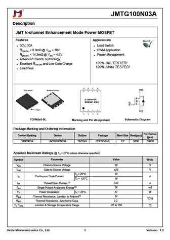
jmtg100n03a.pdf
JMTG100N03A Description JMT N-channel Enhancement Mode Power MOSFET Features Applications 30V, 30A Load Switch RDS(ON)
jmtk100n03a.pdf
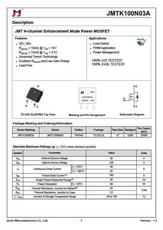
JMTK100N03A Description JMT N-channel Enhancement Mode Power MOSFET Features Applications 30V, 40A Load Switch RDS(ON)
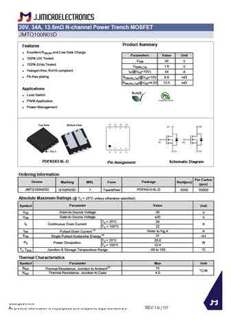
jmtq100n03a.pdf
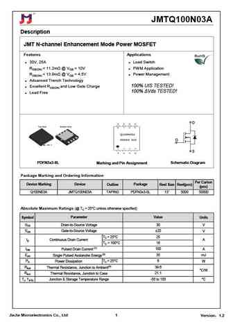
JMTQ100N03A Description JMT N-channel Enhancement Mode Power MOSFET Features Applications 30V, 25A Load Switch RDS(ON)
vbzm100n03.pdf
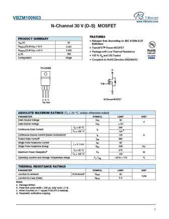
VBZM100N03 www.VBsemi.com N-Channel 30 V (D-S) MOSFET FEATURES PRODUCT SUMMARY Halogen-free According to IEC 61249-2-21 VDS (V) 30 Definition RDS(on) ( ) at VGS = 10 V 0.001 TrenchFET Power MOSFET RDS(on) ( ) at VGS = 4.5 V 0.002 Package with Low Thermal Resistance ID (A) 260 100 % Rg and UIS Tested Configuration Single Compliant to RoHS Directive 20
vbze100n03.pdf
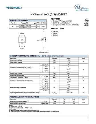
VBZE100N03 www.VBsemi.com N-Channel 30-V (D-S) MOSFET FEATURES PRODUCT SUMMARY TrenchFET Power MOSFET VDS (V) RDS(on) ( ) ID (A)a, e Qg (Typ) 100 % Rg and UIS Tested Compliant to RoHS Directive 2011/65/EU 0.0092at VGS = 10 V 60 30 31 nC 0.011 at VGS = 4.5 V 50 APPLICATIONS D OR-ing TO-252 Server DC/DC G G D S Top View S N-Channel MOSFET ABS
rss100n03t.pdf
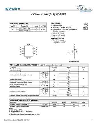
RSS100N03T www.VBsemi.tw N-Channel 20V (D-S) MOSFET FEATURES PRODUCT SUMMARY Halogen-free VDS (V) RDS(on) ( ) ID (A)a Qg (Typ.) TrenchFET Power MOSFET 0.012 at VGS = 10 V 12 20 6.1 nC Optimized for High-Side Synchronous 0.015 at VGS = 4.5 V 11 Rectifier Operation 100 % Rg Tested 100 % UIS Tested APPLICATIONS Notebook CPU Core - High-Side Switch
ut100n03l.pdf
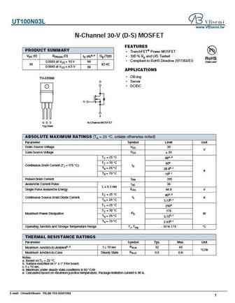
UT100N03L www.VBsemi.tw N-Channel 30-V (D-S) MOSFET FEATURES PRODUCT SUMMARY TrenchFET Power MOSFET VDS (V) RDS(on) ( ) ID (A)a, e Qg (Typ) 100 % Rg and UIS Tested Compliant to RoHS Directive 2011/65/EU 0.0035 at VGS = 10 V 98 30 82 nC 0.0045 at VGS = 4.5 V 98 APPLICATIONS OR-ing TO-220AB D Server DC/DC G S G D S N-Channel MOSFET Top View AB
hm100n03.pdf
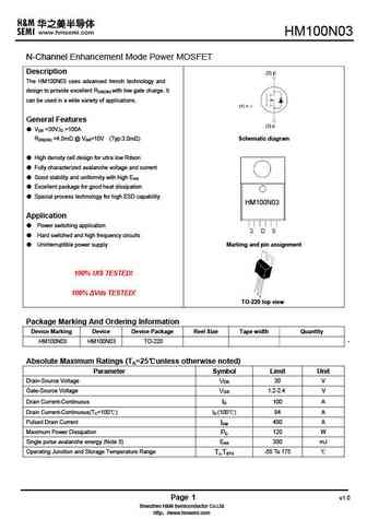
HM100N03 N-Channel Enhancement Mode Power MOSFET Description The HM100N03 uses advanced trench technology and design to provide excellent RDS(ON) with low gate charge. It can be used in a wide variety of applications. General Features VDS =30V,ID =100A RDS(ON)
hm100n03k.pdf
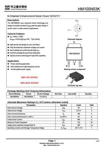
HM100N03K N-Channel Enhancement Mode Power MOSFET Description The HM100N03K uses advanced trench technology and design to provide excellent RDS(ON) with low gate charge. It can be used in a wide variety of applications. General Features VDS =30V,ID =100A RDS(ON)
hm100n03d.pdf
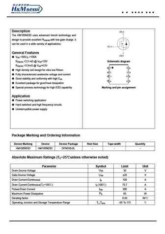
HM100N03D Description The HM100N03D uses advanced trench technology and design to provide excellent RDS(ON) with low gate charge. It can be used in a wide variety of applications. General Features VDS =30V,ID =100A RDS(ON)
mpg100n03p.pdf
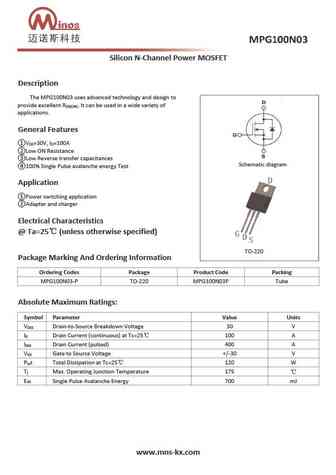
Silicon N-Channel Power MOSFET Description The MPG100N03 uses advanced technology and design to provide excellent R . It can be used in a wide variety of DS(ON) applications. General Features V =30V, I =100A DS D Low ON Resistance Low Reverse transfer capacitances Schematic diagram 100% Single Pulse avalanche energy Test Application Power switching application A
ap100n03p ap100n03t.pdf
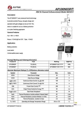
AP100N03P/T 30V N-Channel Enhancement Mode MOSFET Description The AP100N03P/T uses advanced trench technology to provide excellent R , low gate charge and DS(ON) operation with gate voltages as low as 4.5V. This device is suitable for use as a Battery protection or in other Switching application. General Features V = 30V I =100 A DS D R
ap100n03ad.pdf
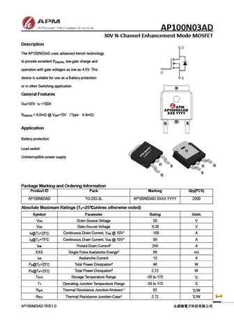
AP100N03AD 30V N-Channel Enhancement Mode MOSFET Description The AP100N03AD uses advanced trench technology to provide excellent R , low gate charge and DS(ON) operation with gate voltages as low as 4.5V. This device is suitable for use as a Battery protection or in other Switching application. General Features V =30V I =100A DS D R
ap100n03d.pdf
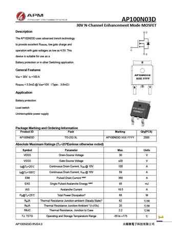
AP100N03D 30V N-Channel Enhancement Mode MOSFET Description The AP100N03D uses advanced trench technology to provide excellent R , low gate charge and DS(ON) operation with gate voltages as low as 4.5V. This device is suitable for use as a Battery protection or in other Switching application. General Features V = 30V I =100 A DS D R
ap100n03y.pdf
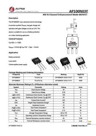
AP100N03Y 30V N-Channel Enhancement Mode MOSFET Description The AP100N03Y uses advanced trench technology to provide excellent R , low gate charge and DS(ON) operation with gate voltages as low as 4.5V. This device is suitable for use as a Battery protection or in other Switching application. General Features V =30V I =100A DS D R
Другие MOSFET... GD1 , G22 , G23 , G11 , G16 , G17 , 03N06 , 05N06 , 7N65 , 100P03 , 10N03 , 110N10 , 11N10C , 120N03 , 1402TR , 1404TR , 140N10 .


Список транзисторов
Обновления
MOSFET: AOI780A70 | AOB42S60L | AOTF950A70L | AOTF27S60L | AOTF11S60L | AONV070V65G1 | AOM065V120X2Q | AOM033V120X2 | AOK500V120X2 | AOK065V65X2 | AOK065V120X2 | AOK033V120X2Q | AOK033V120X2 | AOB380A60L | AOB29S50L | AO3481C
Popular searches
irf3205 reemplazo | mpsu06 | кт630 | 2g381 transistor | 2sc2383 transistor equivalent | 2sd669 transistor | 75n65kdf | c2274 transistor