140N10. Аналоги и основные параметры
Наименование производителя: 140N10
Тип транзистора: MOSFET
Полярность: N
Предельные значения
Pd ⓘ - Максимальная рассеиваемая мощность: 215 W
|Vds|ⓘ - Максимально допустимое напряжение сток-исток: 100 V
|Vgs|ⓘ - Максимально допустимое напряжение затвор-исток: 25 V
|Id| ⓘ - Максимально допустимый постоянный ток стока: 140 A
Tj ⓘ - Максимальная температура канала: 175 °C
Электрические характеристики
tr ⓘ - Время нарастания: 116 ns
Cossⓘ - Выходная емкость: 942 pf
RDSonⓘ - Сопротивление сток-исток открытого транзистора: 0.0072 Ohm
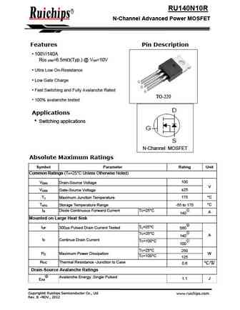
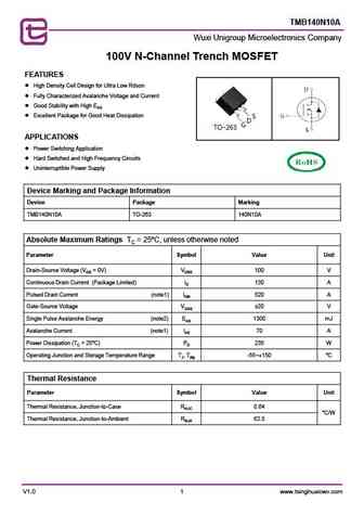
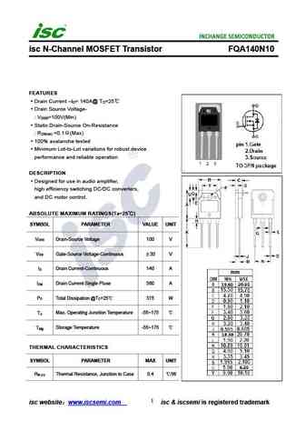
Тип корпуса: TO220
Аналог (замена) для 140N10
- подборⓘ MOSFET транзистора по параметрам
140N10 даташит
140n10.pdf
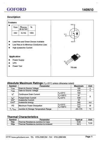
GOFORD 140N10 Description Features VDSS RDS(ON) ID @ 10V (typ) 100V m 6.2 140A Lead free and Green Device Available Low Rds-on to Minimize Conductive Loss High avalanche Current Application Power Supply UPS Power Tool TO-220 Absolute Maximum Ratings (TA=25 C unless otherwise noted) Symbol Parameter Maximum Unit VDSS Drain-to-Source V
fqh140n10.pdf
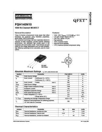
TM QFET FQH140N10 100V N-Channel MOSFET General Description Features These N-Channel enhancement mode power field effect 140A, 100V, RDS(on) = 0.01 @VGS = 10 V transistors are produced using Fairchild s proprietary, Low gate charge ( typical 220 nC) planar stripe, DMOS technology. Low Crss ( typical 470 pF) This advanced technology has been especially tailored to
fqa140n10.pdf
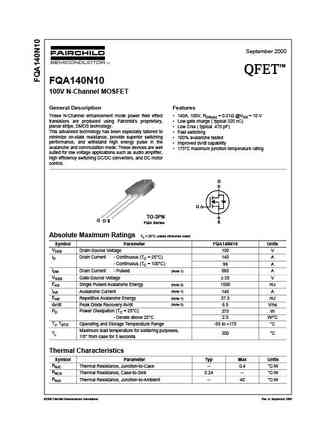
September 2000 TM QFET QFET QFET QFET FQA140N10 100V N-Channel MOSFET General Description Features These N-Channel enhancement mode power field effect 140A, 100V, RDS(on) = 0.01 @VGS = 10 V transistors are produced using Fairchild s proprietary, Low gate charge ( typical 220 nC) planar stripe, DMOS technology. Low Crss ( typical 470 pF) This advanced technology has
ixtq140n10p ixtt140n10p.pdf
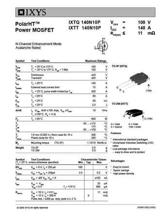
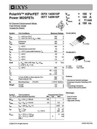
IXTQ 140N10P VDSS = 100 V PolarHTTM IXTT 140N10P ID25 = 140 A Power MOSFET RDS(on) 11 m N-Channel Enhancement Mode Avalanche Rated Symbol Test Conditions Maximum Ratings TO-3P (IXTQ) VDSS TJ = 25 C to 175 C 100 V VDGR TJ = 25 C to 175 C; RGS = 1 M 100 V VGS Continuous 20 V VGSM Transient 30 V ID25 TC = 25 C 140 A ID(RMS)

Другие MOSFET... 100N03 , 100P03 , 10N03 , 110N10 , 11N10C , 120N03 , 1402TR , 1404TR , IRF9540N , ECYA , G1002 , G1002L , G1003A , G1006 , G1006A , G1008 , G2002 .
History: G1003A | 05N06
🌐 : EN ES РУ

Список транзисторов
Обновления
MOSFET: ASB80R750E | ASB70R380E | ASB65R300E | ASB65R220E | ASB65R120EFD | ASB60R150E | ASA80R900E | ASA80R750E | ASA80R290E | ASA70R950E | ASA70R600E | ASA70R380E | ASA70R240E | ASA65R850E | ASA65R550E | ASA65R350E
Popular searches
c5200 2sc5200 transistor datasheet | d2390 datasheet | 2sa750 replacement | 2sc984 replacement | a1046 transistor | hy19p03 | 2sk2749 | c2577 transistor