16N10. Аналоги и основные параметры
Наименование производителя: 16N10
Тип транзистора: MOSFET
Полярность: N
Предельные значения
Pd ⓘ
- Максимальная рассеиваемая мощность: 50 W
|Vds|ⓘ - Максимально допустимое напряжение сток-исток: 100 V
|Vgs|ⓘ - Максимально допустимое напряжение затвор-исток: 20 V
|Id| ⓘ - Максимально допустимый постоянный ток стока: 15 A
Tj ⓘ - Максимальная температура канала: 175 °C
Электрические характеристики
tr ⓘ -
Время нарастания: 6.5 ns
Cossⓘ - Выходная емкость: 160 pf
RDSonⓘ - Сопротивление сток-исток открытого транзистора: 0.08 Ohm
Тип корпуса: TO252
Аналог (замена) для 16N10
- подборⓘ MOSFET транзистора по параметрам
16N10 даташит
..1. Size:1601K goford
16n10.pdf 
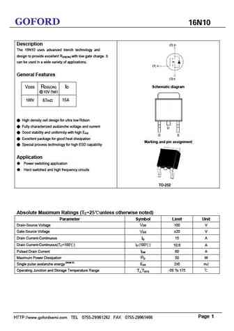
GOFORD 16N10 Description The 16N10 uses advanced trench technology and design to provide excellent RDS(ON) with low gate charge. It can be used in a wide variety of applications. General Features Schematic diagram VDSS RDS(ON) ID @ 10V (typ) 15A 100V 67m High density cell design for ultra low Rdson Fully characterized avalanche voltage and current Good s
0.2. Size:50K st
stp16n10l.pdf 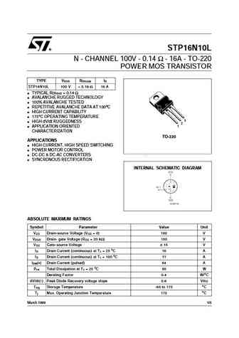
STP16N10L N - CHANNEL 100V - 0.14 - 16A - TO-220 POWER MOS TRANSISTOR TYPE VDSS RDS(on) ID STP16N10L 100 V
0.4. Size:269K infineon
ipg16n10s4l-61a.pdf 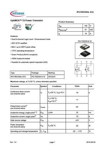
IPG16N10S4L-61A OptiMOS -T2 Power-Transistor Product Summary VDS 100 V RDS(on),max3) 61 mW ID 16 A Features Dual N-channel Logic Level - Enhancement mode PG-TDSON-8-10 AEC Q101 qualified MSL1 up to 260 C peak reflow 175 C operating temperature Green Product (RoHS compliant) 100% Avalanche tested Feasible for automatic optical inspection (AOI) Type
0.5. Size:195K infineon
ipg16n10s4-61a.pdf 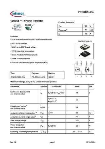
IPG16N10S4-61A OptiMOS -T2 Power-Transistor Product Summary VDS 100 V RDS(on),max3) 61 m ID 16 A Features Dual N-channel Normal Level - Enhancement mode PG-TDSON-8-10 AEC Q101 qualified MSL1 up to 260 C peak reflow 175 C operating temperature Green Product (RoHS compliant) 100% Avalanche tested Feasible for automatic optical inspection (AOI) Typ
0.6. Size:172K ixys
ixth16n10d2 ixtt16n10d2.pdf 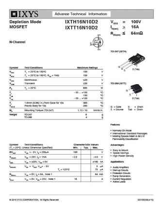
Advance Technical Information Depletion Mode VDSX = 100V IXTH16N10D2 MOSFET ID(on) > 16A IXTT16N10D2 RDS(on) 64m N-Channel TO-247 (IXTH) G Symbol Test Conditions Maximum Ratings D D (Tab) S VDSX TJ = 25 C to 150 C 100 V VDGX TJ = 25 C to 150 C, RGS = 1M 100 V VGSX Continuous 20 V VGSM Transient 30 V TO-268 (IXTT) PD TC = 25 C 695
0.7. Size:645K cet
cep16n10l ceb16n10l.pdf 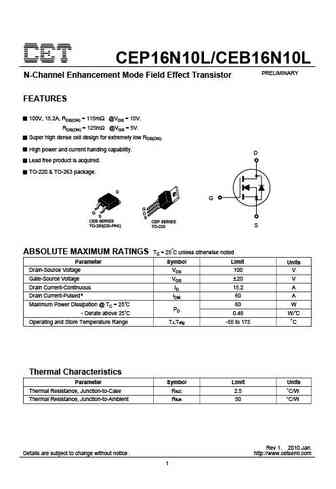
CEP16N10L/CEB16N10L PRELIMINARY N-Channel Enhancement Mode Field Effect Transistor FEATURES 100V, 15.2A, RDS(ON) = 115m @VGS = 10V. RDS(ON) = 125m @VGS = 5V. Super high dense cell design for extremely low RDS(ON). High power and current handing capability. D Lead free product is acquired. TO-220 & TO-263 package. G CEB SERIES CEP SERIES TO-263(DD-PAK) S TO-220 ABSOLUTE MA
0.8. Size:623K cet
ceu16n10 ced16n10.pdf 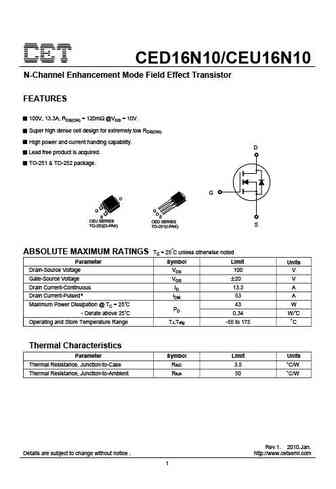
CED16N10/CEU16N10 N-Channel Enhancement Mode Field Effect Transistor FEATURES 100V, 13.3A, RDS(ON) = 120m @VGS = 10V. Super high dense cell design for extremely low RDS(ON). High power and current handing capability. D Lead free product is acquired. TO-251 & TO-252 package. G D G S CEU SERIES CED SERIES S TO-252(D-PAK) TO-251(I-PAK) ABSOLUTE MAXIMUM RATINGS Tc = 25 C unless
0.9. Size:684K cet
ceu16n10l ced16n10l.pdf 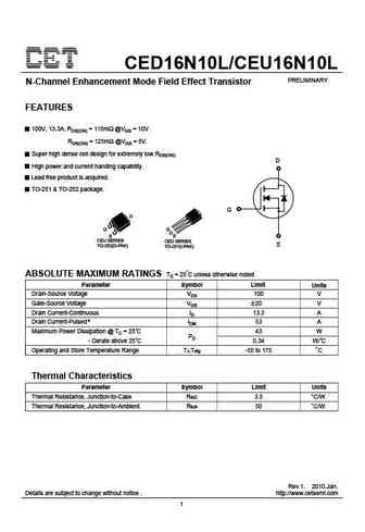
CED16N10L/CEU16N10L PRELIMINARY N-Channel Enhancement Mode Field Effect Transistor FEATURES 100V, 13.3A, RDS(ON) = 115m @VGS = 10V. RDS(ON) = 125m @VGS = 5V. Super high dense cell design for extremely low RDS(ON). D High power and current handing capability. Lead free product is acquired. TO-251 & TO-252 package. G D G S CEU SERIES CED SERIES S TO-252(D-PAK) TO-251(I-P
0.10. Size:534K cet
cep16n10 ceb16n10.pdf 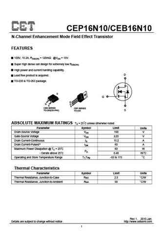
CEP16N10/CEB16N10 N-Channel Enhancement Mode Field Effect Transistor FEATURES 100V, 15.2A, RDS(ON) = 120m @VGS = 10V. Super high dense cell design for extremely low RDS(ON). High power and current handing capability. D Lead free product is acquired. TO-220 & TO-263 package. G CEB SERIES CEP SERIES TO-263(DD-PAK) S TO-220 ABSOLUTE MAXIMUM RATINGS Tc = 25 C unless otherwise noted
0.11. Size:112K ssdi
sff116n10m sff116n10z.pdf 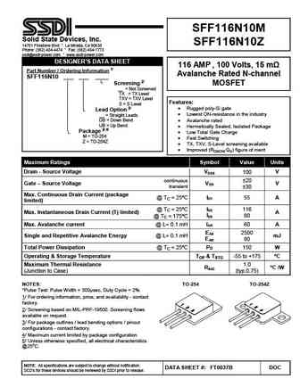
SFF116N10M Solid State Devices, Inc. SFF116N10Z 14701 Firestone Blvd * La Mirada, Ca 90638 Phone (562) 404-4474 * Fax (562) 404-1773 ssdi@ssdi-power.com * www.ssdi-power.com DESIGNER S DATA SHEET 116 AMP , 100 Volts, 15 m Part Number / Ordering Information 1/ Avalanche Rated N-channel SFF116N10 ___ ___ ____ Screening 2/ MOSFET __ = Not Scre
0.12. Size:1307K belling
blm16n10-p blm16n10-d.pdf 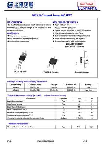
Green Product BLM16N10 100V N-Channel Power MOSFET DESCRIPTION KEY CHARACTERISTICS The BLM16N10 uses advanced trench technology to provide V = 100V,I = 60A DS D excellent R , low gate charge. It can be used in a wide R
0.13. Size:803K ncepower
ncep016n10ll.pdf 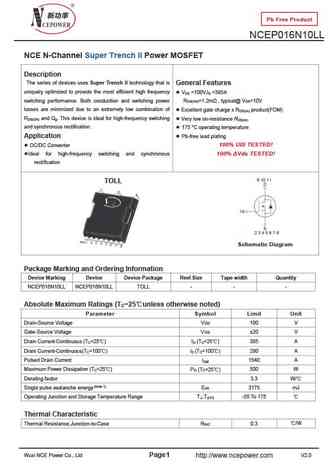
Pb Free Product NCEP016N10LL NCE N-Channel Super Trench II Power MOSFET Description The series of devices uses Super Trench II technology that is General Features uniquely optimized to provide the most efficient high frequency V =100V,I =385A DS D switching performance. Both conduction and switching power R =1.2m , typical@ V =10V DS(ON) GS losses are minimized due to an extrem
0.14. Size:597K ncepower
nceap016n10ll.pdf 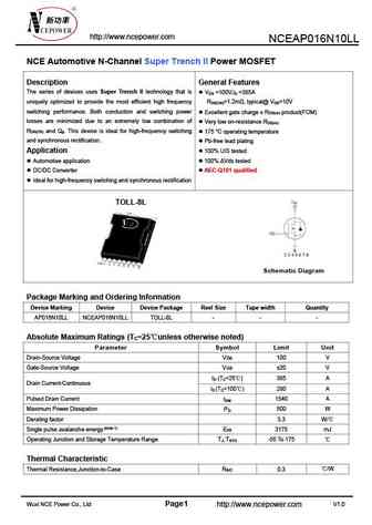
http //www.ncepower.com NCEAP016N10LL NCE Automotive N-Channel Super Trench II Power MOSFET Description General Features The series of devices uses Super Trench II technology that is V =100V,I =385A DS D uniquely optimized to provide the most efficient high frequency R =1.2m , typical@ V =10V DS(ON) GS switching performance. Both conduction and switching power Excellent gate
0.15. Size:1056K stansontech
st16n10.pdf 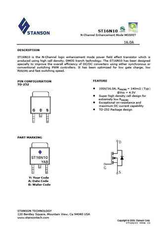
ST16N10 N Channel Enhancement Mode MOSFET 16.0A DESCRIPTION ST16N10 is the N-Channel logic enhancement mode power field effect transistor which is produced using high cell density, DMOS trench technology. The ST16N10 has been designed specially to improve the overall efficiency of DC/DC converters using either synchronous or conventional switching PWM controllers. It has been opt
0.16. Size:643K way-on
wmk16n10t1.pdf 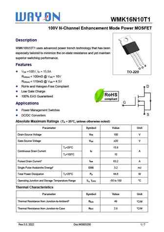
WMK16N10T1 100V N-Channel Enhancement Mode Power MOSFET Description WMK16N10T1 uses advanced power trench technology that has been especially tailored to minimize the on-state resistance and yet maintain superior switching performance. Features S D G V =100V, I = 15.8A DS D TO-220 R
0.17. Size:4770K haolin elec
hp16n10 hf16n10.pdf 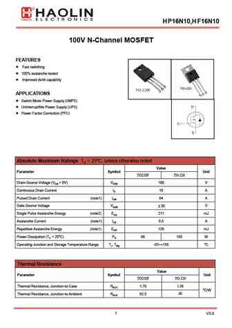
H P16N10,H F16N10 100V N-Channel MOSFET FEATURES Fast switching 100% avalanche tested Improved dv/dt capability APPLICATIONS Switch Mode Power Supply (SMPS) Uninterruptible Power Supply (UPS) Power Factor Correction (PFC) Absolute Maximum Ratings TC = 25 unless otherwise noted C, Value Parameter Symbol Unit TO220F TO-220 Drain-Source Voltage (VGS = 0V) V
0.18. Size:1154K cn agmsemi
agm16n10c.pdf 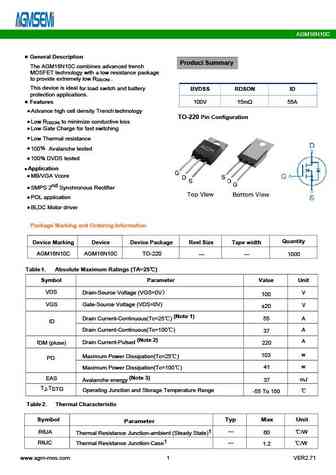
AGM16N10C General Description Product Summary The AGM16N10C combines advanced trench MOSFET technology with a low resistance package to provide extremely low R . DS(ON) This device is ideal for load switch and battery BVDSS RDSON ID protection applications. Features 100V 15m 55A Advance high cell density Trench technology TO-220 Pin Configuration Low R to minimi
0.19. Size:1182K cn agmsemi
agm16n10d.pdf 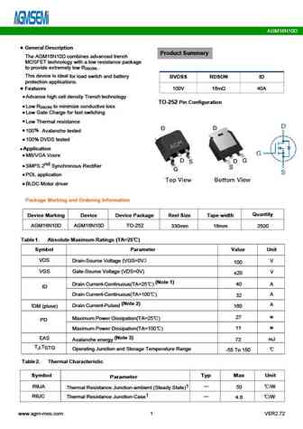
AGM16N10D General Description Product Summary The AGM16N10D combines advanced trench MOSFET technology with a low resistance package to provide extremely low R . DS(ON) This device is ideal for load switch and battery BVDSS RDSON ID protection applications. Features 100V 16m 40A Advance high cell density Trench technology TO-252 Pin Configuration Low R to minimi
0.20. Size:1148K winsok
wsp16n10.pdf 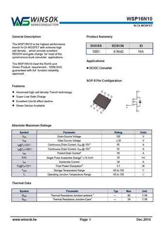
WSP16N10 N-Ch MOSFET General Description Product Summery The WSP16N10 is the highest performance BVDSS RDSON ID trench N-Ch MOSFET with extreme high cell density , which provide excellent 100V 8.9m 16A RDSON and gate charge for most of the synchronous buck converter applications . Applications The WSF16N10 meet the RoHS and Green Product requirement , 100% EAS DC/DC
Другие MOSFET... G110N06
, G120N04
, G120N04A
, G15P04
, G1815
, G1816
, G1825
, 15P03
, 10N65
, 18N10
, 2002A
, 20P10
, 21N06
, 22N10
, 2301H
, 2301L
, 25P06
.