8205A datasheet, аналоги, основные параметры
8205A - это популярный двойной N-канальный МОП-транзистор, обычно используемый в компактных схемах управления питанием, особенно в платах защиты литий-ионных аккумуляторов. Он объединяет два МОП-транзистора в одном корпусе SOT23-6, обеспечивая эффективное переключение на высокую или низкую мощность в условиях ограниченного пространства на печатной плате. Устройство обычно оснащено низким Rds(on), что сводит к минимуму потери проводимости и тепловыделение при работе на высоких токах. Номинальное напряжение питания от источника питания составляет около 20В, а постоянный ток разряда составляет 4А, что делает его пригодным для портативной электроники, преобразователей постоянного тока в постоянный, переключателей нагрузки, конструкций BMS с батарейными блоками. 8205A также обладает характеристиками быстрой коммутации благодаря низкому заряду затвора, что повышает общую эффективность системы. Интеграция двух согласованных МОП-транзисторов упрощает проектирование схемы, сокращает количество компонентов и повышает надежность в компактных системах электропитания.
Наименование производителя: 8205A 📄📄
Тип транзистора: MOSFET
Полярность: N
Предельные значения
Pd ⓘ - Максимальная рассеиваемая мощность: 1.25 W
|Vds|ⓘ - Максимально допустимое напряжение сток-исток: 20 V
|Vgs|ⓘ - Максимально допустимое напряжение затвор-исток: 10 V
|Id| ⓘ - Максимально допустимый постоянный ток стока: 4 A
Tj ⓘ - Максимальная температура канала: 150 °C
Электрические характеристики
tr ⓘ - Время нарастания: 14 ns
Cossⓘ - Выходная емкость: 115 pf
RDSonⓘ - Сопротивление сток-исток открытого транзистора: 0.025 Ohm
Тип корпуса: SOT23-6
📄📄 Копировать
Аналог (замена) для 8205A
- подборⓘ MOSFET транзистора по параметрам
8205A даташит
..1. Size:1693K goford
8205a.pdf 
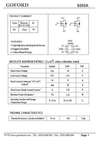
GOFORD 8205A PR ODUC T S UMMAR Y D1 D2 - VDSS RDS(ON) ID G 1 G 2 @ (typ) 4.0V 4A 20V 21m S 1 S 2 S OT26 F E ATUR E S Top View S uper high dense cell design for low R DS (ON). S 1 G1 6 1 R ugged and reliable. D1/D2 2 5 D1/D2 3 4 S 2 G2 S urface Mount Package. ABS OLUTE MAXIMUM R ATINGS (TA=25 C unless otherwise noted) Limit Unit Parameter S ymbol Drain-S ou
..2. Size:695K umw-ic
8205a.pdf 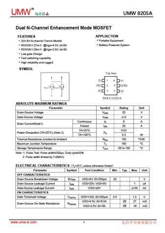
R UMW UMW 8205A UMW 8205A Dual N-Channel Enhancement Mode MOSFET APPLIACTION FEATURES Portable Equipment 20V 5A N-channel Trench Mosfet Battery Powered System RDSON 27m @Vgs=4.5V, Id=5A RDSON 36m @Vgs=2.5V, Id=3A Low gate Charge Fast switching capability High reliability and rugged SYMBOL ABSOLUTE MAXIMUM RATINGS Parameter Symbol Rating Unit Drain-
..3. Size:1989K guangdong hottech
8205a.pdf 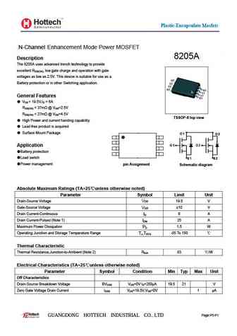
Plastic-Encapsulate Mosfets N-Channel Enhancement Mode Power MOSFET 8205A Description The 8205A uses advanced trench technology to provide excellent RDS(ON), low gate charge and operation with gate voltages as low as 2.5V. This device is suitable for use as a Battery protection or in other Switching application. General Features VDS = 19.5V,ID = 6A RDS(ON)
..4. Size:177K jsmsemi
8205a 8205s.pdf 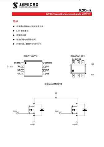
8205-A 20V N-Channel Enhancement-Mode MOSFET 2.5V TSSOP-8/SOT-23-6 8205A/TSSOP-8 8205S/SOT-23-6 G1 NC G2 6 5 4 D1/D2 8 D1/D2 S1 D S2 S1 7 S2 S1 6 S2 G1 5 G2 Drain 1 2 3 N-Channel MOSFET Gate1 Gate2 So
..5. Size:1264K cn alj
8205a.pdf 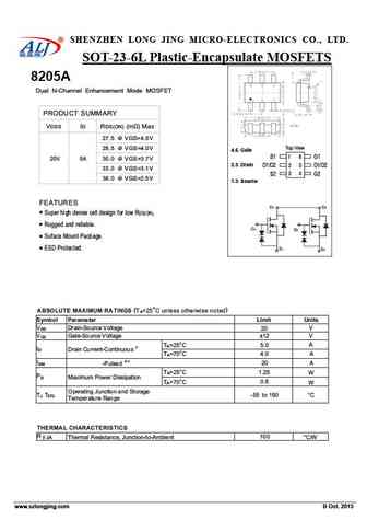
SHENZHEN LONG JING MICRO-ELECTRONICS CO., LTD. SOT-23-6L Plastic-Encapsulate MOSFETS 8205A Dual N-Channel Enhancement Mode MOSFET PRODUCT SUMMARY VDSS ID RDS(ON) (m ) Max 27.5 @ VGS=4.5V Top View 28.5 @ VGS=4.0V 4.6. Gate S1 1 6 G1 20V 5A 30.0 @ VGS=3.7V 2.5. Drain 2 5 D1/D2 D1/D2 33.0 @ VGS=3.1V 3 4 S2 G2 38.0 @ VGS=2.5V 1.3. Source FEATURES D1 D2 Super high d
0.1. Size:115K onsemi
ngd8205a.pdf 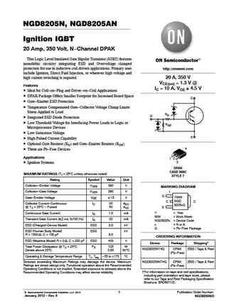
NGD8205N, NGD8205AN Ignition IGBT 20 Amp, 350 Volt, N-Channel DPAK This Logic Level Insulated Gate Bipolar Transistor (IGBT) features monolithic circuitry integrating ESD and Overvoltage clamped protection for use in inductive coil drivers applications. Primary uses http //onsemi.com include Ignition, Direct Fuel Injection, or wherever high voltage and high current switching is required
0.2. Size:420K utc
ut8205al-al6-r ut8205ag-ag6-r ut8205al-s08-r ut8205ag-s08-r ut8205al-p08-r ut8205ag-p08-r.pdf 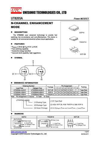
UNISONIC TECHNOLOGIES CO., LTD UT8205A Power MOSFET N-CHANNEL ENHANCEMENT MODE DESCRIPTION The UT8205A uses advanced technology to provide fast switching, low on-resistance and cost-effectiveness. This device is suitable for all commercial-industrial surface mount applications. FEATURES * RDS(ON) 28m @ VGS=4.5V, ID=6.0A * Fast switching capability * Avalanch
0.3. Size:217K utc
ut8205a.pdf 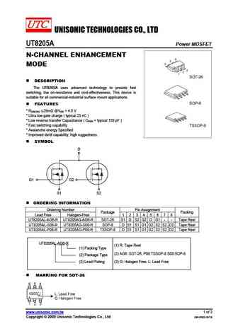
UNISONIC TECHNOLOGIES CO., LTD UT8205A Power MOSFET N-CHANNEL ENHANCEMENT MODE DESCRIPTION The UT8205A uses advanced technology to provide fast switching, low on-resistance and cost-effectiveness. This device is suitable for all commercial-industrial surface mount applications. FEATURES * RDS(ON) 28m @VGS = 4.5 V * Ultra low gate charge ( typical 23 nC ) * Low re
0.4. Size:2661K jiangsu
cjl8205a.pdf 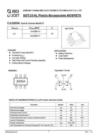
JIANGSU CHANGJING ELECTRONICS TECHNOLOGY CO., LTD SOT-23-6L Plastic-Encapsulate MOSFETS CJL8205A Dual N-Channel MOSFET ID V(BR)DSS RDS(on)MAX SOT-23-6L 30 m @4.5V 5A 20V @2.5V 45m FEATURE APPLICATION TrenchFET Power MOSFET Battery Protection Excellent RDS(on) Load Switch Low Gate Charge Power Management High Power and Current Handing Ca
0.5. Size:2146K htsemi
pt8205a.pdf 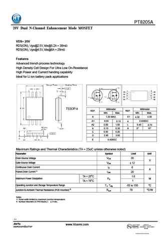
PT8205A 20V Dual N-Channel Enhancement Mode MOSFET VDS= 20V RDS(ON), Vgs@ 2.5V, Ids@ 5.2A = 38m RDS(ON), Vgs@ 4.5V, Ids@ 6A = 28m Features Advanced trench process technology High Density Cell Design For Ultra Low On-Resistance High Power and Current handing capability Ideal for Li ion battery pack applications 1 8 D1 D2 2 7 S1 S2 3 6 S1 S2 4 5 G1 G2 TSSOP-8 Mi
0.6. Size:434K cet
ceg8205a.pdf 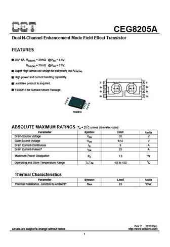
CEG8205A Dual N-Channel Enhancement Mode Field Effect Transistor FEATURES 20V, 6A, RDS(ON) = 25m @VGS = 4.5V. RDS(ON) = 35m @VGS = 2.5V. Super High dense cell design for extremely low RDS(ON). High power and current handing capability. D 1 8 D Lead free product is acquired. 2 7 S2 S1 TSSOP-8 for Surface Mount Package. S1 3 6 S2 4 G1 5 G2 G2 S2 S2 G1 D S1 S1 D TSSOP
0.7. Size:344K gsme
gm8205a.pdf 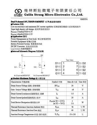
Guilin Strong Micro-Electronics Co.,Ltd. Guilin Strong Micro-Electronics Co.,Ltd. Guilin Strong Micro-Electronics Co.,Ltd. Guilin Strong Micro-Electronics Co.,Ltd. GM8205A Dual N-channel 20V, TSSOP-8 MOSFET N- Dual N-channel 20V, TSSOP-8 MOSFET N- Dual N-channel 20V, TSSOP-8 MOSFET N- Dual N-channel 20V, TSSOP-8 MOSFET N-
0.8. Size:51K hsmc
h8205a.pdf 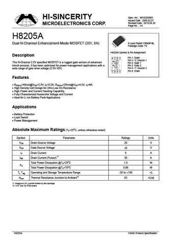
Spec. No. MOS200905 HI-SINCERITY Issued Date 2009.02.27 Revised Date 2010.06.30 MICROELECTRONICS CORP. Page No. 1/4 H8205A 8-Lead Plastic TSSOP-8L Dual N-Channel Enhancement-Mode MOSFET (20V, 6A) Package Code TS H8205A Symbol & Pin Assignment Description 8 7 6 5 Pin 1 Drain Pin 2 / 3 Source 1 Q2 This N-Channel 2.5V specified MOSFET is a rugged gate version
0.9. Size:381K shenzhen
s8205a.pdf 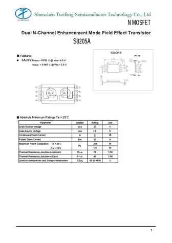
Shenzhen Tuofeng Semiconductor Technology Co., Ltd SMD Type MOSFET N MOSFET Dual N-Channel Enhancement Mode Field Effect Transistor S8205A TSSOP-8 Unit mm Features 5A,20V.rDS(on) = 0.025 @VGS =4.5 V rDS(on) = 0.040 @VGS =2.5 V. Absolute Maximum Ratings Ta = 25 Parameter Symbol Rating Unit Drain-Source Voltage VDS 20 V Gate-Source Voltage VGS 8 V Continuous Drain Current ID A 5
0.10. Size:450K silikron
ssf8205a.pdf 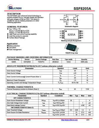
SSF8205A DESCRIPTION D1 D2 The SSF8205A uses advanced trench technology to provide excellent R , low gate charge and operation DS(ON) with gate voltages as low as 0.65V. This device is G1 G2 suitable for use as a Battery protection or in other Switching application. S1 S2 Schematic diagram GENERAL FEATURES V = 20V,I = 6A DS D R
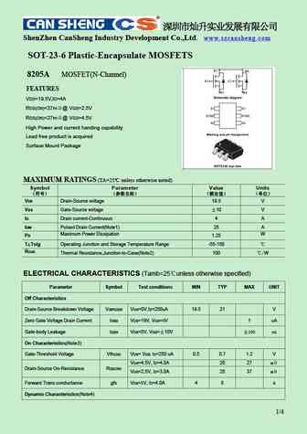
0.11. Size:292K can-sheng
cs8205a 6a sot-23-6.pdf 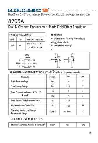
ShenZhen CanSheng Industry Development Co.,Ltd. www.szcansheng.com 8205A Dual N-Channel E nhancement Mode Field E ffect Transistor PR ODUC T S UMMAR Y F E ATUR E S S uper high dense cell design for low R DS (ON). VDS S ID R DS (ON) ( m ) Max R ugged and reliable. 27.5 @ VG S = 4.0V 20V 6A S urface Mount Package. 37.5@V G S = 2.5V D1 D2 -
0.14. Size:235K sino
sm8205ao.pdf 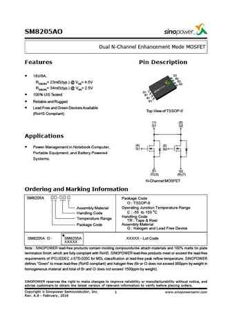
SM8205AO Dual N-Channel Enhancement Mode MOSFET Features Pin Description D2 18V/6A, S2 S2 RDS(ON)= 23m (typ.) @ VGS= 4.5V G2 RDS(ON)= 34m (typ.) @ VGS= 2.5V D1 100% UIS Tested S1 S1 G1 Reliable and Rugged Lead Free and Green Devices Available Top View of TSSOP-8 (RoHS Compliant) (1) (8) D1 D2 Applications (4) (5) Power Management in Notebook Computer, G1 G2 Po
0.15. Size:287K first silicon
ftk8205a.pdf 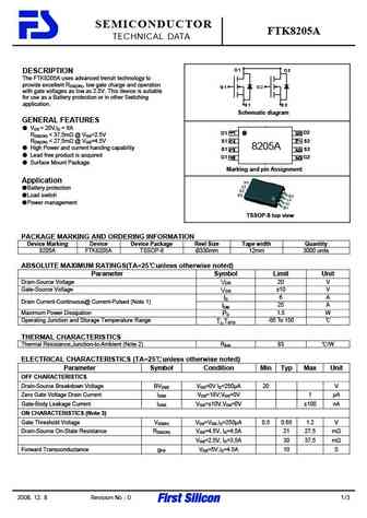
SEMICONDUCTOR FTK8205A TECHNICAL DATA D 1 D 2 DESCRIPTION The FTK8205A uses advanced trench technology to provide excellent RDS(ON), low gate charge and operation G 1 G 2 with gate voltages as low as 2.5V. This device is suitable for use as a Battery protection or in other Switching application. S 1 S 2 Schematic diagram GENERAL FEATURES VDS = 20V,ID = 6A D1 D2 RD
0.16. Size:672K kexin
ki8205a.pdf 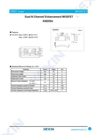
SMD Type MOSFET SMDType Dual N-Channel Enhancement MOSFET KI8205A TSSOP-8 Unit mm Features 6.45+0.1 -0.1 6.5 A, 20 V. rDS(on) = 0.025 @ VGS = 4.5 V 4.45+0.1 -0.1 rDS(on) = 0.029 @ VGS = 2.5 V. Absolute Maximum Ratings Ta = 25 Parameter Symbol Rating Unit Drain-Source Voltage VDS 20 V Gate-Source Voltage VGS 10 V Continuous Drain Current ID 6.5 A Pulsed Drain Current IDM 20 A
0.17. Size:629K belling
blm8205a.pdf 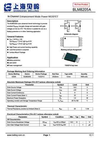
Pb Free Product BLM8205A N-Channel Enhancement Mode Power MOSFET D1 D2 Description The BLM8205A uses advanced trench technology to provide G1 G2 excellent RDS(ON), low gate charge and operation with gate voltages as low as 2.5V. This device is suitable for use as a Battery protection or in other Switching application. S1 S2 Schematic diagram General Features VDS = 19.
0.18. Size:403K ncepower
nce8205a.pdf 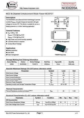
Pb Free Product http //www.ncepower.com NCE8205A NCE N-Channel Enhancement Mode Power MOSFET D1 D2 Description The NCE8205A uses advanced trench technology to provide G1 G2 excellent RDS(ON), low gate charge and operation with gate voltages as low as 2.5V. This device is suitable for use as a Battery protection or in other Switching application. S1 S2 Schematic diagram Gener
0.19. Size:410K prospower
ps8205a.pdf 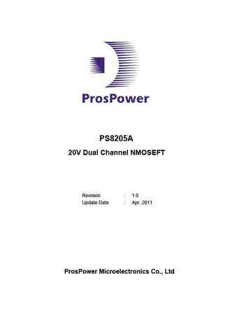
PS8205A 20V Dual Channel NMOSEFT Revision 1.0 Update Date Apr. 2011 ProsPower Microelectronics Co., Ltd PS8205A 20V Dual Channel NMOSFET 2. Applications 1. General Description Battery management in nomadic equipment The PS8205A uses advanced trench technology DC motor control and design to provide excellent Rds(on) with low DC-DC converters gate charge. This
0.20. Size:376K semtron
smc8205aw.pdf 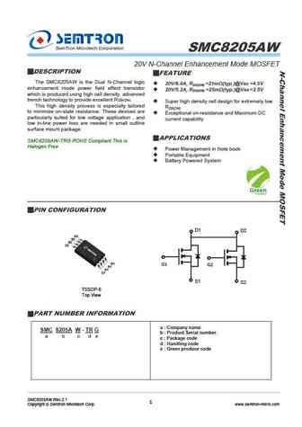
SMC8205AW 20V N-Channel Enhancement Mode MOSFET DESCRIPTION FEATURE The SMC8205AW is the Dual N-Channel logic 20V/6.0A, RDS(ON) =21m (typ.)@VGS =4.5V enhancement mode power field effect transistor 20V/5.2A, RDS(ON) =25m (typ.)@VGS =2.5V which is produced using high cell density. advanced trench technology to provide excellent RDS(ON). Super high density ce
0.21. Size:499K semtron
smc8205as.pdf 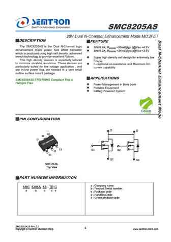
SMC8205AS 20V Dual N-Channel Enhancement Mode MOSFET DESCRIPTION FEATURE The SMC8205AS is the Dual N-Channel logic 20V/6.0A, RDS(ON) =20m (typ.)@VGS =4.5V enhancement mode power field effect transistor 20V/5.2A, RDS(ON) =24m (typ.)@VGS =2.5V which is produced using high cell density. advanced trench technology to provide excellent RDS(ON). Super high densi
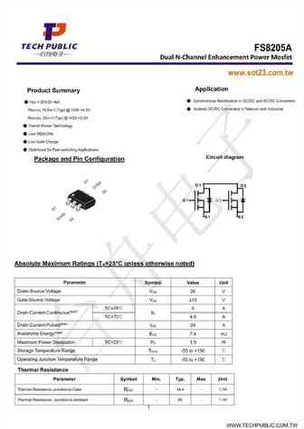
0.23. Size:302K fortune semi
fs8205a.pdf 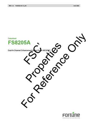
REV. 1.2 FS8205A-DS-12_EN AUG 2009 Datasheet FS8205A Dual N-Channel Enhancement Mode Power MOSFET Only FSC Properties Reference For FS8205A Fortune Semiconductor Corporation 28F., No.27, Sec. 2, Zhongzheng E. Rd., Danshui Town, Taipei County 251, Taiwan Tel. 886-2-28094742 Fax 886-2-28094874 www.ic-fortune.com This manual contai
0.24. Size:4365K fuxinsemi
fs8205a.pdf 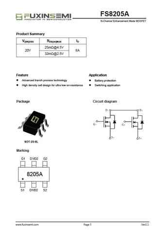
FS8205A N-Channel Enhancement Mode MOSFET Product Summary V(BR)DSS RDS(on)MAX ID 25m @4.5V 20V 6A 32m @2.5V Feature Application Advanced trench process technology Battery protection High density cell design for ultra low on-resistance Switching application Package Circuit diagram SOT-23-6L Marking G1 D1/D2 G2 8205A S1 D1/D2 S2 www.fuxinsemi.com Page 1 Ver2.1 FS
0.25. Size:573K eternal
et8205a.pdf 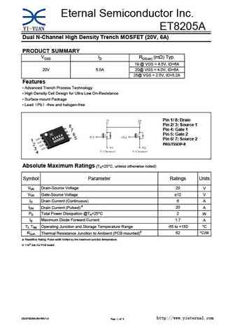
Eternal Semiconductor Inc. ET8205A Dual N-Channel High Density Trench MOSFET (20V, 6A) PRODUCT SUMMARY VDSS ID RDS(on) (m ) Typ. 19 @ VGS = 4.5V, ID=6A 20V 6.0A 20@ VGS = 4.0V, ID=6A 25@ VGS = 2.5V, ID=5.2A Features Advanced Trench Process Technology High Density Cell Design for Ultra Low On-Resistance Surface mount Package Lead Pb -free and halogen-free Pin 1
0.26. Size:451K guangdong hottech
s8205a.pdf 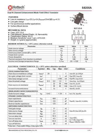
S8205A Dual N-Channel Enhancement Mode Field Effect Transistor FEATURES Low on-resistance V =20V,I =5A,R 25m @V =4.5V DS D DS(ON) GS Low gate charge For synchronous rectifier applications Surface Mount device SOT-23-6 MECHANICAL DATA Case SOT-23-6 Case Material Molded Plastic. UL flammability Classification Rating 94V-0 Moisture Sensitivity L
0.27. Size:986K jiejie micro
jmtm8205a.pdf 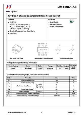
JMTM8205A Description JMT Dual N-channel Enhancement Mode Power MosFET Features Applicatio l 19.5V, 5A l Load Switch RDS(ON)
0.28. Size:2585K cn szxunrui
si8205a.pdf 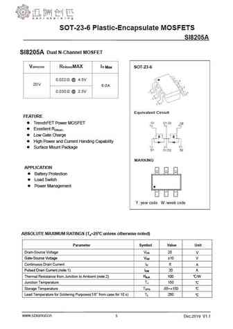
SOT-23-6 Plastic-Encapsulate MOSFETS SI8205A Dual N-Channel MOSFET SI8205A V(BR)DSS RDS(on)MAX ID Max SOT-23-6 0.022 @ 4.5V 20V 6.0A 0.030 @ 2.5V Equivalent Circuit FEATURE TrenchFET Power MOSFET Excellent RDS(on) Low Gate Charge High Power and Current Handing Capability Surface Mount Package MARKING APPLICATION Battery Protection Load Switch
0.29. Size:328K cn shenzhen fuman elec
.8205a.pdf 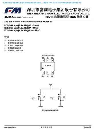
FM , FM WWW.SZLCSC.COM, SHEN ZHEN FINE MADE ELECTRONICS GROUP CO., LTD. .8205A ( S&CIC1850) 20V N MOS 2 3 4 20V N-Channel Enhancement-Mode MOSFET RDS(ON), Vgs@2.5V, Ids@3A = 2
0.30. Size:2391K cn tuofeng
s8205a.pdf 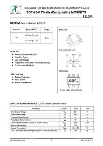
SHENZHEN TUOFENG SEMICONDUCTOR TECHNOLOGY CO.,LTD SOT-23-6 Plastic-Encapsulate MOSFETS S8205A S8205A Dual N-Channel MOSFET V(BR)DSS RDS(on)MAX ID Max SOT-23-6 0.022 @ 4.5V 20V 6.0A 0.030 @ 2.5V Equivalent Circuit FEATURE TrenchFET Power MOSFET Excellent RDS(on) Low Gate Charge High Power and Current Handing Capability Surface Mount Package MARKING APPLI
0.31. Size:1703K winsok
wst8205a.pdf 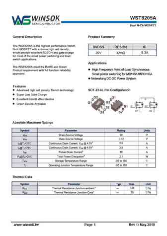
WST8205A Dual N-Ch MOSFET General Description Product Summery The WST8205A is the highest performance trench BVDSS RDSON ID N-ch MOSFET with extreme high cell density , which provide excellent RDSON and gate charge 20V 32m 5.3A for most of the small power switching and load switch applications. Applications The WST8205A meet the RoHS and Green High Frequency Point-of-Load
0.32. Size:422K cn sino-ic
se8205a.pdf 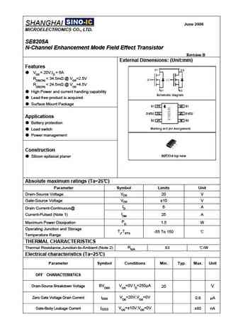
SHANGHAI June 2006 MICROELECTRONICS CO., LTD. SE8205A N-Channel Enhancement Mode Field Effect Transistor Revision B External Dimensions (Unit mm) Features VDS = 20V,ID = 6A RDS(ON)
0.33. Size:787K cn vbsemi
vbzc8205a.pdf 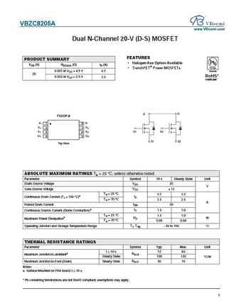
VBZC8205A www.VBsemi.com Dual N-Channel 20-V (D-S) MOSFET FEATURES PRODUCT SUMMARY Halogen-free Option Available VDS (V) RDS(on) ( )ID (A) Pb-free TrenchFET Power MOSFETs 0.025 at VGS = 4.5 V Available 4.5 20 RoHS* 0.032 at VGS = 2.5 V 3.5 COMPLIANT D D TSSOP-8 D D 1 8 S S 1 2 7 2 S S G1 G2 1 3 6 2 G 1 4 G 2 5 S1 S2 Top View ABSOLUTE MAXIMUM RA
0.34. Size:1472K cn vbsemi
ut8205ag-ag6.pdf 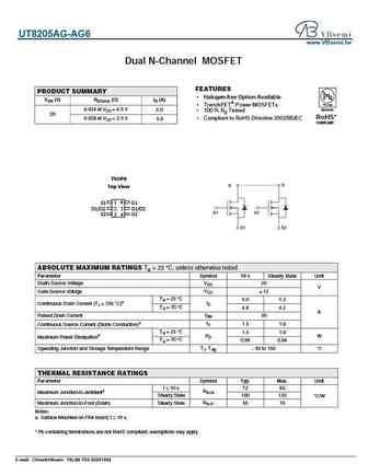
UT8205AG-AG6 www.VBsemi.tw Dual N-Channel MOSFET FEATURES PRODUCT SUMMARY Halogen-free Option Available VDS (V) RDS(on) ( )ID (A) Pb-free TrenchFET Power MOSFETs 0.024 at VGS = 4.5 V Available 6.0 100 % Rg Tested 20 RoHS* 0.028 at VGS = 2.5 V Compliant to RoHS Directive 2002/95/EC 5.0 COMPLIANT TSOP6 D D Top View S1 1 6 G1 D1/D2 2 5 D1/D2 G1 G2 S2 G2
0.35. Size:1138K cn vbsemi
vbzb8205a.pdf 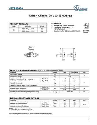
VBZB8205A www.VBsemi.com Dual N-Channel 20-V (D-S) MOSFET FEATURES PRODUCT SUMMARY Halogen-free Option Available VDS (V) RDS(on) ( )ID (A) Pb-free TrenchFET Power MOSFETs 0.024 at VGS = 4.5 V Available 6.0 100 % Rg Tested 20 RoHS* 0.028 at VGS = 2.5 V Compliant to RoHS Directive 2002/95/EC 5.0 COMPLIANT TSOP6 D D Top View S1 1 6 G1 D1/D2 2 5 D1/D2 G1 G
0.36. Size:405K cn tech public
ut8205ag-ag6.pdf 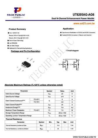
www.sot23.com.tw www.sot23.com.tw www.sot23.com.tw www.sot23.com.tw www.sot23.com.tw www.sot23.com.tw www.sot23.com.tw www.sot23.com.tw www.sot23.com.tw www.sot23.com.tw
0.39. Size:1323K cn yangzhou yangjie elec
yjs8205a.pdf 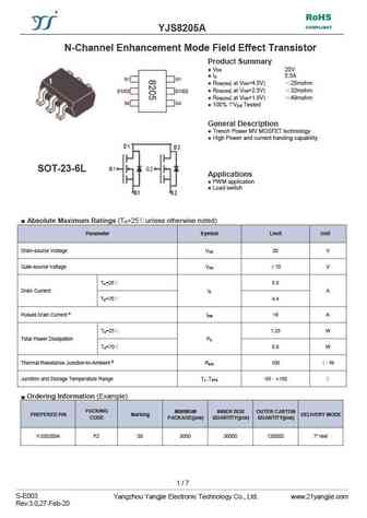
RoHS COMPLIANT YJS8205A N-Channel Enhancement Mode Field Effect Transistor Product Summary V 20V DS I 5.5A D R ( at V =4.5V) 25mohm DS(ON) GS R ( at V =2.5V) 32mohm DS(ON) GS R ( at V =1.8V) 49mohm DS(ON) GS 100% V Tested DS General Description Trench Power MV MOSFET technology High Power and current handing capability
0.40. Size:407K cn wuxi unigroup
ttk8205a.pdf 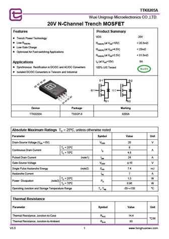
TTK8205A Wuxi Unigroup Microelectronics CO.,LTD. 20V N-Channel Trench MOSFET Features Product Summary VDS 20V Trench Power Technology Low RDS(ON) RDS(ON) (at VGS=10V)
0.41. Size:438K cn hmsemi
hm8205a.pdf 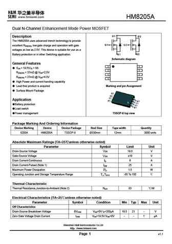
HM8205A Dual N-Channel Enhancement Mode Power MOSFET D1 D2 Description The HM8205A uses advanced trench technology to provide G1 G2 excellent RDS(ON), low gate charge and operation with gate voltages as low as 2.5V. This device is suitable for use as a Battery protection or in other Switching application. S1 S2 Schematic diagram General Features VDS = 19.5V,ID = 6A RDS(
0.42. Size:355K cn haohai electr
h8205a.pdf 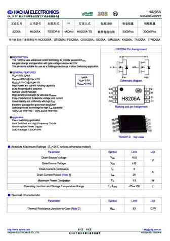
H8205A N-Channel MOSFET 6A, 19.5V, H 8205A H8205A TSSOP-8 HAOHAI H8205A-TS 3000Pcs 30000Pcs NCE8205A UT8205A FS8205A CEG8205A S8205A GM8205A KI8205A TA8205A STN8205A H8205A
0.43. Size:1271K cn apm
ap8205a-21.pdf 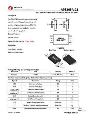
AP8205A-21 20V N+N-Channel Enhancement Mode MOSFET Description The AP8205A-21 uses advanced trench technology to provide excellent R , low gate charge and DS(ON) operation with gate voltages as low as 2.5V. This device is suitable for use as a Battery protection or in other Switching application. General Features V =20V I =6.5A DS D R
Другие IGBT... 50N03, 5P40, 60N04, 6706A, 68P40, 80N03, 80N04, 80N08TR, 75N75, 8205B, G3205, G1010, G3710, 5N20A, 630A, 640, 18N20