640 datasheet, аналоги, основные параметры
Наименование производителя: 640 📄📄
Тип транзистора: MOSFET
Полярность: N
Предельные значения
Pd ⓘ - Максимальная рассеиваемая мощность: 139 W
|Vds|ⓘ - Максимально допустимое напряжение сток-исток: 200 V
|Vgs|ⓘ - Максимально допустимое напряжение затвор-исток: 30 V
|Id| ⓘ - Максимально допустимый постоянный ток стока: 18 A
Tj ⓘ - Максимальная температура канала: 150 °C
Электрические характеристики
tr ⓘ - Время нарастания: 150 ns
Cossⓘ - Выходная емкость: 190 pf
RDSonⓘ - Сопротивление сток-исток открытого транзистора: 0.18 Ohm
Тип корпуса: TO220
📄📄 Копировать
Аналог (замена) для 640
- подборⓘ MOSFET транзистора по параметрам
640 даташит
640.pdf
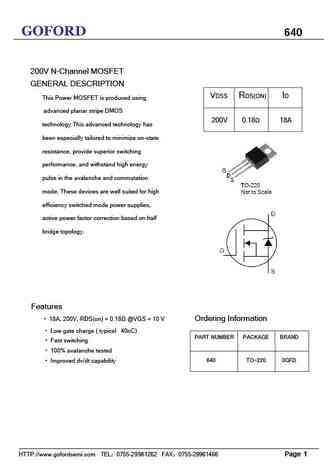
GOFORD 640 200V N-Channel MOSFET GENERAL DESCRIPTION VDSS RDS(ON) ID This Power MOSFET is produced using advanced planar stripe DMOS 200V 0.18 18A technology.This advanced technology has been especially tailored to minimize on-state resistance, provide superior switching performance, and withstand high energy pulse in the avalanche and commutation mode. These devices are well sui
640 f640 i640 e640 b640 d640.pdf
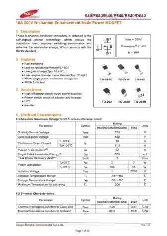
640/F640/I640/E640/B640/D640 18A 200V N-channel Enhancement Mode Power MOSFET 1 Description These N-channel enhanced vdmosfets, is obtained by the 2 D V = 200V self-aligned planar technology which reduce the DSS conduction loss, improve switching performance and R = 0.12 DS(on) (TYP) G enhance the avalanche energy. Which accords with the 1 RoHS standard. I = 18A 3 S D 2 Featur
aon6407.pdf
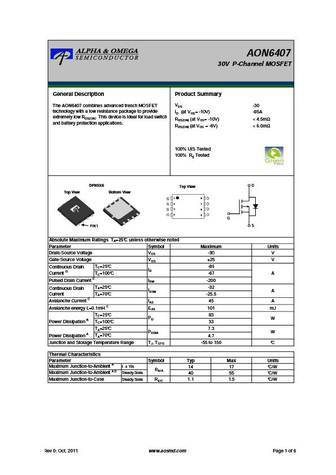
AON6407 30V P-Channel MOSFET General Description Product Summary VDS The AON6407 combines advanced trench MOSFET -30 technology with a low resistance package to provide ID (at VGS= -10V) -85A extremely low RDS(ON). This device is ideal for load switch RDS(ON) (at VGS= -10V)
mmbt3640.pdf
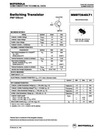
MOTOROLA Order this document SEMICONDUCTOR TECHNICAL DATA by MMBT3640LT1/D Switching Transistor MMBT3640LT1 COLLECTOR PNP Silicon 3 Motorola Preferred Device 1 BASE 2 3 EMITTER MAXIMUM RATINGS 1 Rating Symbol Value Unit 2 Collector Emitter Voltage VCEO 12 Vdc CASE 318 08, STYLE 6 Collector Base Voltage VCBO 12 Vdc SOT 23 (TO 236AB) Emitter Base Voltage V
mrf6402.pdf

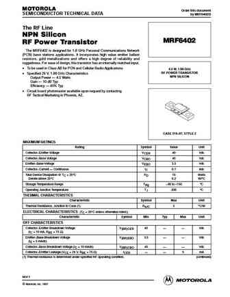
MOTOROLA Order this document SEMICONDUCTOR TECHNICAL DATA by MRF6402/D The RF Line NPN Silicon MRF6402 RF Power Transistor The MRF6402 is designed for 1.8 GHz Personal Communications Network (PCN) base stations applications. It incorporates high value emitter ballast resistors, gold metallizations and offers a high degree of reliability and ruggedness. For ease of design, this transi
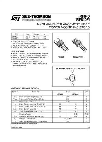
irf640.rev1.pdf
ClibPDF - www.fastio.com ClibPDF - www.fastio.com ClibPDF - www.fastio.com
mrf6402rev7.pdf
MOTOROLA Order this document SEMICONDUCTOR TECHNICAL DATA by MRF6402/D The RF Line NPN Silicon MRF6402 RF Power Transistor The MRF6402 is designed for 1.8 GHz Personal Communications Network (PCN) base stations applications. It incorporates high value emitter ballast resistors, gold metallizations and offers a high degree of reliability and ruggedness. For ease of design, this transi
mrf6404rev2.pdf

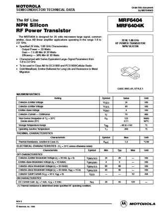
MOTOROLA Order this document SEMICONDUCTOR TECHNICAL DATA by MRF6404/D The RF Line MRF6404 NPN Silicon MRF6404K RF Power Transistor The MRF6404 is designed for 26 volts microwave large signal, common emitter, class AB linear amplifier applications operating in the range 1.8 to 30 W, 1.88 GHz 2.0 GHz. RF POWER TRANSISTOR Specified 26 Volts, 1.88 GHz Characteristics NPN SILICON

mrf6401r.pdf
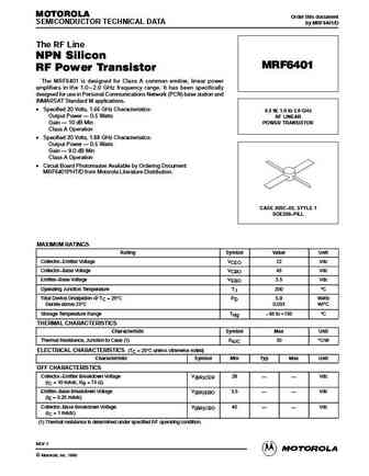
MOTOROLA Order this document SEMICONDUCTOR TECHNICAL DATA by MRF6401/D The RF Line NPN Silicon MRF6401 RF Power Transistor The MRF6401 is designed for Class A common emitter, linear power amplifiers in the 1.0 2.0 GHz frequency range. It has been specifically designed for use in Personal Communications Network (PCN) base station and INMARSAT Standard M applications. Specifie
2n5640.pdf
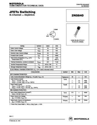
MOTOROLA Order this document SEMICONDUCTOR TECHNICAL DATA by 2N5640/D JFETs Switching N Channel Depletion 2N5640 1 DRAIN 3 1 GATE 2 3 2 SOURCE CASE 29 04, STYLE 5 TO 92 (TO 226AA) Rating Symbol Value Unit Drain Source Voltage VDS 30 Vdc Drain Gate Voltage VDG 30 Vdc Reverse Gate Source Voltage VGSR 30 Vdc Forward Gate Current IGF 10 mAdc Total Device Dissip

mrf6404.pdf

MOTOROLA Order this document SEMICONDUCTOR TECHNICAL DATA by MRF6404/D The RF Line MRF6404 NPN Silicon RF Power Transistor The MRF6404 is designed for 26 volts microwave large signal, common emitter, class AB linear amplifier applications operating in the range 1.8 to 30 W, 1.88 GHz 2.0 GHz. RF POWER TRANSISTOR Specified 26 Volts, 1.88 GHz Characteristics NPN SILICON Output Po
mrf6401p.pdf
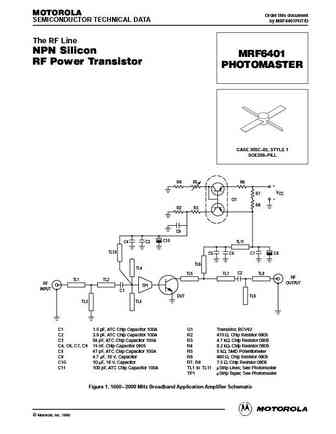
MOTOROLA Order this document SEMICONDUCTOR TECHNICAL DATA by MRF6401PHT/D The RF Line NPN Silicon MRF6401 RF Power Transistor PHOTOMASTER CASE 305C 02, STYLE 1 SOE200 PILL R4 R5 R6 + VCC R7 Q1 R8 R2 R3 C9 C10 C4 C3 TL11 TL10 C5 C6 C7 C8 TL6 TL4 C2 TL5 TL7 TL9 RF TL1 TL2 OUTPUT RF TP1 INPUT C1 DUT TL8 TL3 TL4 C1 1.5 pF, ATC Chip Capacitor 100A Q1 Tran
mps3640r.pdf
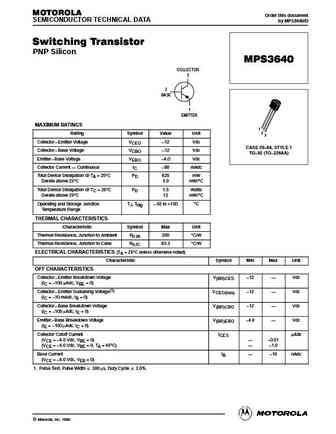
MOTOROLA Order this document SEMICONDUCTOR TECHNICAL DATA by MPS3640/D Switching Transistor PNP Silicon MPS3640 COLLECTOR 3 2 BASE 1 EMITTER MAXIMUM RATINGS 1 2 Rating Symbol Value Unit 3 Collector Emitter Voltage VCEO 12 Vdc CASE 29 04, STYLE 1 Collector Base Voltage VCBO 12 Vdc TO 92 (TO 226AA) Emitter Base Voltage VEBO 4.0 Vdc Collector Current
mrf6404r.pdf
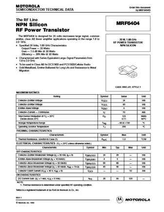
MOTOROLA Order this document SEMICONDUCTOR TECHNICAL DATA by MRF6404/D The RF Line MRF6404 NPN Silicon RF Power Transistor The MRF6404 is designed for 26 volts microwave large signal, common emitter, class AB linear amplifier applications operating in the range 1.8 to 30 W, 1.88 GHz 2.0 GHz. RF POWER TRANSISTOR Specified 26 Volts, 1.88 GHz Characteristics NPN SILICON Output Po
mrf6404 mrf6404k.pdf
MOTOROLA Order this document SEMICONDUCTOR TECHNICAL DATA by MRF6404/D The RF Line MRF6404 NPN Silicon MRF6404K RF Power Transistor The MRF6404 is designed for 26 volts microwave large signal, common emitter, class AB linear amplifier applications operating in the range 1.8 to 30 W, 1.88 GHz 2.0 GHz. RF POWER TRANSISTOR Specified 26 Volts, 1.88 GHz Characteristics NPN SILICON
mrf6409.pdf
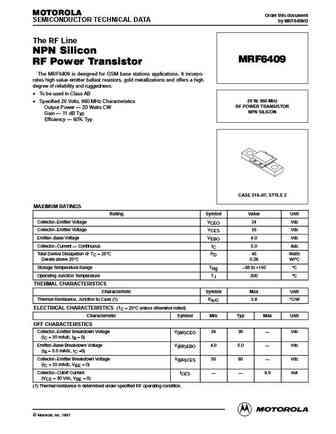
MOTOROLA Order this document SEMICONDUCTOR TECHNICAL DATA by MRF6409/D The RF Line NPN Silicon MRF6409 RF Power Transistor The MRF6409 is designed for GSM base stations applications. It incorpo- rates high value emitter ballast resistors, gold metallizations and offers a high degree of reliability and ruggedness. To be used in Class AB Specified 26 Volts, 960 MHz Characteris
bc636 bc638 bc640.pdf
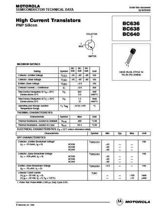
MOTOROLA Order this document SEMICONDUCTOR TECHNICAL DATA by BC636/D High Current Transistors BC636 PNP Silicon BC638 COLLECTOR BC640 2 3 BASE 1 EMITTER 1 MAXIMUM RATINGS 2 3 BC BC BC 636 638 640 Rating Symbol Unit CASE 29 04, STYLE 14 TO 92 (TO 226AA) Collector Emitter Voltage VCEO 45 60 80 Vdc Collector Base Voltage VCBO 45 60 80 Vdc Emitt
mrf6402r.pdf
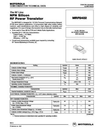
MOTOROLA Order this document SEMICONDUCTOR TECHNICAL DATA by MRF6402/D The RF Line NPN Silicon MRF6402 RF Power Transistor The MRF6402 is designed for 1.8 GHz Personal Communications Network (PCN) base stations applications. It incorporates high value emitter ballast resistors, gold metallizations and offers a high degree of reliability and ruggedness. For ease of design, this transi
mrf6409rev0.pdf

MOTOROLA Order this document SEMICONDUCTOR TECHNICAL DATA by MRF6409/D The RF Line NPN Silicon MRF6409 RF Power Transistor The MRF6409 is designed for GSM base stations applications. It incorpo- rates high value emitter ballast resistors, gold metallizations and offers a high degree of reliability and ruggedness. To be used in Class AB Specified 26 Volts, 960 MHz Characteris
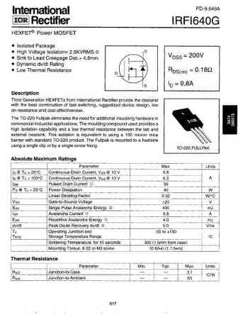
irfi640gpbf.pdf
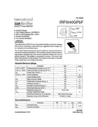
PD- 95420 IRFI640GPbF Lead-Free 06/16/04 Document Number 91150 www.vishay.com 1 IRFI640GPbF Document Number 91150 www.vishay.com 2 IRFI640GPbF Document Number 91150 www.vishay.com 3 IRFI640GPbF Document Number 91150 www.vishay.com 4 IRFI640GPbF Document Number 91150 www.vishay.com 5 IRFI640GPbF Document Number 91150 www.vishay.com 6 IRFI640GPbF Document Num
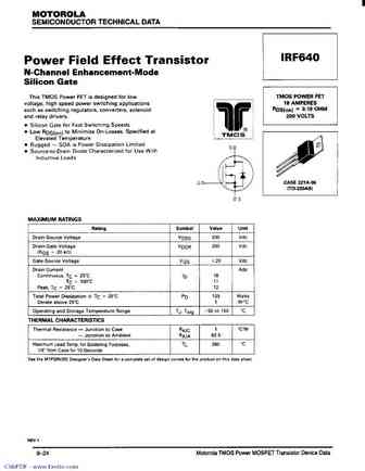
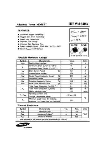
irf640n.pdf
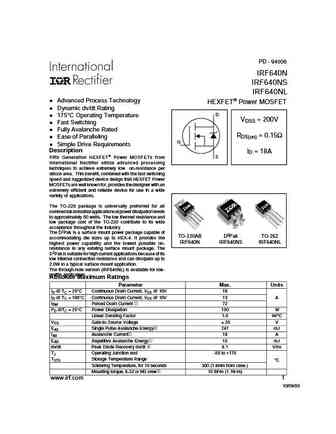
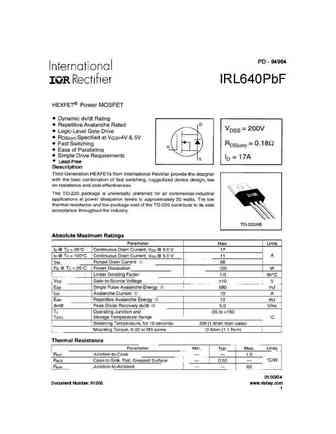
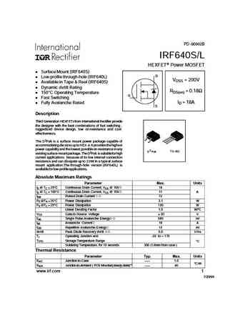
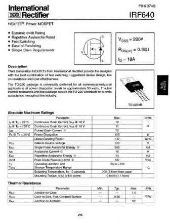
PD - 94006 IRF640N IRF640NS IRF640NL Advanced Process Technology HEXFET Power MOSFET Dynamic dv/dt Rating D 175 C Operating Temperature VDSS = 200V Fast Switching Fully Avalanche Rated RDS(on) = 0.15 Ease of Paralleling G Simple Drive Requirements Description ID = 18A Fifth Generation HEXFET Power MOSFETs from S International Rectifier utilize advanced processi
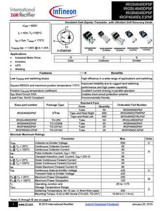
irgb4640d.pdf

IRGS4640DPbF IRGSL4640DPbF IRGB4640DPbF IRGP4640D(-E)PbF Insulated Gate Bipolar Transistor with Ultrafast Soft Recovery Diode VCES = 600V C IC = 40A, TC =100 C E E E E tSC 5 s, TJ(max) = 175 C E G C C C C C G G G G G E IRGP4640D-EPbF VCE(ON) typ. = 1.60V @ IC = 24A IRGS4640DPbF IRGP4640DPbF IRGSL4640DPbF IRGB4640DPbF TO-247AD D2Pak TO-247AC
irlml6401gpbf.pdf
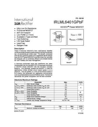
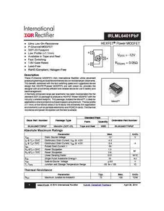
PD - 96160 IRLML6401GPbF HEXFET Power MOSFET l Ultra Low On-Resistance l P-Channel MOSFET l SOT-23 Footprint l Low Profile (
irlml6402gpbf.pdf
PD - 96161A IRLML6402GPbF HEXFET Power MOSFET l Ultra Low On-Resistance l P-Channel MOSFET l SOT-23 Footprint G 1 l Low Profile (
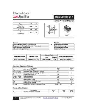
irlml6401.pdf
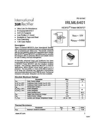
PD- 93756C IRLML6401 HEXFET Power MOSFET Ultra Low On-Resistance P-Channel MOSFET SOT-23 Footprint G 1 Low Profile (
irf640pbf.pdf
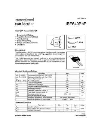
PD - 94930 IRF640PbF Lead-Free 1/8/04 Document Number 91036 www.vishay.com 1 IRF640PbF Document Number 91036 www.vishay.com 2 IRF640PbF Document Number 91036 www.vishay.com 3 IRF640PbF Document Number 91036 www.vishay.com 4 IRF640PbF Document Number 91036 www.vishay.com 5 IRF640PbF Document Number 91036 www.vishay.com 6 IRF640PbF TO-220AB Package Outline D
irf640nlpbf irf640npbf irf640nspbf.pdf

PD - 95046A IRF640NPbF IRF640NSPbF l Advanced Process Technology IRF640NLPbF l Dynamic dv/dt Rating HEXFET Power MOSFET l 175 C Operating Temperature l Fast Switching D VDSS = 200V l Fully Avalanche Rated l Ease of Paralleling l Simple Drive Requirements RDS(on) = 0.15 G l Lead-Free Description ID = 18A Fifth Generation HEXFET Power MOSFETs from S International Rectif
irf640npbf irf640nspbf irf640nlpbf.pdf
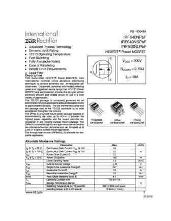
PD - 95046A IRF640NPbF IRF640NSPbF l Advanced Process Technology IRF640NLPbF l Dynamic dv/dt Rating HEXFET Power MOSFET l 175 C Operating Temperature l Fast Switching D VDSS = 200V l Fully Avalanche Rated l Ease of Paralleling l Simple Drive Requirements RDS(on) = 0.15 G l Lead-Free Description ID = 18A Fifth Generation HEXFET Power MOSFETs from S International Rectif
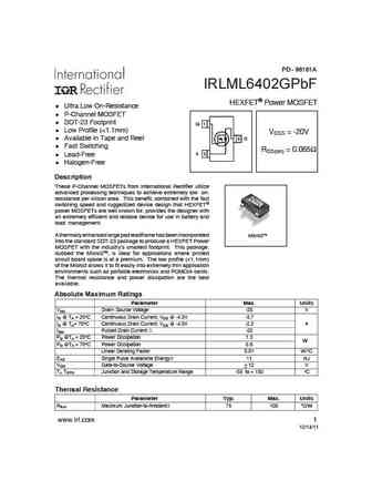
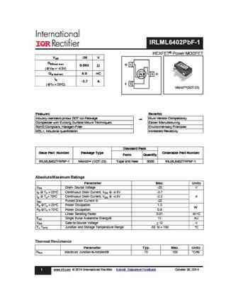
irlml6402.pdf
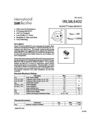
PD- 93755 IRLML6402 HEXFET Power MOSFET Ultra Low On-Resistance D P-Channel MOSFET SOT-23 Footprint VDSS = -20V Low Profile (
irgs4640d.pdf
IRGS4640DPbF IRGSL4640DPbF IRGB4640DPbF IRGP4640D(-E)PbF Insulated Gate Bipolar Transistor with Ultrafast Soft Recovery Diode VCES = 600V C IC = 40A, TC =100 C E E E E tSC 5 s, TJ(max) = 175 C E G C C C C C G G G G G E IRGP4640D-EPbF VCE(ON) typ. = 1.60V @ IC = 24A IRGS4640DPbF IRGP4640DPbF IRGSL4640DPbF IRGB4640DPbF TO-247AD D2Pak TO-247AC
irlml6401pbf-1.pdf
IRLML6401PbF-1 HEXFET Power MOSFET VDS -12 V RDS(on) max G 1 0.05 (@V = -4.5V) GS Qg (typical) 10 nC 3 D ID -4.3 A S 2 (@T = 25 C) A Micro3 Features Benefits Industry-standard pinout SOT-23 Package Multi-Vendor Compatibility Compatible with Existing Surface Mount Techniques Easier Manufacturing RoHS Compliant, Halogen-Free Environmentally Friendlier MSL1, Indu
irlml6402pbf-1.pdf
IRLML6402PbF-1 HEXFET Power MOSFET VDS -20 V RDS(on) max G 1 0.065 (@V = -4.5V) GS Qg (typical) 8.0 nC 3 D ID -3.7 A S 2 (@T = 25 C) A Micro3 (SOT-23) Features Benefits Industry-standard pinout SOT-23 Package Multi-Vendor Compatibility Compatible with Existing Surface Mount Techniques Easier Manufacturing RoHS Compliant, Halogen-Free Environmentally Friendlier
irlml6401pbf.pdf
IRLML6401PbF l Ultra Low On-Resistance HEXFET Power MOSFET l P-Channel MOSFET l SOT-23 Footprint G 1 l Low Profile (
irl640pbf.pdf
PD - 94964 IRL640PbF Lead-Free 01/30/04 Document Number 91305 www.vishay.com 1 IRL640PbF Document Number 91305 www.vishay.com 2 IRL640PbF Document Number 91305 www.vishay.com 3 IRL640PbF Document Number 91305 www.vishay.com 4 IRL640PbF Document Number 91305 www.vishay.com 5 IRL640PbF Document Number 91305 www.vishay.com 6 IRL640PbF Document Number 91305 ww
irli640g.pdf
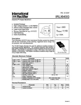
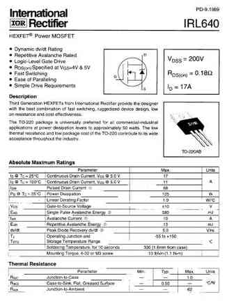
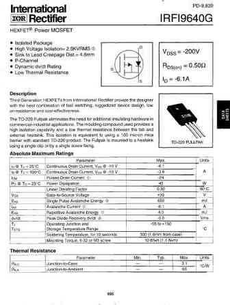
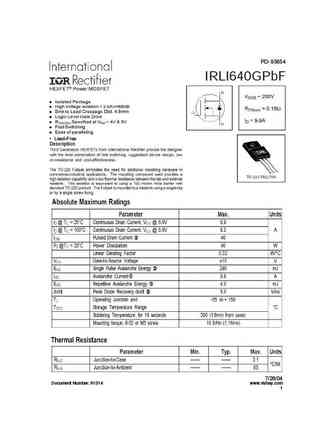
PD - 9.1237 IRLI640G HEXFET Power MOSFET Isolated Package High Voltage Isolation = 2.5KVRMS VDSS = 200V Sink to Lead Creepage Dist. 4.8mm Logic-Level Gate Drive RDS(on) = 0.18 RDS(ON) Specified at VGS = 4V & 5V Fast Switching Ease of paralleling ID = 9.9A Description Third Generation HEXFETs from International Rectifier provide the designer with the best combination of fast
irgsl4640d.pdf

IRGS4640DPbF IRGSL4640DPbF IRGB4640DPbF IRGP4640D(-E)PbF Insulated Gate Bipolar Transistor with Ultrafast Soft Recovery Diode VCES = 600V C IC = 40A, TC =100 C E E E E tSC 5 s, TJ(max) = 175 C E G C C C C C G G G G G E IRGP4640D-EPbF VCE(ON) typ. = 1.60V @ IC = 24A IRGS4640DPbF IRGP4640DPbF IRGSL4640DPbF IRGB4640DPbF TO-247AD D2Pak TO-247AC
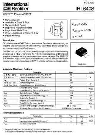
irf640s.pdf
PD -90902B IRF640S/L HEXFET Power MOSFET Surface Mount (IRF640S) D Low-profile through-hole (IRF640L) VDSS = 200V Available in Tape & Reel (IRF640S) Dynamic dv/dt Rating RDS(on) = 0.18 150 C Operating Temperature G Fast Switching ID = 18A Fully Avalanche Rated S Description Third Generation HEXFETs from International Rectifier provide the designer with the best co
irli640gpbf.pdf
PD- 95654 IRLI640GPbF Lead-Free 7/26/04 Document Number 91314 www.vishay.com 1 IRLI640GPbF Document Number 91314 www.vishay.com 2 IRLI640GPbF Document Number 91314 www.vishay.com 3 IRLI640GPbF Document Number 91314 www.vishay.com 4 IRLI640GPbF Document Number 91314 www.vishay.com 5 IRLI640GPbF Document Number 91314 www.vishay.com 6 IRLI640GPbF Peak Diode Re
irl640spbf.pdf
PD- 95585 IRL640SPbF Lead-Free 07/20/04 Document Number 91306 www.vishay.com 1 IRL640SPbF Document Number 91306 www.vishay.com 2 IRL640SPbF Document Number 91306 www.vishay.com 3 IRL640SPbF Document Number 91306 www.vishay.com 4 IRL640SPbF Document Number 91306 www.vishay.com 5 IRL640SPbF Document Number 91306 www.vishay.com 6 IRL640SPbF Peak Diode Recovery
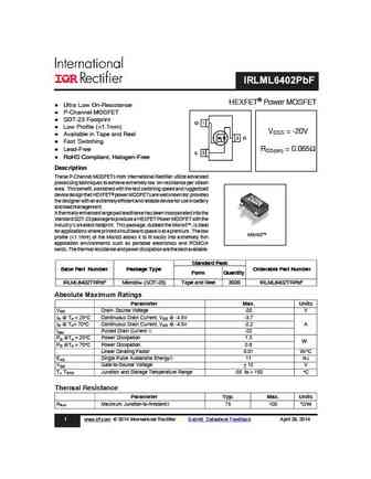
irf640s-l.pdf
PD - 95113 IRF640S/LPbF Lead-Free 3/16/04 Document Number 91037 www.vishay.com 1 IRF640S/LPbF Document Number 91037 www.vishay.com 2 IRF640S/LPbF Document Number 91037 www.vishay.com 3 IRF640S/LPbF Document Number 91037 www.vishay.com 4 IRF640S/LPbF Document Number 91037 www.vishay.com 5 IRF640S/LPbF Document Number 91037 www.vishay.com 6 IRF640S/LPbF Docum
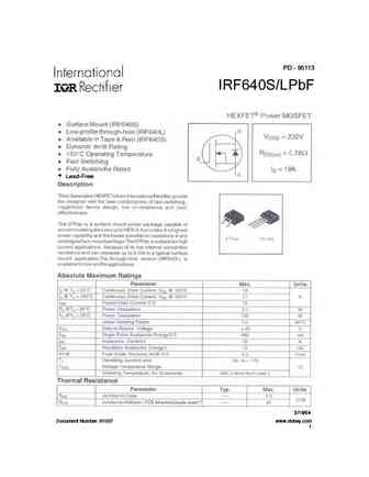
auirf7640s2tr.pdf
PD -97551 AUIRF7640S2TR AUTOMOTIVE GRADE AUIRF7640S2TR1 DirectFET Power MOSFET Advanced Process Technology Optimized for Class D Audio Amplifier and High Speed V(BR)DSS 60V Switching Applications RDS(on) typ. 27m Low Rds(on) for Improved Efficiency max. 36m Low Qg for Better THD and Improved Efficiency Low Qrr for Better THD and Lower EMI RG (typical)
irgp4640d.pdf

IRGS4640DPbF IRGSL4640DPbF IRGB4640DPbF IRGP4640D(-E)PbF Insulated Gate Bipolar Transistor with Ultrafast Soft Recovery Diode VCES = 600V C IC = 40A, TC =100 C E E E E tSC 5 s, TJ(max) = 175 C E G C C C C C G G G G G E IRGP4640D-EPbF VCE(ON) typ. = 1.60V @ IC = 24A IRGS4640DPbF IRGP4640DPbF IRGSL4640DPbF IRGB4640DPbF TO-247AD D2Pak TO-247AC
irlml6402pbf.pdf
IRLML6402PbF HEXFET Power MOSFET l Ultra Low On-Resistance l P-Channel MOSFET l SOT-23 Footprint G 1 l Low Profile (
irfi9640gpbf.pdf
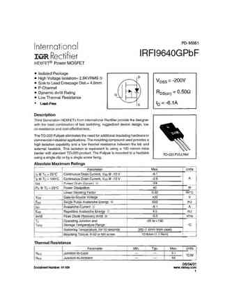
PD- 95351 IRFI9640GPbF Lead-Free 06/04/01 Document Number 91169 www.vishay.com 1 IRFI9640GPbF Document Number 91169 www.vishay.com 2 IRFI9640GPbF Document Number 91169 www.vishay.com 3 IRFI9640GPbF Document Number 91169 www.vishay.com 4 IRFI9640GPbF Document Number 91169 www.vishay.com 5 IRFI9640GPbF Document Number 91169 www.vishay.com 6 IRFI9640GPbF Docum
irf9640spbf.pdf
PD - 95117A IRF9640SPbF Lead-Free 06/09/05 Document Number 91087 www.vishay.com 1 IRF9640SPbF Document Number 91087 www.vishay.com 2 IRF9640SPbF Document Number 91087 www.vishay.com 3 IRF9640SPbF Document Number 91087 www.vishay.com 4 IRF9640SPbF Document Number 91087 www.vishay.com 5 IRF9640SPbF Document Number 91087 www.vishay.com 6 IRF9640SPbF Peak Diode
irf9640pbf.pdf
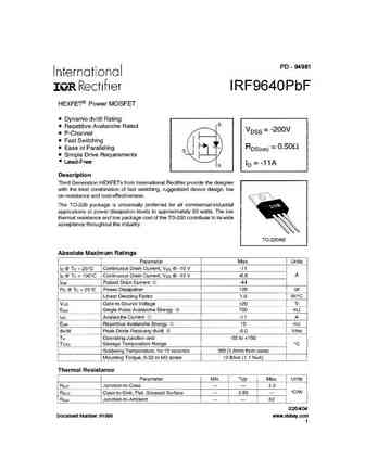
PD - 94981 IRF9640PbF Lead-Free 02/04/04 Document Number 91086 www.vishay.com 1 IRF9640PbF Document Number 91086 www.vishay.com 2 IRF9640PbF Document Number 91086 www.vishay.com 3 IRF9640PbF Document Number 91086 www.vishay.com 4 IRF9640PbF Document Number 91086 www.vishay.com 5 IRF9640PbF Document Number 91086 www.vishay.com 6 IRF9640PbF TO-220AB Package O
irgp4640.pdf
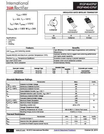
IRGP4640PbF IRGP4640-EPbF INSULATED GATE BIPOLAR TRANSISTOR VCES = 600V C C C IC = 40A, TC = 100 C tSC 5 s, TJ(max) = 175 C G E E C C G E G VCE(on) typ. = 1.60V @ IC = 24A n-channel TO-247AC TO-247AD IRGP4640PbF IRGP4640-EP GC E Applications Gate Collector Emitter Inverters UPS Welding Features Benefits High efficiency in a wide range of applications
buk9540 buk9640-100a 2.pdf
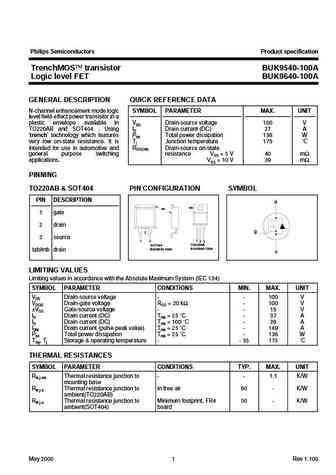
Philips Semiconductors Product specification TrenchMOS transistor BUK9540-100A Logic level FET BUK9640-100A GENERAL DESCRIPTION QUICK REFERENCE DATA N-channel enhancement mode logic SYMBOL PARAMETER MAX. UNIT level field-effect power transistor in a plastic envelope available in VDS Drain-source voltage 100 V TO220AB and SOT404 . Using ID Drain current (DC) 37 A trench techn
irf640 s 1.pdf
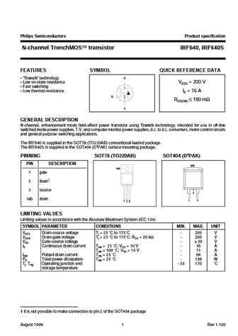
Philips Semiconductors Product specification N-channel TrenchMOS transistor IRF640, IRF640S FEATURES SYMBOL QUICK REFERENCE DATA Trench technology d Low on-state resistance VDSS = 200 V Fast switching Low thermal resistance ID = 16 A g RDS(ON) 180 m s GENERAL DESCRIPTION N-channel, enhancement mode field-effect power transistor using Trench technolog
pmbt3640 cnv 2.pdf
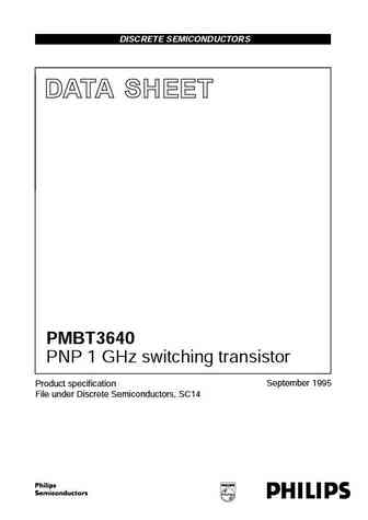
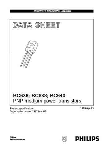
DISCRETE SEMICONDUCTORS DATA SHEET PMBT3640 PNP 1 GHz switching transistor September 1995 Product specification File under Discrete Semiconductors, SC14 Philips Semiconductors Product specification PNP 1 GHz switching transistor PMBT3640 DESCRIPTION PINNING PNP general purpose switching PIN DESCRIPTION fpage 3 transistor in a SOT23 package. Code V25 1 base 2 emitter 12 3 col
bc640 bcp53 bcx53.pdf
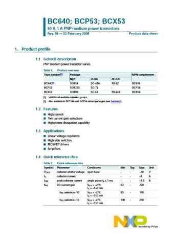
BC640; BCP53; BCX53 80 V, 1 A PNP medium power transistors Rev. 08 22 February 2008 Product data sheet 1. Product profile 1.1 General description PNP medium power transistor series. Table 1. Product overview Type number[1] Package NPN complement NXP JEITA JEDEC BC640[2] SOT54 SC-43A TO-92 BC639 BCP53 SOT223 SC-73 - BCP56 BCX53 SOT89 SC-62 TO-243 BCX56 [1] Valid for all available
buk7640-100a 1.pdf
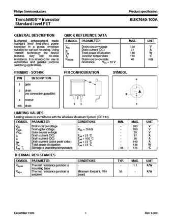
Philips Semiconductors Product specification TrenchMOS transistor BUK7640-100A Standard level FET GENERAL DESCRIPTION QUICK REFERENCE DATA N-channel enhancement mode SYMBOL PARAMETER MAX. UNIT standard level field-effect power transistor in a plastic envelope VDS Drain-source voltage 100 V suitable for surface mounting. Using ID Drain current (DC) 37 A trench technology the d
bc636 bc638 bc640 3.pdf
DISCRETE SEMICONDUCTORS DATA SHEET book, halfpage M3D186 BC636; BC638; BC640 PNP medium power transistors 1999 Apr 23 Product specification Supersedes data of 1997 Mar 07 Philips Semiconductors Product specification PNP medium power transistors BC636; BC638; BC640 FEATURES PINNING High current (max. 1 A) PIN DESCRIPTION Low voltage (max. 80 V). 1 base 2 collector APPLI
irf640 irf640fp.pdf
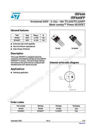
IRF640 IRF640FP N-channel 200V - 0.15 - 18A TO-220/TO-220FP Mesh overlay Power MOSFET General features Type VDSS RDS(on) ID IRF640 200V
irf640f fp.pdf
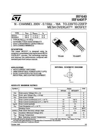
IRF640 IRF640FP N - CHANNEL 200V - 0.150 - 18A TO-220/TO-220FP MESH OVERLAY MOSFET TYPE VDSS RDS(on) ID IRF640 200 V
irf640fp.pdf

IRF640 IRF640FP N-channel 200V - 0.15 - 18A TO-220/TO-220FP Mesh overlay Power MOSFET General features Type VDSS RDS(on) ID IRF640 200V
irf640.pdf
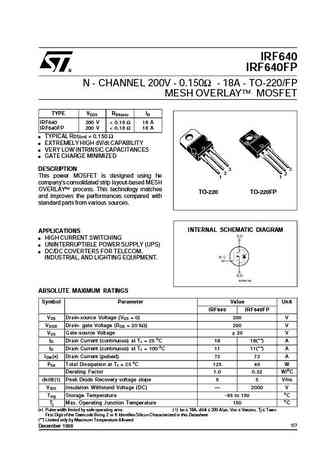
IRF640 IRF640FP N - CHANNEL 200V - 0.150 - 18A - TO-220/FP MESH OVERLAY MOSFET TYPE VDSS RDS(on) ID IRF640 200 V
3stf1640.pdf
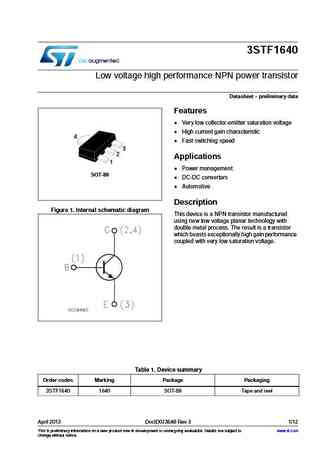
3STF1640 Low voltage high performance NPN power transistor Datasheet - preliminary data Features Very low collector-emitter saturation voltage High current gain characteristic 4 Fast switching speed 3 2 Applications 1 Power management SOT-89 DC-DC converters Automotive Description Figure 1. Internal schematic diagram This device is a NPN transistor manu
mp6404.pdf
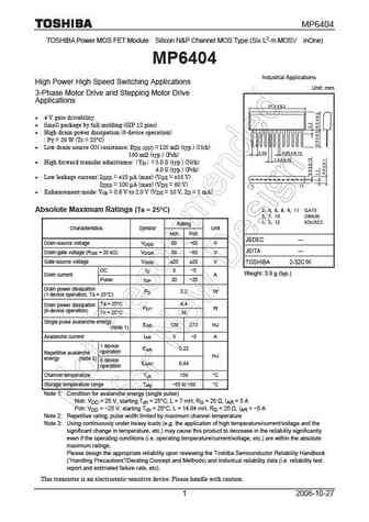
MP6404 TOSHIBA Power MOS FET Module Silicon N&P Channel MOS Type (Six L2- -MOSV inOne) MP6404 Industrial Applications High Power High Speed Switching Applications Unit mm 3-Phase Motor Drive and Stepping Motor Drive Applications 4-V gate drivability Small package by full molding (SIP 12 pins) High drain power dissipation (6-device operation) PT = 36 W (Tc =
tph6400enh.pdf
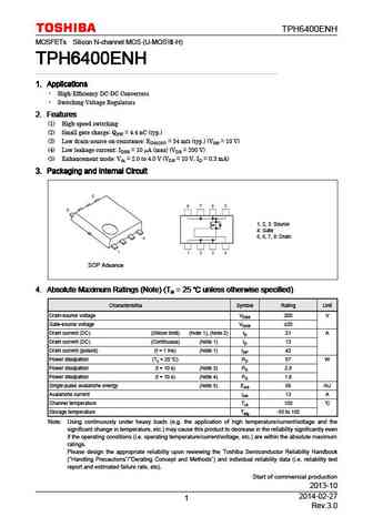
TPH6400ENH MOSFETs Silicon N-channel MOS (U-MOS -H) TPH6400ENH TPH6400ENH TPH6400ENH TPH6400ENH 1. Applications 1. Applications 1. Applications 1. Applications High-Efficiency DC-DC Converters Switching Voltage Regulators 2. Features 2. Features 2. Features 2. Features (1) High-speed switching (2) Small gate charge QSW = 4.4 nC (typ.) (3) Low drain-source on-resista
mch6402.pdf
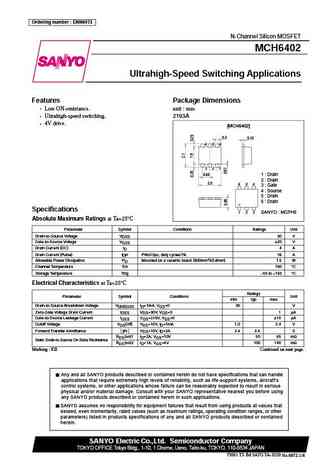
Ordering number ENN6972 MCH6402 N-Channel Silicon MOSFET MCH6402 Ultrahigh-Speed Switching Applications Preliminary Features Package Dimensions Low ON-resistance. unit mm Ultrahigh-speed switching. 2193A 4V drive. [MCH6402] 0.3 0.15 4 5 6 3 2 1 0.65 1 Drain 2 Drain 2.0 6 5 4 3 Gate 4 Source 5 Drain 6 Drain Specifications 1 2 3 SANYO MCPH6
cph6402.pdf
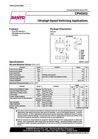
Ordering number EN5983 N-Channel MOS Silicon FET CPH6402 Ultrahigh-Speed Switching Applications Features Package Dimensions Low ON resistance. unit mm Ultrahigh-speed switching. 2151 4V drive. [CPH6402] 0.15 2.9 6 5 4 0 to 0.1 1 Drain 1 2 3 2 Drain 0.95 3 Gate 4 Source 5 Drain 6 Drain 0.4 SANYO CPH6 Specifications Absolute Maximum Ratings at T
cph6401.pdf
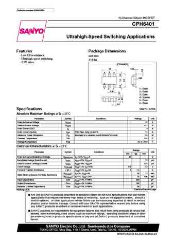
Ordering number ENN6152A N-Channel Silicon MOSFET CPH6401 Ultrahigh-Speed Switching Applications Features Package Dimensions Low ON-resistance. unit mm Ultrahigh-speed switching. 2151A 2.5V drive. [CPH6401] 0.15 2.9 6 5 4 0.05 1 2 3 1 Drain 0.95 2 Drain 3 Gate 4 Source 5 Drain 6 Drain 0.4 SANYO CPH6 Specifications Absolute Maximum Ratings at T
cph6404.pdf
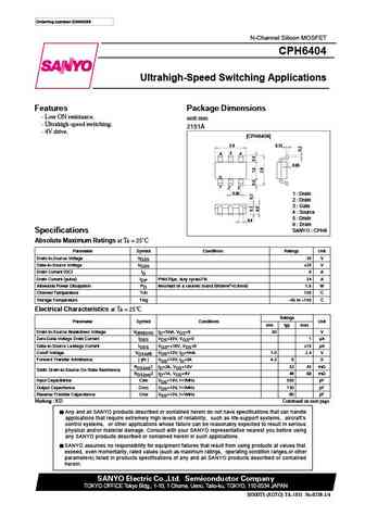
Ordering number ENN6338 N-Channel Silicon MOSFET CPH6404 Ultrahigh-Speed Switching Applications Features Package Dimensions Low ON resistance. unit mm Ultrahigh-speed switching. 2151A 4V drive. [CPH6404] 0.15 2.9 6 5 4 0.05 1 2 3 0.95 1 Drain 2 Drain 3 Gate 4 Source 5 Drain 0.4 6 Drain SANYO CPH6 Specifications Absolute Maximum Ratings at Ta =
mch6401.pdf
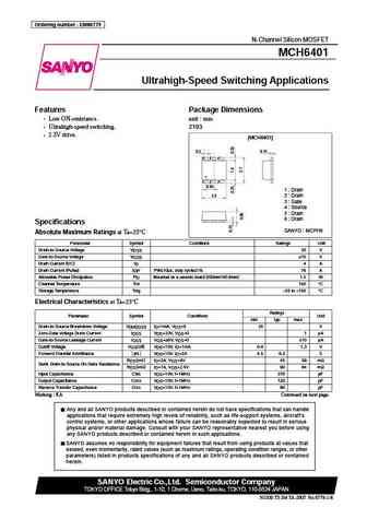
Ordering number ENN6779 MCH6401 N-Channel Silicon MOSFET MCH6401 Ultrahigh-Speed Switching Applications Features Package Dimensions Low ON-resistance. unit mm Ultrahigh-speed switching. 2193 2.5V drive. [MCH6401] 0.3 0.15 6 5 4 1 2 3 0.65 1 Drain 2.0 2 Drain 3 Gate 4 Source 5 Drain 6 Drain Specifications SANYO MCPH6 Absolute Maximum Ratings at
mch6403.pdf
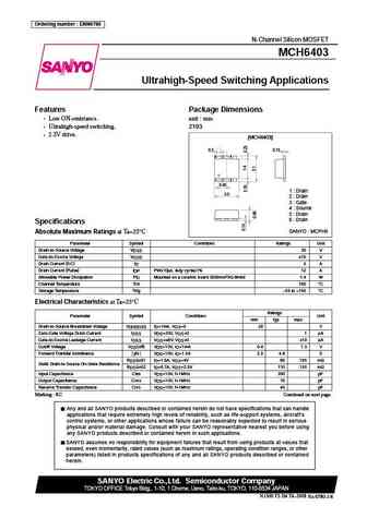
Ordering number ENN6780 MCH6403 N-Channel Silicon MOSFET MCH6403 Ultrahigh-Speed Switching Applications Features Package Dimensions Low ON-resistance. unit mm Ultrahigh-speed switching. 2193 2.5V drive. [MCH6403] 0.3 0.15 6 5 4 1 2 3 0.65 1 Drain 2.0 2 Drain 3 Gate 4 Source 5 Drain 6 Drain Specifications Absolute Maximum Ratings at Ta=25 C SANY
mch6405.pdf
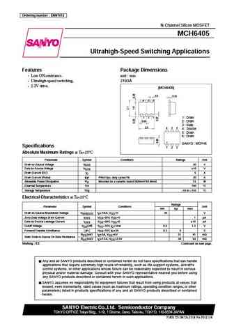
Ordering number ENN7012 MCH6405 N-Channel Silicon MOSFET MCH6405 Ultrahigh-Speed Switching Applications Features Package Dimensions Low ON-resistance. unit mm Ultrahigh-speed switching. 2193A 2.5V drive. [MCH6405] 0.3 0.15 4 5 6 3 2 1 1 Drain 0.65 2 Drain 3 Gate 2.0 6 5 4 4 Source 5 Drain 6 Drain SANYO MCPH6 Specifications 1 2 3 Absolute Ma
cph6403.pdf
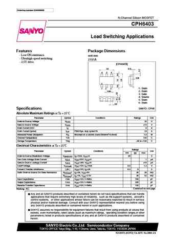
Ordering number ENN5990B N-Channel Silicon MOSFET CPH6403 Load Switching Applications Features Package Dimensions Low ON-resistance. unit mm Ultrahigh-speed switching. 2151A 2.5V drive. [CPH6403] 0.15 2.9 6 5 4 0.05 1 2 3 1 Drain 0.95 2 Drain 3 Gate 4 Source 5 Drain 6 Drain 0.4 SANYO CPH6 Specifications Absolute Maximum Ratings at Ta = 25 C P
cph6406.pdf
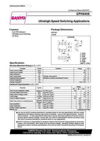
Ordering number ENN6418 N-Channel Silicon MOSFET CPH6406 Ultrahigh-Speed Switching Applications Features Package Dimensions Low ON resistance. unit mm Ultrahigh-speed switching. 2151A 4V drive. [CPH6406] 0.15 2.9 5 6 4 0.05 1 2 3 0.95 1 Drain 2 Drain 3 Gate 4 Source 5 Drain 0.4 6 Drain Specifications SANYO CPH6 Absolute Maximum Ratings at Ta =
rej03g1640 rjk0331dpbds.pdf
To our customers, Old Company Name in Catalogs and Other Documents On April 1st, 2010, NEC Electronics Corporation merged with Renesas Technology Corporation, and Renesas Electronics Corporation took over all the business of both companies. Therefore, although the old company name remains in this document, it is a valid Renesas Electronics document. We appreciate your understanding.
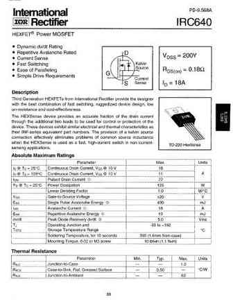
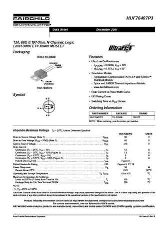
hufa76409p3.pdf
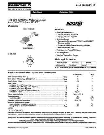
HUFA76409P3 Data Sheet December 2001 17A, 60V, 0.070 Ohm, N-Channel, Logic Level UltraFET Power MOSFET Packaging JEDEC TO-220AB Features Ultra Low On-Resistance SOURCE DRAIN - rDS(ON) = 0.062 , VGS = 10V GATE - rDS(ON) = 0.070 , VGS = 5V Simulation Models - Temperature Compensated PSPICE and SABER Electrical Models DRAIN - Spice and SABER Thermal Impedance
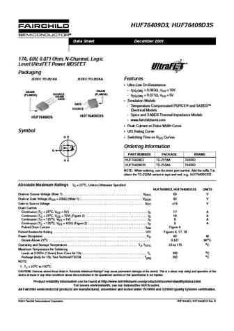
hufa76409d3st.pdf
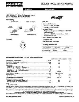
HUFA76409D3, HUFA76409D3ST Data Sheet December 2001 17A, 60V, 0.071 Ohm, N-Channel, Logic Level UltraFET Power MOSFETs Packaging JEDEC TO-251AA JEDEC TO-252AA Features Ultra Low On-Resistance - rDS(ON) = 0.063 , VGS = 10V DRAIN DRAIN SOURCE (FLANGE) (FLANGE) - rDS(ON) = 0.071 , VGS = 5V DRAIN GATE Simulation Models GATE - Temperature Compensated PSPICE and SABER
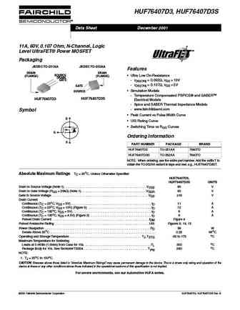
hufa76407d3st hufa76407d3 hufa76407d3s.pdf
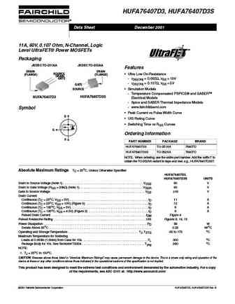
HUFA76407D3, HUFA76407D3S Data Sheet December 2001 11A, 60V, 0.107 Ohm, N-Channel, Logic Level UltraFET Power MOSFETs Packaging JEDEC TO-251AA JEDEC TO-252AA Features DRAIN DRAIN SOURCE Ultra Low On-Resistance (FLANGE) (FLANGE) DRAIN GATE - rDS(ON) = 0.092 , VGS = 10V - rDS(ON) = 0.107 , VGS = 5V GATE SOURCE Simulation Models - Temperature Compensated PSPICE a
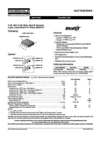
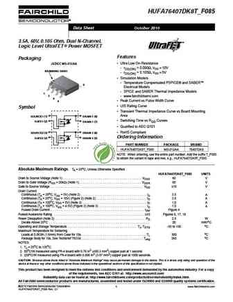
hufa76407dk8t f085.pdf

HUFA76407DK8T_F085 Data Sheet October 2010 3.5A, 60V, 0.105 Ohm, Dual N-Channel, Logic Level UltraFET Power MOSFET Features Packaging JEDEC MS-012AA Ultra Low On-Resistance - rDS(ON) = 0.090 , VGS = 10V BRANDING DASH - rDS(ON) = 0.105 , VGS = 5V Simulation Models - Temperature Compensated PSPICE and SABER 5 Electrical Models - SPICE and SABER Thermal Impedance
huf76407d3st.pdf
HUF76407D3, HUF76407D3S Data Sheet December 2001 11A, 60V, 0.107 Ohm, N-Channel, Logic Level UltraFET Power MOSFET Packaging JEDEC TO-251AA JEDEC TO-252AA Features DRAIN DRAIN SOURCE Ultra Low On-Resistance (FLANGE) (FLANGE) DRAIN GATE - rDS(ON) = 0.092 , VGS = 10V - rDS(ON) = 0.107 , VGS = 5V GATE Simulation Models SOURCE - Temperature Compensated PSPICE and
huf76409d3-s.pdf
HUF76409D3, HUF76409D3S Data Sheet December 2001 17A, 60V, 0.071 Ohm, N-Channel, Logic Level UltraFET Power MOSFET Packaging JEDEC TO-251AA JEDEC TO-252AA Features Ultra Low On-Resistance - rDS(ON) = 0.063 , VGS = 10V DRAIN DRAIN SOURCE (FLANGE) (FLANGE) - rDS(ON) = 0.071 , VGS = 5V DRAIN GATE Simulation Models GATE - Temperature Compensated PSPICE and SABER
huf76407dk8.pdf
HUF76407DK8 Data Sheet December 2001 3.5A, 60V, 0.105 Ohm, Dual N-Channel, Logic Level UltraFET Power MOSFET Packaging Features JEDEC MS-012AA Ultra Low On-Resistance BRANDING DASH - rDS(ON) = 0.090 , VGS = 10V - rDS(ON) = 0.105 , VGS = 5V Simulation Models 5 - Temperature Compensated PSPICE and SABER Electrical Models 1 2 - SPICE and SABER Thermal Impedanc
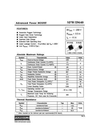
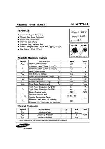
sfw9640tm.pdf

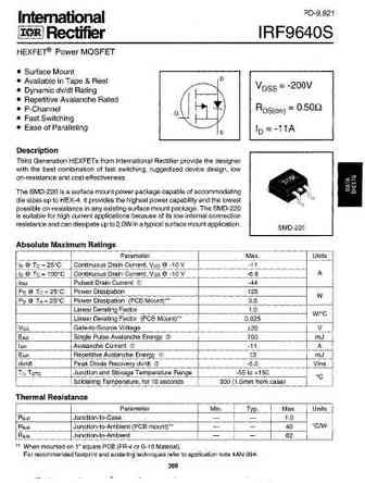
SFW/I9640 Advanced Power MOSFET FEATURES BVDSS = -200 V Avalanche Rugged Technology RDS(on) = 0.5 Rugged Gate Oxide Technology Lower Input Capacitance ID = -11 A Improved Gate Charge Extended Safe Operating Area D2-PAK I2-PAK Lower Leakage Current 10 A (Max.) @ VDS = -200V 2 Low RDS(ON) 0.344 (Typ.) 1 1 2 3 3 1. Gate 2. Drain 3. Source Absolute Maximum
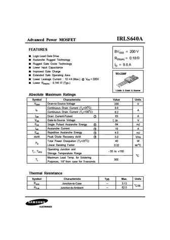
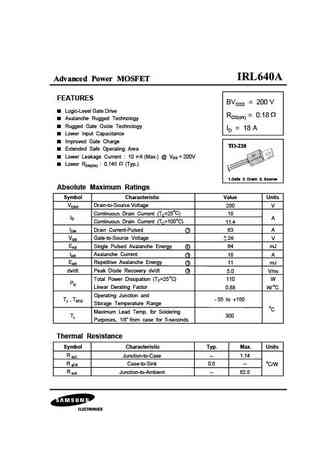
irls640a.pdf
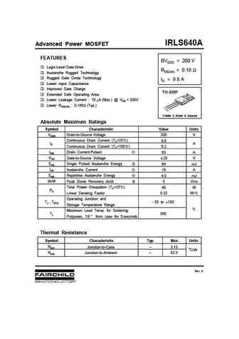
IRLS640A Advanced Power MOSFET FEATURES BVDSS = 200 V Logic-Level Gate Drive RDS(on) = 0.18 Avalanche Rugged Technology Rugged Gate Oxide Technology ID = 9.8 A Lower Input Capacitance Improved Gate Charge TO-220F Extended Safe Operating Area Lower Leakage Current 10 A (Max.) @ VDS = 200V Lower RDS(ON) 0.145 (Typ.) 1 2 3 1.Gate 2. Drain 3. Source Absolute M
sfp9640l.pdf
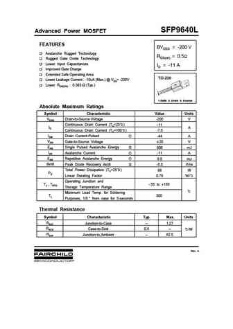
SFP9640L Advanced Power MOSFET FEATURES BVDSS = -200 V Avalanche Rugged Technology RDS(on) = 0.5 Rugged Gate Oxide Technology Lower Input Capacitances ID = -11 A Improved Gate Charge Extended Safe Operating Area TO-220 Lower Leakage Current -10uA (Max.) @ VDS= -200V Lower RDS(ON) 0.383 (Typ.) 1 2 3 1.Gate 2. Drain 3. Source Absolute Maxim
hufa76407p3.pdf

HUFA76407P3 Data Sheet December 2001 12A, 60V, 0.107 Ohm, N-Channel, Logic Level UltraFET Power MOSFET Packaging JEDEC TO-220AB Features Ultra Low On-Resistance SOURCE DRAIN - rDS(ON) = 0.092 , VGS = 10V GATE - rDS(ON) = 0.107 , VGS = 5V Simulation Models - Temperature Compensated PSPICE and SABER Electrical Models DRAIN - Spice and SABER Thermal Impedance M
fdc6401n.pdf
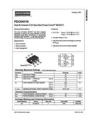
October 2001 FDC6401N Dual N-Channel 2.5V Specified PowerTrench MOSFET General Description Features This Dual N-Channel MOSFET has been designed 3.0 A, 20 V. RDS(ON) = 70 m @ VGS = 4.5 V specifically to improve the overall efficiency of DC/DC RDS(ON) = 95 m @ VGS = 2.5 V converters using either synchronous or conventional switching PWM controllers. It has been optimiz
fdc640p f095.pdf
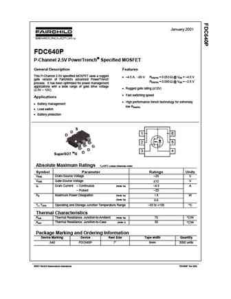
January 2001 FDC640P P-Channel 2.5V PowerTrench Specified MOSFET General Description Features This P-Channel 2.5V specified MOSFET uses a rugged 4.5 A, 20 V RDS(ON) = 0.053 @ VGS = 4.5 V gate version of Fairchild s advanced PowerTrench RDS(ON) = 0.080 @ VGS = 2.5 V process. It has been optimized for power management applications with a wide r
hufa76409d3.pdf

HUFA76409D3, HUFA76409D3ST Data Sheet December 2001 17A, 60V, 0.071 Ohm, N-Channel, Logic Level UltraFET Power MOSFETs Packaging JEDEC TO-251AA JEDEC TO-252AA Features Ultra Low On-Resistance - rDS(ON) = 0.063 , VGS = 10V DRAIN DRAIN SOURCE (FLANGE) (FLANGE) - rDS(ON) = 0.071 , VGS = 5V DRAIN GATE Simulation Models GATE - Temperature Compensated PSPICE and SABER
sfi9640 sfw9640.pdf
SFW/I9640 Advanced Power MOSFET FEATURES BVDSS = -200 V Avalanche Rugged Technology RDS(on) = 0.5 Rugged Gate Oxide Technology Lower Input Capacitance ID = -11 A Improved Gate Charge Extended Safe Operating Area D2-PAK I2-PAK Lower Leakage Current 10 A (Max.) @ VDS = -200V 2 Low RDS(ON) 0.344 (Typ.) 1 1 2 3 3 1. Gate 2. Drain 3. Source Absolute Maximum
fdc640p.pdf

January 2001 FDC640P P-Channel 2.5V PowerTrench Specified MOSFET General Description Features This P-Channel 2.5V specified MOSFET uses a rugged 4.5 A, 20 V RDS(ON) = 0.053 @ VGS = 4.5 V gate version of Fairchild s advanced PowerTrench RDS(ON) = 0.080 @ VGS = 2.5 V process. It has been optimized for power management applications with a wide r
bc636 bc638 bc640.pdf
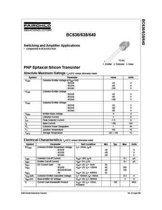
BC636/638/640 Switching and Amplifier Applications Complement to BC635/637/639 TO-92 1 1. Emitter 2. Collector 3. Base PNP Epitaxial Silicon Transistor Absolute Maximum Ratings Ta=25 C unless otherwise noted Symbol Parameter Value Units VCER Collector-Emitter Voltage at RBE=1K BC636 -45 V BC638 -60 V BC640 -100 V VCES Collector-Emitter Voltage BC636 -45 V BC6
huf76407p3.pdf
HUF76407P3 Data Sheet December 2001 12A, 60V, 0.107 Ohm, N-Channel, Logic Level UltraFET Power MOSFET Packaging JEDEC TO-220AB Features Ultra Low On-Resistance SOURCE DRAIN - rDS(ON) = 0.092 , VGS = 10V GATE - rDS(ON) = 0.107 , VGS = 5V Simulation Models - Temperature Compensated PSPICE and SABER Electrical Models DRAIN - Spice and SABER Thermal Impedance Mo
huf76407dk f085.pdf
HUFA76407DK8T_F085 Data Sheet October 2010 3.5A, 60V, 0.105 Ohm, Dual N-Channel, Logic Level UltraFET Power MOSFET Features Packaging JEDEC MS-012AA Ultra Low On-Resistance - rDS(ON) = 0.090 , VGS = 10V BRANDING DASH - rDS(ON) = 0.105 , VGS = 5V Simulation Models - Temperature Compensated PSPICE and SABER 5 Electrical Models - SPICE and SABER Thermal Impedance
irf9640 rf1s9640sm.pdf
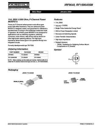
IRF9640, RF1S9640SM Data Sheet January 2002 11A, 200V, 0.500 Ohm, P-Channel Power Features MOSFETs 11A, 200V These are P-Channel enhancement mode silicon-gate rDS(ON) = 0.500 power field-effect transistors. They are advanced power Single Pulse Avalanche Energy Rated MOSFETs designed, tested, and guaranteed to withstand a specified level of energy in the breakdown ava
irl640a.pdf
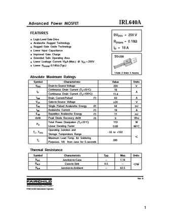
IRL640A FEATURES BVDSS = 200 V Logic-Level Gate Drive RDS(on) = 0.18 Avalanche Rugged Technology Rugged Gate Oxide Technology ID = 18 A Lower Input Capacitance Improved Gate Charge TO-220 Extended Safe Operating Area Lower Leakage Current 10 A (Max.) @ VDS = 200V Lower RDS(ON) 0.145 (Typ.) 1 2 3 1.Gate 2. Drain 3. Source Absolute Maxim
huf76407d3 huf76407d3s.pdf

HUF76407D3, HUF76407D3S Data Sheet December 2001 11A, 60V, 0.107 Ohm, N-Channel, Logic Level UltraFET Power MOSFET Packaging JEDEC TO-251AA JEDEC TO-252AA Features DRAIN DRAIN SOURCE Ultra Low On-Resistance (FLANGE) (FLANGE) DRAIN GATE - rDS(ON) = 0.092 , VGS = 10V - rDS(ON) = 0.107 , VGS = 5V GATE Simulation Models SOURCE - Temperature Compensated PSPICE and
bc640.pdf
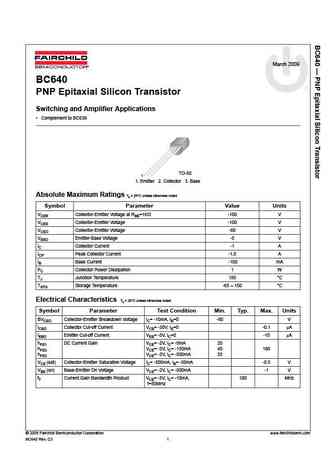
March 2009 BC640 PNP Epitaxial Silicon Transistor Switching and Amplifier Applications Complement to BC639 TO-92 1 1. Emitter 2. Collector 3. Base Absolute Maximum Ratings Ta = 25 C unless otherwise noted Symbol Parameter Value Units VCER Collector-Emitter Voltage at RBE=1K -100 V VCES Collector-Emitter Voltage -100 V VCEO Collector-Emitter Voltage -80 V VEBO Emitter-Base Vo
pn3640 mmbt3640.pdf

PN3640 MMBT3640 C E TO-92 C B B SOT-23 E Mark 2J PNP Switching Transistor This device is designed for very high speed saturated switching at collector currents to 100 mA. Sourced from Process 65. See PN4258 for characteristics. Absolute Maximum Ratings* TA = 25 C unless otherwise noted Symbol Parameter Value Units VCEO Collector-Emitter Voltage 12 V VCBO Collector-Base Voltage
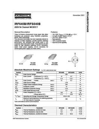
irf640 rf1s640 rf1s640sm.pdf
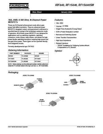
IRF640, RF1S640, RF1S640SM Data Sheet January 2002 18A, 200V, 0.180 Ohm, N-Channel Power Features MOSFETs 18A, 200V These are N-Channel enhancement mode silicon gate rDS(ON) = 0.180 power field effect transistors. They are advanced power Single Pulse Avalanche Energy Rated MOSFETs designed, tested, and guaranteed to withstand a specified level of energy in the breakd
hufa76407dk8t.pdf
HUFA76407DK8 Data Sheet December 2001 3.5A, 60V, 0.105 Ohm, Dual N-Channel, Logic Level UltraFET Power MOSFET Packaging Features JEDEC MS-012AA Ultra Low On-Resistance BRANDING DASH - rDS(ON) = 0.090 , VGS = 10V - rDS(ON) = 0.105 , VGS = 5V Simulation Models 5 - Temperature Compensated PSPICE and SABER Electrical Models 1 2 - SPICE and SABER Thermal Impedan
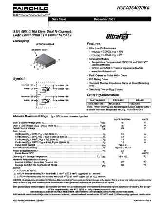
buk9640-100a.pdf
BUK9640-100A N-channel TrenchMOS logic level FET 13 March 2014 Product data sheet 1. General description Logic level N-channel enhancement mode Field-Effect Transistor (FET) in a plastic package using TrenchMOS technology. This product has been designed and qualified to the appropriate AEC standard for use in automotive critical applications. 2. Features and benefits Low conduction
bc640 bcp53 bcx53.pdf

BC640; BCP53; BCX53 80 V, 1 A PNP medium power transistors Rev. 08 22 February 2008 Product data sheet 1. Product profile 1.1 General description PNP medium power transistor series. Table 1. Product overview Type number[1] Package NPN complement NXP JEITA JEDEC BC640[2] SOT54 SC-43A TO-92 BC639 BCP53 SOT223 SC-73 - BCP56 BCX53 SOT89 SC-62 TO-243 BCX56 [1] Valid for all available
buk7640-100a.pdf
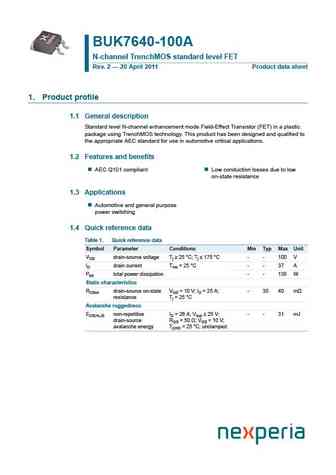
BUK7640-100A N-channel TrenchMOS standard level FET Rev. 2 20 April 2011 Product data sheet 1. Product profile 1.1 General description Standard level N-channel enhancement mode Field-Effect Transistor (FET) in a plastic package using TrenchMOS technology. This product has been designed and qualified to the appropriate AEC standard for use in automotive critical applications. 1.2 F
irlw640a.pdf
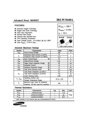
Advanced Power MOSFET FEATURES BVDSS = 200 V Avalanche Rugged Technology RDS(on) = 0.18 Rugged Gate Oxide Technology Lower Input Capacitance ID = 18 A Improved Gate Charge Extended Safe Operating Area 175 Operating Temperature 2 Lower Leakage Current 10 A (Max.) @ VDS = 200V Lower RDS(ON) 0.145 (Typ.) 1 1 2 3 3 1. Gate 2. Drain 3. Source Absolut
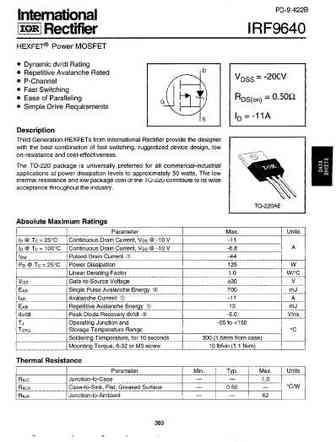
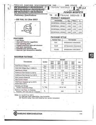
irf9240 irf9241 irf9242 irf9243 irfp9240 irfp9241 irfp9242 irfp9243 irf9640 irf9641 irf9642 irf9643.pdf
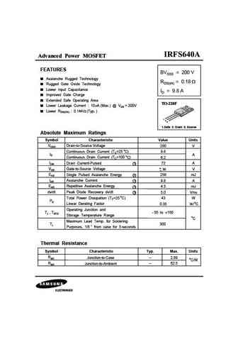
irf640a.pdf
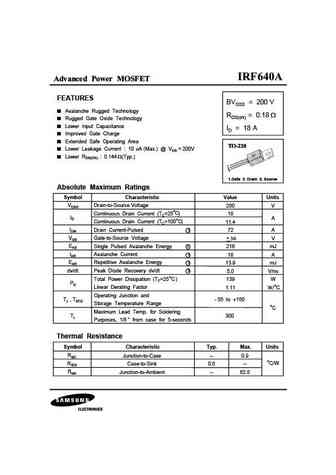
Advanced Power MOSFET FEATURES BVDSS = 200 V Avalanche Rugged Technology RDS(on) = 0.18 Rugged Gate Oxide Technology Lower Input Capacitance ID = 18 A Improved Gate Charge Extended Safe Operating Area Lower Leakage Current 10 A (Max.) @ VDS = 200V Lower RDS(ON) 0.144 (Typ.) 1 2 3 1.Gate 2. Drain 3. Source Absolute Maximum Ratings Symbol Characteristic Val
irls640a.pdf
Advanced Power MOSFET FEATURES BVDSS = 200 V Logic Level Gate Drive RDS(on) = 0.18 Avalanche Rugged Technology Rugged Gate Oxide Technology ID = 9.8 A Lower Input Capacitance Improved Gate Charge Extended Safe Operating Area Lower Leakage Current 10 A (Max.) @ VDS = 200V Lower RDS(ON) 0.145 (Typ.) 1 2 3 1.Gate 2. Drain 3. Source Absolute Maximum Rati
sfs9640.pdf
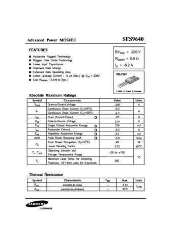
Advanced Power MOSFET FEATURES BVDSS = -200 V Avalanche Rugged Technology RDS(on) = 0.5 Rugged Gate Oxide Technology Lower Input Capacitance ID = -6.2 A Improved Gate Charge Extended Safe Operating Area Lower Leakage Current 10 A (Max.) @ VDS = -200V Low RDS(ON) 0.344 (Typ.) 1 2 3 1.Gate 2. Drain 3. Source Absolute Maximum Ratings Symbol Characteristic V
sfw9640.pdf
Advanced Power MOSFET FEATURES BVDSS = -200 V Avalanche Rugged Technology RDS(on) = 0.5 Rugged Gate Oxide Technology Lower Input Capacitance ID = -11 A Improved Gate Charge Extended Safe Operating Area Lower Leakage Current 10 A (Max.) @ VDS = -200V 2 Low RDS(ON) 0.344 (Typ.) 1 1 2 3 3 1. Gate 2. Drain 3. Source Absolute Maximum Ratings Symbol Cha
sfp9640.pdf

Advanced Power MOSFET FEATURES BVDSS = -200 V Avalanche Rugged Technology RDS(on) = 0.5 Rugged Gate Oxide Technology Lower Input Capacitance ID = -11 A Improved Gate Charge Extended Safe Operating Area Lower Leakage Current -10 A (Max.) @ VDS = -200V Low RDS(ON) 0.344 (Typ.) 1 2 3 1.Gate 2. Drain 3. Source Absolute Maximum Ratings Symbol Characteristic V
irfs640a.pdf
Advanced Power MOSFET FEATURES BVDSS = 200 V Avalanche Rugged Technology RDS(on) = 0.18 Rugged Gate Oxide Technology Lower Input Capacitance ID = 9.8 A Improved Gate Charge Extended Safe Operating Area Lower Leakage Current 10 A (Max.) @ VDS = 200V Lower RDS(ON) 0.144 (Typ. ) 1 2 3 1.Gate 2. Drain 3. Source Absolute Maximum Ratings Symbol Characteristic
bc636 bc638 bc640.pdf
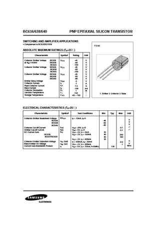
BC636/638/640 PNP EPITAXIAL SILICON TRANSISTOR SWITCHING AND AMPLIFIER APPLICATIONS Complement to BC635/637/639 TO-92 ABSOLUTE MAXIMUM RATINGS (T =25 ) A Characteristic Symbol Rating Unit Collector Emitter Voltage BC636 VCER -45 V at RBE=1Kohm BC638 -60 V BC640 -100 V Collector Emitter Voltage BC636 VCES -45 V BC638 -60 V BC640 -100 V Collector Emitter Voltage BC636 VCE
irl640a.pdf
Advanced Power MOSFET FEATURES BVDSS = 200 V Logic-Level Gate Drive RDS(on) = 0.18 Avalanche Rugged Technology Rugged Gate Oxide Technology ID = 18 A Lower Input Capacitance Improved Gate Charge Extended Safe Operating Area Lower Leakage Current 10 A (Max.) @ VDS = 200V Lower RDS(ON) 0.145 (Typ.) 1 2 3 1.Gate 2. Drain 3. Source Absolute Maximum Ratin
irfw640a.pdf
Advanced Power MOSFET FEATURES BVDSS = 200 V Avalanche Rugged Technology RDS(on) = 0.18 Rugged Gate Oxide Technology Lower Input Capacitance ID = 18 A Improved Gate Charge Extended Safe Operating Area Lower Leakage Current 10 A (Max.) @ VDS = 200V 2 Lower RDS(ON) 0.144 (Typ.) 1 1 2 3 3 1. Gate 2. Drain 3. Source Absolute Maximum Ratings Symbol Cha
bts640s2.pdf
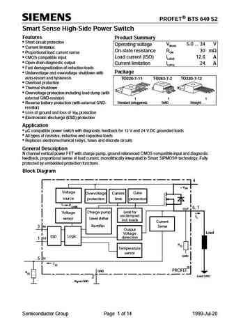
PROFET BTS 640 S2 Smart Sense High-Side Power Switch Features Product Summary Short circuit protection Vbb(on) 5.0 ... 34 V Operating voltage Current limitation On-state resistance RON 30 m Proportional load current sense CMOS compatible input Load current (ISO) IL(ISO) 12.6 A Open drain diagnostic output Current limitation IL(SCr) 24 A Fast demagneti

irfi9640gpbf sihfi9640g.pdf
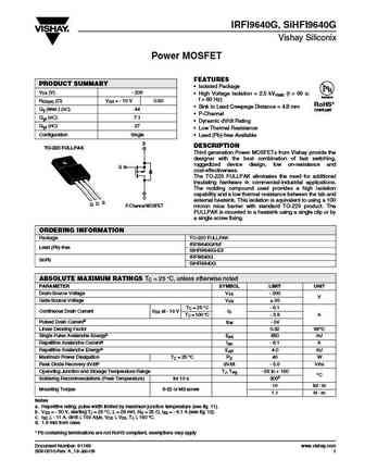
IRFI9640G, SiHFI9640G Vishay Siliconix Power MOSFET FEATURES PRODUCT SUMMARY Isolated Package VDS (V) - 200 High Voltage Isolation = 2.5 kVRMS (t = 60 s; Available f = 60 Hz) RDS(on) ( )VGS = - 10 V 0.50 RoHS* Sink to Lead Creepage Distance = 4.8 mm Qg (Max.) (nC) 44 COMPLIANT P-Channel Qgs (nC) 7.1 Dynamic dV/dt Rating Qgd (nC) 27 Low Thermal Resist
irf9640pbf sihf9640.pdf
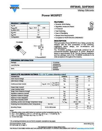
IRF9640, SiHF9640 Vishay Siliconix Power MOSFET FEATURES PRODUCT SUMMARY Dynamic dV/dt Rating VDS (V) - 200 Available Repetitive Avalanche Rated RDS(on) ( )VGS = - 10 V 0.50 RoHS* P-Channel COMPLIANT Qg (Max.) (nC) 44 Fast Switching Qgs (nC) 7.1 Ease of Paralleling Qgd (nC) 27 Simple Drive Requirements Configuration Single Compliant to RoHS Direc
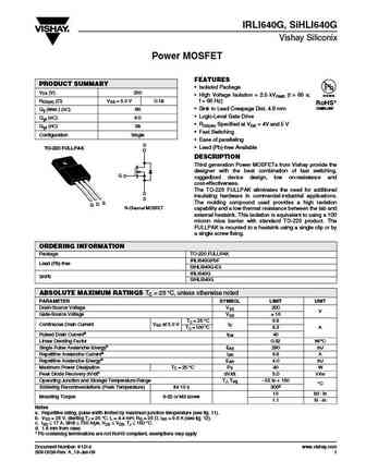
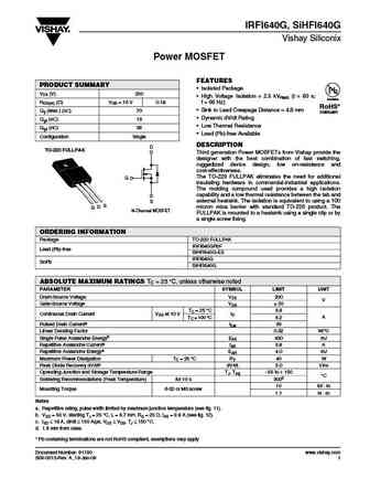
irl640pbf sihl640.pdf

IRL640, SiHL640 Vishay Siliconix Power MOSFET FEATURES PRODUCT SUMMARY Dynamic dV/dt Rating VDS (V) 200 Available Repetitive Avalanche Rated RDS(on) ( )VGS = 5.0 V 0.18 RoHS* Logic-Level Gate Drive COMPLIANT Qg (Max.) (nC) 66 RDS(on) Specified at VGS = 4 V and 5 V Qgs (nC) 9.0 Fast Switching Qgd (nC) 38 Ease of Paralleling Configuration Single Si
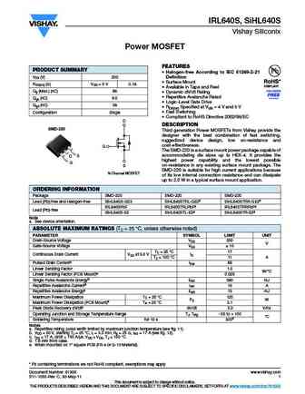
irf640lpbf irf640spbf sihf640l sihf640s.pdf
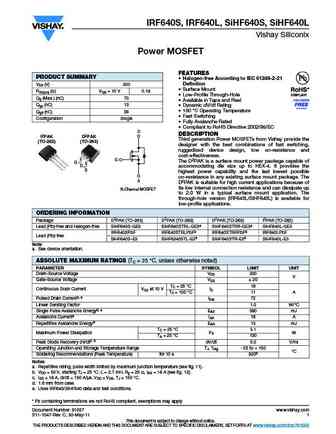
IRF640S, IRF640L, SiHF640S, SiHF640L Vishay Siliconix Power MOSFET FEATURES PRODUCT SUMMARY Halogen-free According to IEC 61249-2-21 Definition VDS (V) 200 Surface Mount RDS(on) ( )VGS = 10 V 0.18 Low-Profile Through-Hole Qg (Max.) (nC) 70 Available in Tape and Reel Qgs (nC) 13 Dynamic dV/dt Rating 150 C Operating Temperature Qgd (nC) 39 Fast Swi
irfi9640g sihfi9640g.pdf

IRFI9640G, SiHFI9640G Vishay Siliconix Power MOSFET FEATURES PRODUCT SUMMARY Isolated Package VDS (V) - 200 High Voltage Isolation = 2.5 kVRMS (t = 60 s; Available f = 60 Hz) RDS(on) ( )VGS = - 10 V 0.50 RoHS* Sink to Lead Creepage Distance = 4.8 mm Qg (Max.) (nC) 44 COMPLIANT P-Channel Qgs (nC) 7.1 Dynamic dV/dt Rating Qgd (nC) 27 Low Thermal Resist
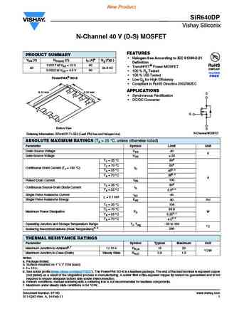
sir640adp.pdf
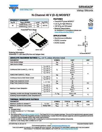
SiR640ADP www.vishay.com Vishay Siliconix N-Channel 40 V (D-S) MOSFET FEATURES PRODUCT SUMMARY TrenchFET power MOSFET VDS (V) RDS(on) ( ) MAX. ID (A) a Qg (TYP.) Low Qg for high efficiency 0.0020 at VGS = 10 V 100 40 28.5 nC 100 % Rg and UIS tested 0.0025 at VGS = 4.5 V 100 Material categorization PowerPAK SO-8 Single for definitions of compliance please se
irl640s sihl640s.pdf
IRL640S, SiHL640S Vishay Siliconix Power MOSFET FEATURES PRODUCT SUMMARY Halogen-free According to IEC 61249-2-21 VDS (V) 200 Definition Surface Mount RDS(on) ( )VGS = 5 V 0.18 Available in Tape and Reel Qg (Max.) (nC) 66 Dynamic dV/dt Rating Repetitive Avalanche Rated Qgs (nC) 9.0 Logic-Level Gate Drive Qgd (nC) 38 RDS(on) Specified at VGS = 4 V a
irl640 sihl640.pdf
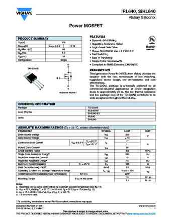
IRL640, SiHL640 Vishay Siliconix Power MOSFET FEATURES PRODUCT SUMMARY Dynamic dV/dt Rating VDS (V) 200 Available Repetitive Avalanche Rated RDS(on) ( )VGS = 5.0 V 0.18 RoHS* Logic-Level Gate Drive COMPLIANT Qg (Max.) (nC) 66 RDS(on) Specified at VGS = 4 V and 5 V Qgs (nC) 9.0 Fast Switching Qgd (nC) 38 Ease of Paralleling Configuration Single Si
sir640dp.pdf
New Product SiR640DP Vishay Siliconix N-Channel 40 V (D-S) MOSFET FEATURES PRODUCT SUMMARY Halogen-free According to IEC 61249-2-21 VDS (V) RDS(on) ( )ID (A)a Qg (Typ.) Definition 0.0017 at VGS = 10 V 60 TrenchFET Power MOSFET 40 34.6 nC 0.0022 at VGS = 4.5 V 60 100 % Rg Tested 100 % UIS Tested PowerPAK SO-8 Low Qg for High Efficiency Compli

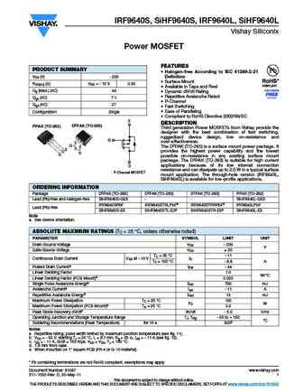
sihfi640g.pdf

IRFI640G, SiHFI640G Vishay Siliconix Power MOSFET FEATURES PRODUCT SUMMARY Isolated Package VDS (V) 200 High Voltage Isolation = 2.5 kVRMS (t = 60 s; Available RDS(on) ( )VGS = 10 V 0.18 f = 60 Hz) RoHS* Sink to Lead Creepage Distance = 4.8 mm Qg (Max.) (nC) 70 COMPLIANT Dynamic dV/dt Rating Qgs (nC) 13 Low Thermal Resistance Qgd (nC) 39 Lead (Pb)-fr
irf9640 sihf9640.pdf

IRF9640, SiHF9640 Vishay Siliconix Power MOSFET FEATURES PRODUCT SUMMARY Dynamic dV/dt Rating VDS (V) - 200 Available Repetitive Avalanche Rated RDS(on) ( )VGS = - 10 V 0.50 RoHS* P-Channel COMPLIANT Qg (Max.) (nC) 44 Fast Switching Qgs (nC) 7.1 Ease of Paralleling Qgd (nC) 27 Simple Drive Requirements Configuration Single Compliant to RoHS Direc
irfi640g sihfi640g.pdf
IRFI640G, SiHFI640G Vishay Siliconix Power MOSFET FEATURES PRODUCT SUMMARY Isolated Package VDS (V) 200 High Voltage Isolation = 2.5 kVRMS (t = 60 s; Available RDS(on) ( )VGS = 10 V 0.18 f = 60 Hz) RoHS* Sink to Lead Creepage Distance = 4.8 mm Qg (Max.) (nC) 70 COMPLIANT Dynamic dV/dt Rating Qgs (nC) 13 Low Thermal Resistance Qgd (nC) 39 Lead (Pb)-fr
irf640pbf sihf640.pdf
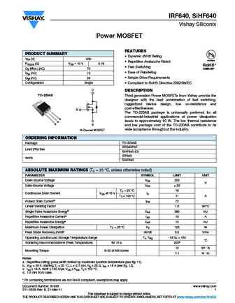
IRF640, SiHF640 Vishay Siliconix Power MOSFET FEATURES PRODUCT SUMMARY Dynamic dV/dt Rating VDS (V) 200 Available Repetitive Avalanche Rated RDS(on) ( )VGS = 10 V 0.18 RoHS* Fast Switching Qg (Max.) (nC) 70 COMPLIANT Ease of Paralleling Qgs (nC) 13 Qgd (nC) 39 Simple Drive Requirements Configuration Single Compliant to RoHS Directive 2002/95/EC D DESC
si6404dq.pdf
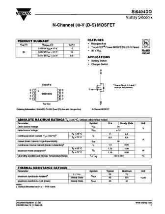
Si6404DQ Vishay Siliconix N-Channel 30-V (D-S) MOSFET FEATURES PRODUCT SUMMARY Halogen-free VDS (V) RDS(on) ( )ID (A) TrenchFET Power MOSFETS 2.5 V Rated 0.009 at VGS = 10 V 11 30 V VDS RoHS 0.010 at VGS = 4.5 V 30 10 COMPLIANT 0.014 at VGS = 2.5 V 8.8 APPLICATIONS Battery Switch Charger Switch D TSSOP-8 * Source Pins 2, 3, 6 and 7 must be

sihl640s.pdf

IRL640S, SiHL640S Vishay Siliconix Power MOSFET FEATURES PRODUCT SUMMARY Halogen-free According to IEC 61249-2-21 VDS (V) 200 Definition Surface Mount RDS(on) ( )VGS = 5 V 0.18 Available in Tape and Reel Qg (Max.) (nC) 66 Dynamic dV/dt Rating Repetitive Avalanche Rated Qgs (nC) 9.0 Logic-Level Gate Drive Qgd (nC) 38 RDS(on) Specified at VGS = 4 V a
irf640 sihf640.pdf

IRF640, SiHF640 Vishay Siliconix Power MOSFET FEATURES PRODUCT SUMMARY Dynamic dV/dt Rating VDS (V) 200 Available Repetitive Avalanche Rated RDS(on) ( )VGS = 10 V 0.18 RoHS* Fast Switching Qg (Max.) (nC) 70 COMPLIANT Ease of Paralleling Qgs (nC) 13 Qgd (nC) 39 Simple Drive Requirements Configuration Single Compliant to RoHS Directive 2002/95/EC D DESC
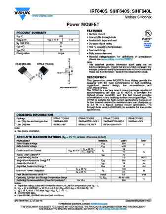
dmg6402ldm.pdf
DMG6402LDM N-CHANNEL ENHANCEMENT MODE MOSFET Please click here to visit our online spice models database. Features Mechanical Data Low RDS(ON) Case SOT-26 Case Material - Molded Plastic. UL Flammability Rating 94V-0 Low Input Capacitance Moisture Sensitivity Level 1 per J-STD-020 Fast Switching Speed Terminals Finish - Matte Tin Solderable per MIL-S
dmg6402lvt.pdf
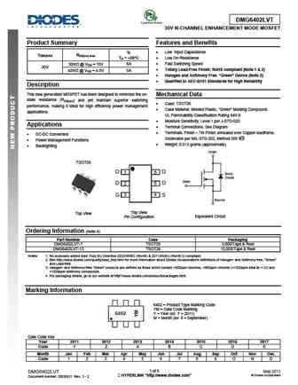
DMG6402LVT 30V N-CHANNEL ENHANCEMENT MODE MOSFET Product Summary Features and Benefits ID Low Input Capacitance V(BR)DSS RDS(on) max TA = +25 C Low On-Resistance Fast Switching Speed 30m @ VGS = 10V 6A 30V Totally Lead-Free Finish; RoHS compliant (Note 1 & 2) 42m @ VGS = 4.5V 5A Halogen and Antimony Free. Green Device (Note 3) Qualified
bfp640esd.pdf
BFP640ESD Surface mount robust silicon NPN RF bipolar transistor Product description The BFP640ESD is a RF bipolar transistor based on SiGe C technology that is part of Infineon s established sixth generation transistor family. Its ESD structure, high RF gain and low noise figure characteristics make the device suitable for a wide range of wireless applications. It remains cost competit
irgs4640dpbf irgsl4640dpbf irgb4640dpbf irgp4640dpbf irgp4640d-epbf.pdf

IRGS4640DPbF IRGSL4640DPbF IRGB4640DPbF IRGP4640D(-E)PbF Insulated Gate Bipolar Transistor with Ultrafast Soft Recovery Diode VCES = 600V C IC = 40A, TC =100 C E E E E tSC 5 s, TJ(max) = 175 C E G C C C C C G G G G G E IRGP4640D-EPbF VCE(ON) typ. = 1.60V @ IC = 24A IRGS4640DPbF IRGP4640DPbF IRGSL4640DPbF IRGB4640DPbF TO-247AD D2Pak TO-247AC
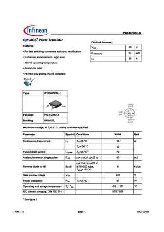
ipd640n06lg ipd640n06l g.pdf
% # ! % (>.;?6?@ %>E Features D P ?A 61BC BF9C389>7 3?>E5AC5AB 1>4 BH>3 A53C96931C9?> 4 mW D n) m x P ( 381>>581>35=5>C
bfp640.pdf
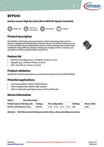
BFP640 Surface mount high linearity silicon NPN RF bipolar transistor Product description The BFP640 is a RF bipolar transistor based on SiGe C technology that is part of Infineon s established sixth generation transistor family. Its transition frequency fT of 42 GHz and high linearity characteristics at low currents make this device particularly suitable for energy efficiency designs a
om6405sd.pdf
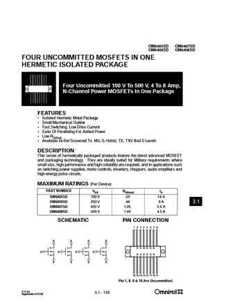
OM6405SD OM6407SD OM6406SD OM6408SD FOUR UNCOMMITTED MOSFETS IN ONE HERMETIC ISOLATED PACKAGE Four Uncommitted 100 V To 500 V, 4 To 8 Amp, N-Channel Power MOSFETs In One Package FEATURES Isolated Hermetic Metal Package Small Mechanical Outline Fast Switching, Low Drive Current Ease Of Paralleling For Added Power Low RDS(on) Available Hi-Rel Screened To MIL-S-
huf76407d3s.pdf

Is Now Part of To learn more about ON Semiconductor, please visit our website at www.onsemi.com Please note As part of the Fairchild Semiconductor integration, some of the Fairchild orderable part numbers will need to change in order to meet ON Semiconductor s system requirements. Since the ON Semiconductor product management systems do not have the ability to manage part nomenclatur
irls640a.pdf

Is Now Part of To learn more about ON Semiconductor, please visit our website at www.onsemi.com Please note As part of the Fairchild Semiconductor integration, some of the Fairchild orderable part numbers will need to change in order to meet ON Semiconductor s system requirements. Since the ON Semiconductor product management systems do not have the ability to manage part nomenclatur
fdc6401n.pdf

Is Now Part of To learn more about ON Semiconductor, please visit our website at www.onsemi.com Please note As part of the Fairchild Semiconductor integration, some of the Fairchild orderable part numbers will need to change in order to meet ON Semiconductor s system requirements. Since the ON Semiconductor product management systems do not have the ability to manage part nomenclatur
bc640-016g.pdf
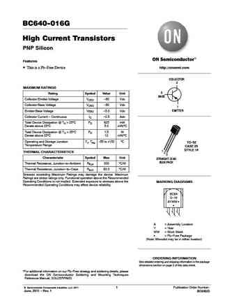
BC640-016G High Current Transistors PNP Silicon Features This is a Pb-Free Device http //onsemi.com COLLECTOR 2 MAXIMUM RATINGS 3 Rating Symbol Value Unit BASE Collector-Emitter Voltage VCEO -80 Vdc Collector-Base Voltage VCBO -80 Vdc 1 Emitter-Base Voltage VEBO -5.0 Vdc EMITTER Collector Current - Continuous IC -0.5 Adc Total Device Dissipation @ TA = 25 C PD 625 mW Derat
irl640a.pdf

Is Now Part of To learn more about ON Semiconductor, please visit our website at www.onsemi.com Please note As part of the Fairchild Semiconductor integration, some of the Fairchild orderable part numbers will need to change in order to meet ON Semiconductor s system requirements. Since the ON Semiconductor product management systems do not have the ability to manage part nomenclatur
bc640ta.pdf

Is Now Part of To learn more about ON Semiconductor, please visit our website at www.onsemi.com Please note As part of the Fairchild Semiconductor integration, some of the Fairchild orderable part numbers will need to change in order to meet ON Semiconductor s system requirements. Since the ON Semiconductor product management systems do not have the ability to manage part nomenclatur
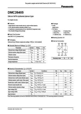
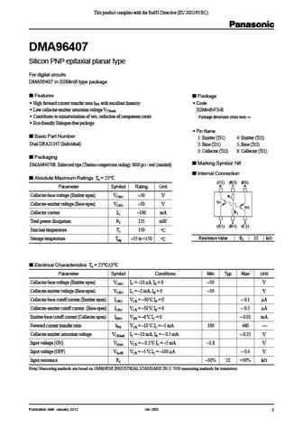
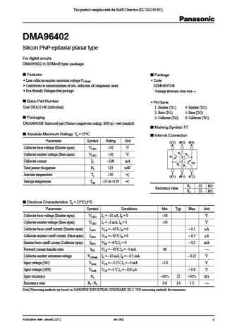
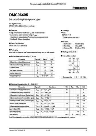
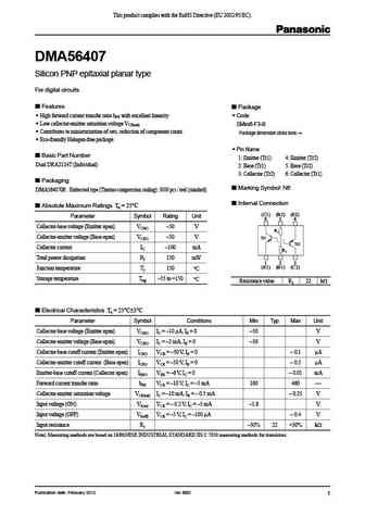
dmc96407.pdf

This product complies with the RoHS Directive (EU 2002/95/EC). DMC96407 Silicon NPN epitaxial planar type For digital circuits DMC56407 in SSMini6 type package Package Features High forward current transfer ratio hFE with excellent linearity Code Low collector-emitter saturation voltage VCE(sat) SSMini6-F3-B Contributes to miniaturization of sets, reduction o
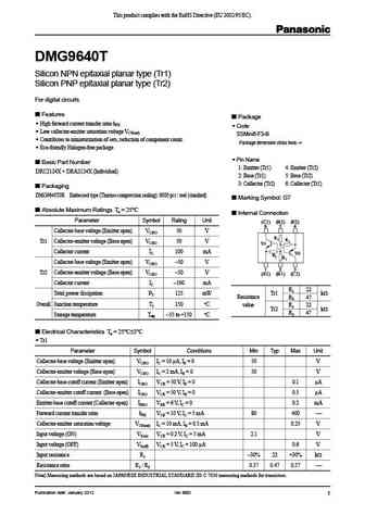
dmg96401.pdf
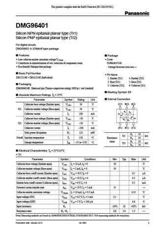
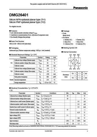
This product complies with the RoHS Directive (EU 2002/95/EC). DMG96401 Silicon NPN epitaxial planar type (Tr1) Silicon PNP epitaxial planar type (Tr2) For digital circuits DMG56401 in SSMini6 type package Features Package Low collector-emitter saturation voltage VCE(sat) Code Contributes to miniaturization of sets, reduction of component count. SSMini6-F3-B E
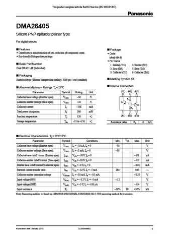
dma56404.pdf

This product complies with the RoHS Directive (EU 2002/95/EC). DMA56404 Silicon PNP epitaxial planar type For digital circuits DMA26404 in SMini6 type package Features Package Low collector-emitter saturation voltage VCE(sat) Code Contributes to miniaturization of sets, reduction of component count. SMini6-F3-B Eco-friendly Halogen-free package Package dimensi
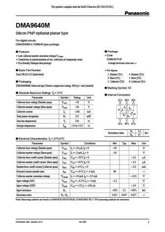
dma5640m.pdf
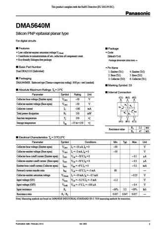
This product complies with the RoHS Directive (EU 2002/95/EC). DMA5640M Silicon PNP epitaxial planar type For digital circuits Features Package Low collector-emitter saturation voltage VCE(sat) Code Contributes to miniaturization of sets, reduction of component count. SMini6-F3-B Eco-friendly Halogen-free package Package dimension clicks here. Click!
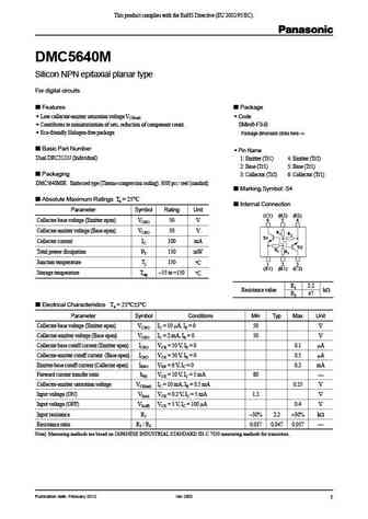
dmc5640l.pdf
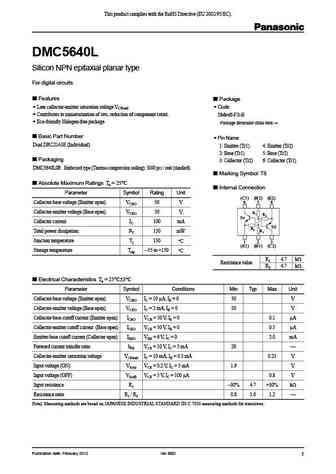
This product complies with the RoHS Directive (EU 2002/95/EC). DMC5640L Silicon NPN epitaxial planar type For digital circuits Features Package Low collector-emitter saturation voltage VCE(sat) Code Contributes to miniaturization of sets, reduction of component count. SMini6-F3-B Eco-friendly Halogen-free package Package dimension clicks here. Click! Ba

dmc9640n.pdf
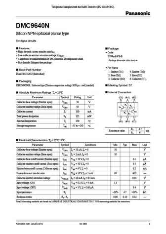
This product complies with the RoHS Directive (EU 2002/95/EC). DMC9640N Silicon NPN epitaxial planar type For digital circuits Features Package High forward current transfer ratio hFE Code Low collector-emitter saturation voltage VCE(sat) SSMini6-F3-B Contributes to miniaturization of sets, reduction of component count. Package dimension clicks here. Click
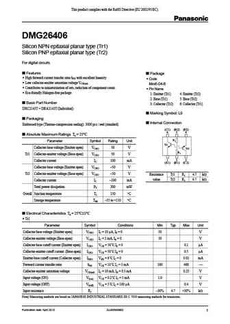
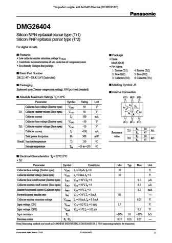
dmg9640t.pdf
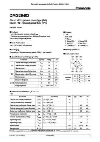
This product complies with the RoHS Directive (EU 2002/95/EC). DMG9640T Silicon NPN epitaxial planar type (Tr1) Silicon PNP epitaxial planar type (Tr2) For digital circuits Features Package High forward current transfer ratio hFE Code Low collector-emitter saturation voltage VCE(sat) SSMini6-F3-B Contributes to miniaturization of sets, reduction of component
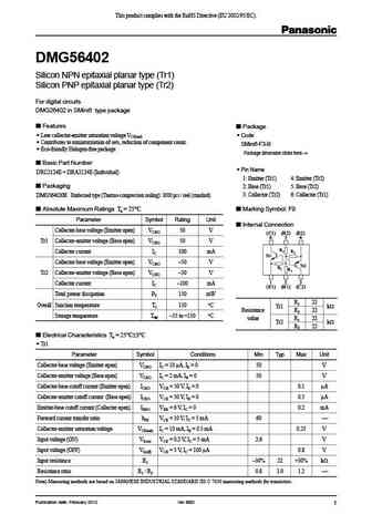
dmc96402.pdf

This product complies with the RoHS Directive (EU 2002/95/EC). DMC96402 Silicon NPN epitaxial planar type For digital circuits DMC56402 in SSMini6 type package Features Package Low collector-emitter saturation voltage VCE(sat) Code Contributes to miniaturization of sets, reduction of component count. SSMini6-F3-B Eco-friendly Halogen-free package Package dimen
2sk066400l.pdf
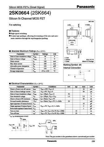
Silicon MOS FETs (Small Signal) 2SK0664 (2SK664) Silicon N-Channel MOS FET unit mm 0.15+0.10 0.3+0.1 0.05 For switching 0.0 3 Features High-speed switching S-mini type package, allowing downsizing of the sets and auto- 1 2 matic insertion through the tape/magazine packing. (0.65) (0.65) 1.3 0.1 2.0 0.2 10 Absolute Maximum Ratings (Ta = 25 C) Parameter Symbol R
dmc56406.pdf

This product complies with the RoHS Directive (EU 2002/95/EC). DMC56406 Silicon NPN epitaxial planar type For digital circuits DMC26406 in SMini6 type package Package Features Code High forward current transfer ratio hFE with excellent linearity Low collector-emitter saturation voltage VCE(sat) SMini6-F3-B Contributes to miniaturization of sets, reduction of co
dma56406.pdf

This product complies with the RoHS Directive (EU 2002/95/EC). DMA56406 Silicon PNP epitaxial planar type For digital circuits DMA26406 in SMini6 type package Features Package High forward current transfer ratio hFE with excellent linearity Code SMini6-F3-B Low collector-emitter saturation voltage VCE(sat) Contributes to miniaturization of sets, reduction of co
dma26406.pdf

This product complies with the RoHS Directive (EU 2002/95/EC). DMA26406 Silicon PNP epitaxial planar type For digital circuits Features Package Contributes to miniaturization of sets, reduction of component count. Code Eco-friendly Halogen-free package Mini6-G4-B Pin Name Basic Part Number 1 Emitter (Tr1) 4 Emitter (Tr2) Dual DRA2143T (Individual)
dma96407.pdf
This product complies with the RoHS Directive (EU 2002/95/EC). DMA96407 Silicon PNP epitaxial planar type For digital circuits DMA56407 in SSMini6 type package Features Package High forward current transfer ratio hFE with excellent linearity Code Low collector-emitter saturation voltage VCE(sat) SSMini6-F3-B Contributes to miniaturization of sets, reduction of
dmg96403.pdf

This product complies with the RoHS Directive (EU 2002/95/EC). DMG96403 Silicon NPN epitaxial planar type (Tr1) Silicon PNP epitaxial planar type (Tr2) For digital circuits DMG56403 in SSMini6 type package Features Package Low collector-emitter saturation voltage VCE(sat) Code Contributes to miniaturization of sets, reduction of component count. SSMini6-F3-B
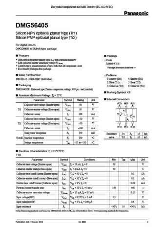
dmc56405.pdf

This product complies with the RoHS Directive (EU 2002/95/EC). DMC56405 Silicon NPN epitaxial planar type For digital circuits DMC26405 in SMini6 type package Features Package High forward current transfer ratio hFE with excellent linearity Code Low collector-emitter saturation voltage VCE(sat) SMini6-F3-B Contributes to miniaturization of sets, reduction of co
dmg56405.pdf
This product complies with the RoHS Directive (EU 2002/95/EC). DMG56405 Silicon NPN epitaxial planar type (Tr1) Silicon PNP epitaxial planar type (Tr2) For digital circuits DMG26405 in SMini6 type package Features Package High forward current transfer ratio hFE with excellent linearity Code Low collector-emitter saturation voltage VCE(sat) SMini6-F3-B Contri
dmg96404.pdf

This product complies with the RoHS Directive (EU 2002/95/EC). DMG96404 Silicon NPN epitaxial planar type (Tr1) Silicon PNP epitaxial planar type (Tr2) For digital circuits DMG56404 in SSMini6 type package Features Package Low collector-emitter saturation voltage VCE(sat) Code Contributes to miniaturization of sets, reduction of component count. SSMini6-F3-B Eco
dmc96406.pdf
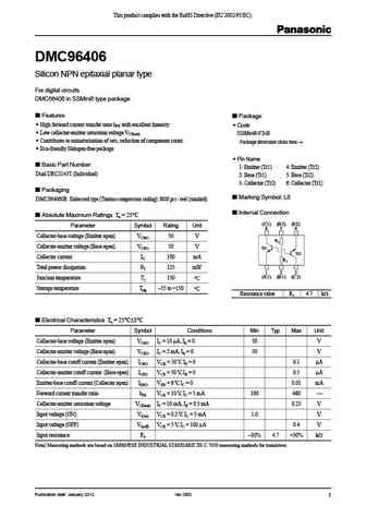
This product complies with the RoHS Directive (EU 2002/95/EC). DMC96406 Silicon NPN epitaxial planar type For digital circuits DMC56406 in SSMini6 type package Features Package High forward current transfer ratio hFE with excellent linearity Code Low collector-emitter saturation voltage VCE(sat) SSMini6-F3-B Contributes to miniaturization of sets, reduction o
dmg9640n.pdf

This product complies with the RoHS Directive (EU 2002/95/EC). DMG9640N Silicon NPN epitaxial planar type (Tr1) Silicon PNP epitaxial planar type (Tr2) For digital circuits DMG5640N in SSMini6 type package Features Package High forward current transfer ratio hFE Code Low collector-emitter saturation voltage VCE(sat) SSMini6-F3-B Contributes to miniaturization
dmc96400.pdf

This product complies with the RoHS Directive (EU 2002/95/EC). DMC96400 Silicon NPN epitaxial planar type For digital circuits DMC56400 in SSMini6 type package Features Package High forward current transfer ratio hFE with excellent linearity Code Low collector-emitter saturation voltage VCE(sat) SSMini6-F3-B Contributes to miniaturization of sets, reduction o
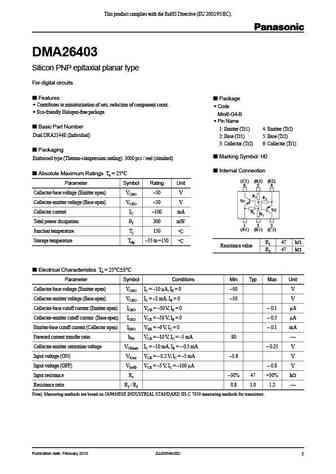
dma56403.pdf
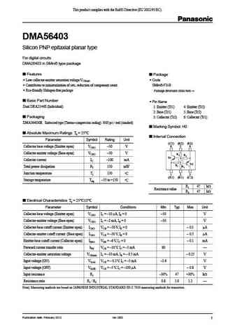
This product complies with the RoHS Directive (EU 2002/95/EC). DMA56403 Silicon PNP epitaxial planar type For digital circuits DMA26403 in SMini6 type package Features Package Low collector-emitter saturation voltage VCE(sat) Code Contributes to miniaturization of sets, reduction of component count. SMini6-F3-B Eco-friendly Halogen-free package Click! Click!
dma96403.pdf
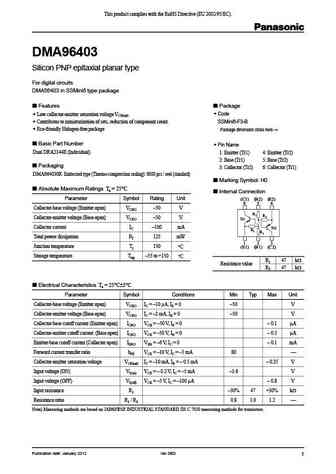
This product complies with the RoHS Directive (EU 2002/95/EC). DMA96403 Silicon PNP epitaxial planar type For digital circuits DMA56403 in SSMini6 type package Package Features Code Low collector-emitter saturation voltage VCE(sat) Contributes to miniaturization of sets, reduction of component count. SSMini6-F3-B Eco-friendly Halogen-free package Package dimen
dma96406.pdf
This product complies with the RoHS Directive (EU 2002/95/EC). DMA96406 Silicon PNP epitaxial planar type For digital circuits DMA56406 in SSMini6 type package Features Package High forward current transfer ratio hFE with excellent linearity Code Low collector-emitter saturation voltage VCE(sat) SSMini6-F3-B Contributes to miniaturization of sets, reduction of co
dmc26404.pdf

This product complies with the RoHS Directive (EU 2002/95/EC). DMC26404 Silicon NPN epitaxial planar type For digital circuits Features Package Low collector-emitter saturation voltage VCE(sat) Code Contributes to miniaturization of sets, reduction of component count. Mini6-G4-B Eco-friendly Halogen-free package Pin Name 1 Emitter (Tr1) 4 Emitter (Tr2
dmg96405.pdf

This product complies with the RoHS Directive (EU 2002/95/EC). DMG96405 Silicon NPN epitaxial planar type (Tr1) Silicon PNP epitaxial planar type (Tr2) For digital circuits DMG56405 in SSMini6 type package Features Package High forward current transfer ratio hFE with excellent linearity Code Low collector-emitter saturation voltage VCE(sat) SSMini6-F3-B Cont
dmg26405.pdf

This product complies with the RoHS Directive (EU 2002/95/EC). DMG26405 Silicon NPN epitaxial planar type (Tr1) Silicon PNP epitaxial planar type (Tr2) For digital circuits Features Package High forward current transfer ratio hFE with excellent linearity Code Low collector-emitter saturation voltage VCE(sat) Mini6-G4-B Contributes to miniaturization of sets, r
dma56401.pdf

This product complies with the RoHS Directive (EU 2002/95/EC). DMA56401 Silicon PNP epitaxial planar type For digital circuits DMA26401 in SMini6 type package Features Package Low collector-emitter saturation voltage VCE(sat) Code Contributes to miniaturization of sets, reduction of component count. SMini6-F3-B Eco-friendly Halogen-free package Package dimensi
dmc2640f.pdf

This product complies with the RoHS Directive (EU 2002/95/EC). DMC2640F Silicon NPN epitaxial planar type For digital circuits Features Package Low collector-emitter saturation voltage VCE(sat) Code Contributes to miniaturization of sets, reduction of component count. Mini6-G4-B Eco-friendly Halogen-free package Pin Name 1 Emitter (Tr1) 4 Emitter (Tr2
dmg96406.pdf
This product complies with the RoHS Directive (EU 2002/95/EC). DMG96406 Silicon NPN epitaxial planar type (Tr1) Silicon PNP epitaxial planar type (Tr2) For digital circuits DMG56406 in SSMini6 type package Features Package High forward current transfer ratio hFE with excellent linearity Code Low collector-emitter saturation voltage VCE(sat) SSMini6-F3-B Contribu
dmc56400.pdf

This product complies with the RoHS Directive (EU 2002/95/EC). DMC56400 Silicon NPN epitaxial planar type For digital circuits DMC26400 in SMini6 type package Features Package High forward current transfer ratio hFE with excellent linearity Code Low collector-emitter saturation voltage VCE(sat) SMini6-F3-B Contributes to miniaturization of sets, reduction of co
dma96401.pdf

This product complies with the RoHS Directive (EU 2002/95/EC). DMA96401 Silicon PNP epitaxial planar type For digital circuits DMA56401 in SSMini6 type package Features Package Low collector-emitter saturation voltage VCE(sat) Code Contributes to miniaturization of sets, reduction of component count. SSMini6-F3-B Eco-friendly Halogen-free package Package dimen
dmg56406.pdf

This product complies with the RoHS Directive (EU 2002/95/EC). DMG56406 Silicon NPN epitaxial planar type (Tr1) Silicon PNP epitaxial planar type (Tr2) For digital circuits DMG26406 in SMini6 type package Features Package High forward current transfer ratio hFE with excellent linearity Code Low collector-emitter saturation voltage VCE(sat) SMini6-F3-B Contri
dmg96402.pdf

This product complies with the RoHS Directive (EU 2002/95/EC). DMG96402 Silicon NPN epitaxial planar type (Tr1) Silicon PNP epitaxial planar type (Tr2) For digital circuits DMG56402 in SSMini6 type package Features Package Low collector-emitter saturation voltage VCE(sat) Code Contributes to miniaturization of sets, reduction of component count. SSMini6-F3-B
dma26403.pdf
This product complies with the RoHS Directive (EU 2002/95/EC). DMA26403 Silicon PNP epitaxial planar type For digital circuits Features Package Contributes to miniaturization of sets, reduction of component count. Code Eco-friendly Halogen-free package Mini6-G4-B Pin Name Basic Part Number 1 Emitter (Tr1) 4 Emitter (Tr2) Dual DRA2144E (Individual)
dmc2640l.pdf

This product complies with the RoHS Directive (EU 2002/95/EC). DMC2640L Silicon NPN epitaxial planar type For digital circuits Features Package Low collector-emitter saturation voltage VCE(sat) Code Contributes to miniaturization of sets, reduction of component count. Mini6-G4-B Eco-friendly Halogen-free package Pin Name 1 Emitter (Tr1) 4 Emitter (Tr2
dmc26401.pdf

This product complies with the RoHS Directive (EU 2002/95/EC). DMC26401 Silicon NPN epitaxial planar type For digital circuits Features Package Low collector-emitter saturation voltage VCE(sat) Code Contributes to miniaturization of sets, reduction of component count. Mini6-G4-B Eco-friendly Halogen-free package Pin Name 1 Emitter (Tr1) 4 Emitter (Tr2
dmg26406.pdf
This product complies with the RoHS Directive (EU 2002/95/EC). DMG26406 Silicon NPN epitaxial planar type (Tr1) Silicon PNP epitaxial planar type (Tr2) For digital circuits Features Package High forward current transfer ratio hFE with excellent linearity Code Low collector-emitter saturation voltage VCE(sat) Mini6-G4-B Contributes to miniaturization of sets, r
dmg56401.pdf

This product complies with the RoHS Directive (EU 2002/95/EC). DMG56401 Silicon NPN epitaxial planar type (Tr1) Silicon PNP epitaxial planar type (Tr2) For digital circuits DMG26401 in SMini6 type package Features Package Low collector-emitter saturation voltage VCE(sat) Code Contributes to miniaturization of sets, reduction of component count. SMini6-F3-B Eco
dmc96401.pdf

This product complies with the RoHS Directive (EU 2002/95/EC). DMC96401 Silicon NPN epitaxial planar type For digital circuits DMC56401 in SSMini6 type package Package Features Code Low collector-emitter saturation voltage VCE(sat) Contributes to miniaturization of sets, reduction of component count. SSMini6-F3-B Eco-friendly Halogen-free package Package dimen
dmc96404.pdf

This product complies with the RoHS Directive (EU 2002/95/EC). DMC96404 Silicon NPN epitaxial planar type For digital circuits DMC56404 in SSMini6 type package Features Package Low collector-emitter saturation voltage VCE(sat) Code Contributes to miniaturization of sets, reduction of component count. SSMini6-F3-B Eco-friendly Halogen-free package Package dimen
dmc56402.pdf

This product complies with the RoHS Directive (EU 2002/95/EC). DMC56402 Silicon NPN epitaxial planar type For digital circuits DMC26402 in SMini6 type package Features Package Low collector-emitter saturation voltage VCE(sat) Code Contributes to miniaturization of sets, reduction of component count. SMini6-F3-B Eco-friendly Halogen-free package Package dimensi
dma26401.pdf

This product complies with the RoHS Directive (EU 2002/95/EC). DMA26401 Silicon PNP epitaxial planar type For digital circuits Features Package Contributes to miniaturization of sets, reduction of component count. Code Eco-friendly Halogen-free package Mini6-G4-B Pin Name Basic Part Number 1 Emitter (Tr1) 4 Emitter (Tr2) Dual DRA2114E (Individual)
dma26402.pdf

This product complies with the RoHS Directive (EU 2002/95/EC). DMA26402 Silicon PNP epitaxial planar type For digital circuits Features Package Contributes to miniaturization of sets, reduction of component count. Code Eco-friendly Halogen-free package Mini6-G4-B Pin Name Basic Part Number 1 Emitter (Tr1) 4 Emitter (Tr2) Dual DRA2124E (Individual)
dma56402.pdf

This product complies with the RoHS Directive (EU 2002/95/EC). DMA56402 Silicon PNP epitaxial planar type For digital circuits DMA26402 in SMini6 type package Features Package Low collector-emitter saturation voltage VCE(sat) Code Contributes to miniaturization of sets, reduction of component count. SMini6-F3-B Eco-friendly Halogen-free package Package dimensi
dmg5640n.pdf
This product complies with the RoHS Directive (EU 2002/95/EC). DMG5640N Silicon NPN epitaxial planar type (Tr1) Silicon PNP epitaxial planar type (Tr2) For digital circuits Features Package High forward current transfer ratio hFE Code Low collector-emitter saturation voltage VCE(sat) SMini6-F3-B Contributes to miniaturization of sets, reduction of component c
dmg5640m.pdf

This product complies with the RoHS Directive (EU 2002/95/EC). DMG5640M Silicon NPN epitaxial planar type (Tr1) Silicon PNP epitaxial planar type (Tr2) For digital circuits Features Package Low collector-emitter saturation voltage VCE(sat) Code Contributes to miniaturization of sets, reduction of component count. SMini6-F3-B Eco-friendly Halogen-free package
dmc26403.pdf

This product complies with the RoHS Directive (EU 2002/95/EC). DMC26403 Silicon NPN epitaxial planar type For digital circuits Features Package Low collector-emitter saturation voltage VCE(sat) Code Contributes to miniaturization of sets, reduction of component count. Mini6-G4-B Eco-friendly Halogen-free package Pin Name 1 Emitter (Tr1) 4 Emitter (Tr2
dma26405.pdf
This product complies with the RoHS Directive (EU 2002/95/EC). DMA26405 Silicon PNP epitaxial planar type For digital circuits Features Package Contributes to miniaturization of sets, reduction of component count. Code Eco-friendly Halogen-free package Mini6-G4-B Pin Name Basic Part Number 1 Emitter (Tr1) 4 Emitter (Tr2) Dual DRA2114T (Individual)

dma9640m.pdf
This product complies with the RoHS Directive (EU 2002/95/EC). DMA9640M Silicon PNP epitaxial planar type For digital circuits DMA5640M in SSMini6 type package Package Features Code Low collector-emitter saturation voltage VCE(sat) SSMini6-F3-B Contributes to miniaturization of sets, reduction of component count. Eco-friendly Halogen-free package Package dime
dmc5640m.pdf
This product complies with the RoHS Directive (EU 2002/95/EC). DMC5640M Silicon NPN epitaxial planar type For digital circuits Features Package Low collector-emitter saturation voltage VCE(sat) Code Contributes to miniaturization of sets, reduction of component count. SMini6-F3-B Eco-friendly Halogen-free package Package dimension clicks here. Click! Basi
dmg56403.pdf

This product complies with the RoHS Directive (EU 2002/95/EC). DMG56403 Silicon NPN epitaxial planar type (Tr1) Silicon PNP epitaxial planar type (Tr2) For digital circuits Features Package Low collector-emitter saturation voltage VCE(sat) Code Contributes to miniaturization of sets, reduction of component count. SMini6-F3-B Eco-friendly Halogen-free package P
dmc96403.pdf

This product complies with the RoHS Directive (EU 2002/95/EC). DMC96403 Silicon NPN epitaxial planar type For digital circuits DMC56403 in SSMini6 type package Features Package Low collector-emitter saturation voltage VCE(sat) Code Contributes to miniaturization of sets, reduction of component count. SSMini6-F3-B Eco-friendly Halogen-free package Package dim
dmc56407.pdf

This product complies with the RoHS Directive (EU 2002/95/EC). DMC56407 Silicon NPN epitaxial planar type For digital circuits Package Features Code High forward current transfer ratio hFE with excellent linearity Low collector-emitter saturation voltage VCE(sat) SMini6-F3-B Contributes to miniaturization of sets, reduction of component count. Package dimension
dma56405.pdf

This product complies with the RoHS Directive (EU 2002/95/EC). DMA56405 Silicon PNP epitaxial planar type For digital circuits DMA26405 in SMini6 type package Features Package High forward current transfer ratio hFE with excellent linearity Code Low collector-emitter saturation voltage VCE(sat) SMini6-F3-B Contributes to miniaturization of sets, reduction of co
dma96402.pdf
This product complies with the RoHS Directive (EU 2002/95/EC). DMA96402 Silicon PNP epitaxial planar type For digital circuits DMA56402 in SSMini6 type package Features Package Low collector-emitter saturation voltage VCE(sat) Code Contributes to miniaturization of sets, reduction of component count. SSMini6-F3-B Eco-friendly Halogen-free package Package dimen
dmc96405.pdf
This product complies with the RoHS Directive (EU 2002/95/EC). DMC96405 Silicon NPN epitaxial planar type For digital circuits DMC56405 in SSMini6 type package Features Package High forward current transfer ratio hFE with excellent linearity Code Low collector-emitter saturation voltage VCE(sat) SSMini6-F3-B Contributes to miniaturization of sets, reduction of
dmc26402.pdf

This product complies with the RoHS Directive (EU 2002/95/EC). DMC26402 Silicon NPN epitaxial planar type For digital circuits Features Package Low collector-emitter saturation voltage VCE(sat) Code Contributes to miniaturization of sets, reduction of component count. Mini6-G4-B Eco-friendly Halogen-free package Pin Name 1 Emitter (Tr1) 4 Emitter (Tr2
dmg9640m.pdf

This product complies with the RoHS Directive (EU 2002/95/EC). DMG9640M Silicon NPN epitaxial planar type (Tr1) Silicon PNP epitaxial planar type (Tr2) For digital circuits DMG5640M in SSMini6 type package Features Package Low collector-emitter saturation voltage VCE(sat) Code Contributes to miniaturization of sets, reduction of component count. SSMini6-F3-B
dma56407.pdf
This product complies with the RoHS Directive (EU 2002/95/EC). DMA56407 Silicon PNP epitaxial planar type For digital circuits Features Package High forward current transfer ratio hFE with excellent linearity Code Low collector-emitter saturation voltage VCE(sat) SMini6-F3-B Contributes to miniaturization of sets, reduction of component count. Package dimensi
dmg56402.pdf
This product complies with the RoHS Directive (EU 2002/95/EC). DMG56402 Silicon NPN epitaxial planar type (Tr1) Silicon PNP epitaxial planar type (Tr2) For digital circuits DMG26402 in SMini6 type package Features Package Low collector-emitter saturation voltage VCE(sat) Code Contributes to miniaturization of sets, reduction of component count. SMini6-F3-B Eco
dmc56401.pdf

This product complies with the RoHS Directive (EU 2002/95/EC). DMC56401 Silicon NPN epitaxial planar type For digital circuits DMC26401 in SMini6 type package Features Package Low collector-emitter saturation voltage VCE(sat) Code Contributes to miniaturization of sets, reduction of component count. SMini6-F3-B Eco-friendly Halogen-free package Package dimensi

dmg56404.pdf

This product complies with the RoHS Directive (EU 2002/95/EC). DMG56404 Silicon NPN epitaxial planar type (Tr1) Silicon PNP epitaxial planar type (Tr2) For digital circuits DMG26404 in SMini6 type package Features Package Low collector-emitter saturation voltage VCE(sat) Code Contributes to miniaturization of sets, reduction of component count. SMini6-F3-B E
dmc56404.pdf

This product complies with the RoHS Directive (EU 2002/95/EC). DMC56404 Silicon NPN epitaxial planar type For digital circuits DMC26404 in SMini6 type package Features Package Low collector-emitter saturation voltage VCE(sat) Code Contributes to miniaturization of sets, reduction of component count. SMini6-F3-B Eco-friendly Halogen-free package Package dimensi
dmc56403.pdf

This product complies with the RoHS Directive (EU 2002/95/EC). DMC56403 Silicon NPN epitaxial planar type For digital circuits DMC26403 in SMini6 type package Features Package Low collector-emitter saturation voltage VCE(sat) Code Contributes to miniaturization of sets, reduction of component count. SMini6-F3-B Eco-friendly Halogen-free package Package dimensi
tn2640pss.pdf
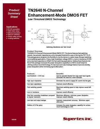
Product TN2640 N-Channel Summary Enhancement-Mode DMOS FET Sheet Low Threshold DMOS Technology Applications DC-DC converters Solid state relays Ultrasound pulsers Telecom switches Photo voltaic drivers Analog switches Switching Waveforms and Test Circuit Product Overview TN2640K4 N-Channel Enhancement-Mode DMOS FET. The device features fast switching speeds, low parasitic
tn2640.pdf
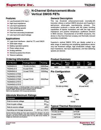
Supertex inc. TN2640 N-Channel Enhancement-Mode Vertical DMOS FETs Features General Description This low threshold enhancement-mode (normally-off) Low threshold (2.0V max.) transistor utilizes a vertical DMOS structure and Supertex s High input impedance well-proven silicon-gate manufacturing process. This Low input capacitance combination produces a device with the po
tp2640.pdf
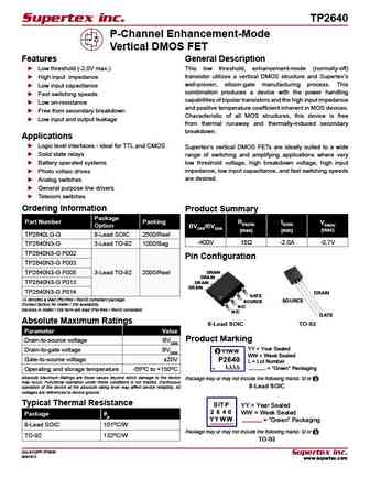
Supertex inc. TP2640 P-Channel Enhancement-Mode Vertical DMOS FET Features General Description Low threshold (-2.0V max.) This low threshold, enhancement-mode (normally-off) transistor utilizes a vertical DMOS structure and Supertex s High input impedance well-proven, silicon-gate manufacturing process. This Low input capacitance combination produces a device with the po
ut6402.pdf
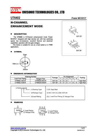
UNISONIC TECHNOLOGIES CO., LTD UT6402 Power MOSFET N-CHANNEL ENHANCEMENT MODE 3 1 DESCRIPTION 2 SOT-23 The UT6402 is N-Channel enhancement mode Power MOSFET, designed with high density cell, with fast switching 4 speed, low on-resistance, excellent thermal and electrical 5 capabilities, operation with low gate voltages. 6 This device is suitable for use as a load swit
uf9640.pdf
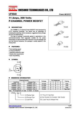
UNISONIC TECHNOLOGIES CO., LTD UF9640 Power MOSFET 11 Amps, 200 Volts P-CHANNEL POWER MOSFET DESCRIPTION The UF9640 is a P-channel Power MOSFET that developed by UTC s advanced technlogy. The device has an advantage of including fast switching, low on-resistance, ruggedized device design and low cost-effectiveness. This type of package is generally applied in applicat
uf640g-aa3-r uf640l-ta3-t uf640g-ta3-t uf640l-tf1-t uf640g-tf1-t uf640l-tf2-t uf640g-tf2-t uf640l-tf3-t uf640g-tf3-t.pdf
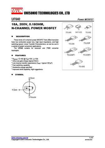
UNISONIC TECHNOLOGIES CO., LTD UF640 Power MOSFET 18A, 200V, 0.18OHM, N-CHANNEL POWER MOSFET DESCRIPTION These kinds of n-channel power MOSFET field effect transistor have low conduction power loss, high input impedance, and high switching speed, Linear Transfer Characteristics, so can be use in a variety of power conversion applications. The UF640 suitable for resonant an
ut6401.pdf
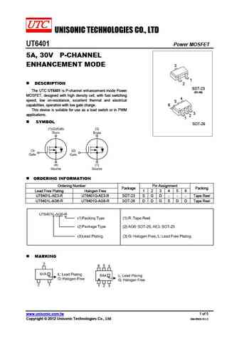
UNISONIC TECHNOLOGIES CO., LTD UT6401 Power MOSFET 5A, 30V P-CHANNEL ENHANCEMENT MODE 3 1 DESCRIPTION 2 SOT-23 The UTC UT6401 is P-channel enhancement mode Power (SC-59) MOSFET, designed with high density cell, with fast switching 4 speed, low on-resistance, excellent thermal and electrical 5 capabilities, operation with low gate charge. 6 This device is suitable for u
uf640l-tn3-r uf640g-tn3-r uf640l-t2q-t uf640g-t2q-t uf640l-t2q-r uf640g-t2q-r uf640l-tq2-t uf640g-tq2-t uf640l-tq2-r uf640g-tq2-r.pdf

UNISONIC TECHNOLOGIES CO., LTD UF640 Power MOSFET 18A, 200V, 0.18OHM, N-CHANNEL POWER MOSFET DESCRIPTION These kinds of n-channel power MOSFET field effect transistor have low conduction power loss, high input impedance, and high switching speed, Linear Transfer Characteristics, so can be use in a variety of power conversion applications. The UF640 suitable for resonant an
uf640.pdf
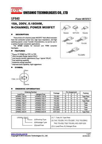
UNISONIC TECHNOLOGIES CO., LTD UF640 Power MOSFET 18A, 200V, 0.18OHM, N-CHANNEL POWER MOSFET DESCRIPTION These kinds of n-channel power MOSFET field effect transistor have low conduction power loss, high input impedance, and high switching speed, Linear Transfer Characteristics, so can be use in a variety of power conversion applications. The UF640 suitable for resonant an
2sk2640-01mr.pdf
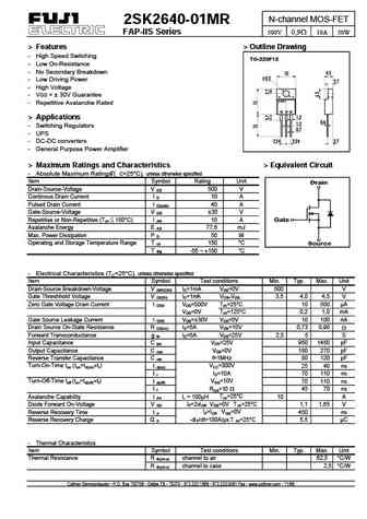
N-channel MOS-FET 2SK2640-01MR FAP-IIS Series 500V 0,9 10A 50W > Features > Outline Drawing - High Speed Switching - Low On-Resistance - No Secondary Breakdown - Low Driving Power - High Voltage - VGS = 30V Guarantee - Repetitive Avalanche Rated > Applications - Switching Regulators - UPS - DC-DC converters - General Purpose Power Amplifier > Maximum Ratings and Characteri
2n7640-ga.pdf
2N7640-GA Normally OFF Silicon Carbide VDS = 650 V Junction Transistor VDS(ON) = 1.7 V ID = 16 A RDS(ON) = 110 m Features Package 250 C maximum operating temperature RoHS Compliant Temperature independent switching performance D Gate oxide free SiC switch S Suitable for connecting an anti-parallel diode Positive temperature coefficient for e
irf640 irf641 irf642 irf643 rf1s640.pdf

IRF640, IRF641, IRF642, S E M I C O N D U C T O R IRF643, RF1S640, RF1S640SM 16A and 18A, 150V and 200V, 0.18 and 0.22 Ohm, N-Channel Power MOSFETs January 1998 Features Description 16A and 18A, 150V and 200V These are N-Channel enhancement mode silicon gate power field effect transistors. They are advanced power rDS(ON) = 0.18 and 0.22 MOSFETs designed, tested, and guar
rf1s640.pdf
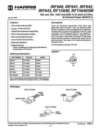
IRF640, IRF641, IRF642, S E M I C O N D U C T O R IRF643, RF1S640, RF1S640SM 16A and 18A, 150V and 200V, 0.18 and 0.22 Ohm, N-Channel Power MOSFETs January 1998 Features Description 16A and 18A, 150V and 200V These are N-Channel enhancement mode silicon gate power field effect transistors. They are advanced power rDS(ON) = 0.18 and 0.22 MOSFETs designed, tested, and guar
huf76409p3.pdf
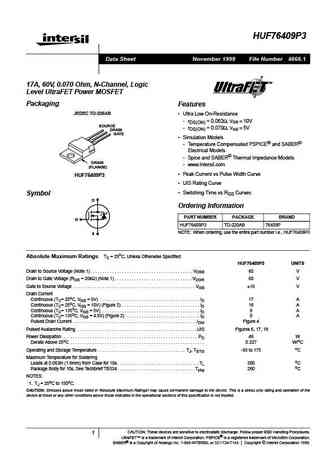
HUF76409P3 Data Sheet November 1999 File Number 4666.1 17A, 60V, 0.070 Ohm, N-Channel, Logic Level UltraFET Power MOSFET Packaging Features JEDEC TO-220AB Ultra Low On-Resistance - rDS(ON) = 0.062 , VGS = 10V SOURCE - rDS(ON) = 0.070 , VGS = 5V DRAIN GATE Simulation Models - Temperature Compensated PSPICE and SABER Electrical Models - Spice and SABER Thermal Im
irfp640.pdf
IRFP640 HEXFET Power MOSFET Dynamic dv/dt Rating Repetitive Avalanche Rated VDSS = 200V Fast switching Ease of Paralleling ID = 18A Simple Drive Requirements RDS(ON) =0.18 Description Third Generation HEXFETs from International Rectifier www.DataSheet4U.com provide the designer with the best combination of fast switching, ruggedized device design, low on-res
stt6405.pdf
STT6405 -5.0 A, -30 V, RDS(ON) 50 m P-Channel Enhancement Mode Mos.FET Elektronische Bauelemente RoHS Compliant Product TSOP-6 A suffix of -C specifies halogen and lead-free DESCRIPTION The STT6405 uses advanced trench technology A E to provide excellent on-resistance with low gate change. L The device is suitable for use as a load switch or in PWM
bc636-638-640.pdf
BC636/638/640 PNP Type Elektronische Bauelemente Plastic Encapsulate Transistors RoHS Compliant Product A suffix of "-C" specifies halogen & lead-free TO-92 FEATURE 4.55 0.2 3.5 0.2 Power Dissipation o PCM 0.83 mW (Tamb=25 C) 08 0.43+0.07 0. 1 0.46+0.1 0. (1.27 Typ. ) 1 Emitter +0.2 1.25 0.2 1 2 3 2 Collector 2.54 0.1 3 Base o MAXIMUM RATINGS (TA
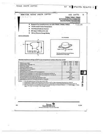
csd16401q5.pdf
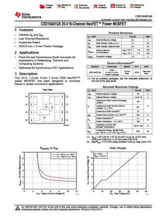
Sample & Support & Reference Product Technical Tools & Buy Community Design Folder Documents Software CSD16401Q5 SLPS200B AUGUST 2009 REVISED SEPTEMBER 2015 CSD16401Q5 25-V N-Channel NexFET Power MOSFET 1 Features Product Summary 1 Ultralow Qg and Qgd TA = 25 C VALUE UNIT Low Thermal Resistance VDS Drain-to-Source voltage 25 V Avalanche Rated Qg Gate Charge,
csd16409q3.pdf
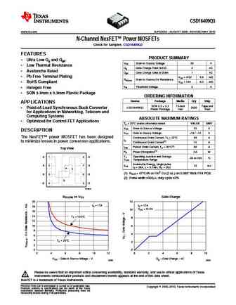
CSD16409Q3 www.ti.com SLPS204A AUGUST 2009 REVISED MAY 2010 N-Channel NexFET Power MOSFETs Check for Samples CSD16409Q3 1 FEATURES PRODUCT SUMMARY 2 Ultra Low Qg and Qgd VDS Drain to Source Voltage 25 V Low Thermal Resistance Qg Gate Charge Total (4.5V) 4 nC Avalanche Rated Qgd Gate Charge Gate to Drain 1 nC Pb Free Terminal Plating VGS = 4.5V 9.5 m
csd16404q5a.pdf
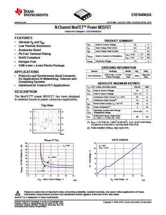
CSD16404Q5A www.ti.com SLPS198B AUGUST 2009 REVISED APRIL 2010 N-Channel NexFET Power MOSFET Check for Samples CSD16404Q5A 1 FEATURES PRODUCT SUMMARY 2 Ultralow Qg and Qgd VDS Drain to Source Voltage 25 V Low Thermal Resistance Qg Gate Charge Total (4.5V) 6.5 nC Avalanche Rated Qgd Gate Charge Gate to Drain 1.7 nC Pb Free Terminal Plating VGS = 4.5V 5.
csd16408q5.pdf
CSD16408Q5 www.ti.com SLPS228A OCTOBER 2009 REVISED SEPTEMBER 2010 N-Channel NexFET Power MOSFET 1 FEATURES PRODUCT SUMMARY 2 Ultralow Qg and Qgd VDS Drain-to-source voltage 25 V Low Thermal Resistance Qg Gate charge, total (4.5 V) 6.7 nC Avalanche Rated Qgd Gate charge, gate-to-drain 1.9 nC SON 5-mm 6-mm Plastic Package VGS = 4.5 V 5.4 m rDS(on) D
csd16407q5.pdf
CSD16407Q5 www.ti.com SLPS203A AUGUST 2009 REVISED SEPTEMBER 2010 N-Channel NexFET Power MOSFETs Check for Samples CSD16407Q5 1 FEATURES PRODUCT SUMMARY 2 Ultralow Qg and Qgd VDS Drain-to0source voltage 25 V Low Thermal Resistance Qg Gate charge, total (4.5 V) 13.3 nC Avalanche Rated Qgd Gate charge, gate-to-drain 3.5 nC SON 5-mm 6-mm Plastic Package
csd16406q3.pdf
CSD16406Q3 www.ti.com SLPS202A AUGUST 2009 REVISED SEPTEMBER 2010 N-Channel NexFET Power MOSFETs Check for Samples CSD16406Q3 1 FEATURES PRODUCT SUMMARY 2 Ultra Low Qg and Qgd VDS Drain to Source Voltage 25 V Low Thermal Resistance Qg Gate Charge Total (4.5V) 5.8 nC Avalanche Rated Qgd Gate Charge Gate to Drain 1.5 nC Pb Free Terminal Plating VGS = 4.5V
csd16403q5a.pdf
CSD16403Q5A www.ti.com SLPS201A AUGUST 2009 REVISED SEPTEMBER 2010 N-Channel NexFET Power MOSFETs Check for Samples CSD16403Q5A 1 FEATURES PRODUCT SUMMARY 2 Ultra Low Qg and Qgd VDS Drain to Source Voltage 25 V Low Thermal Resistance Qg Gate Charge Total (4.5V) 13.3 nC Avalanche Rated Qgd Gate Charge Gate to Drain 3.5 nC Pb Free Terminal Plating VGS = 4.
bc157vi-a bc158vi-a-b bc159a-b bc177v-vi-a-b bc178v-vi-a-b bc179a-b kc307a-b-v kc308a-b-c kc309f-b-c kc636 kc638 kc640 kf423 kf470 kf517.pdf
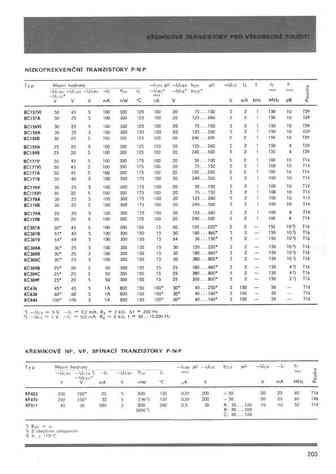
bc635 bc636 bc637 bc638 bc639 bc640.pdf
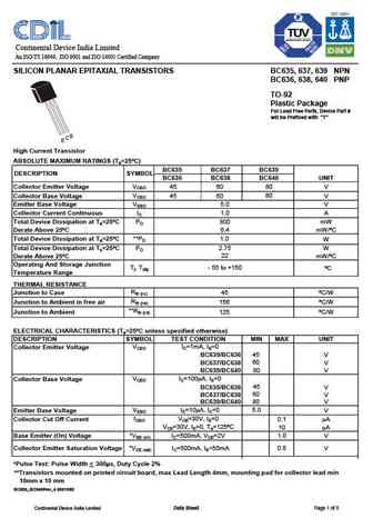
Continental Device India Limited An ISO/TS 16949, ISO 9001 and ISO 14001 Certified Company SILICON PLANAR EPITAXIAL TRANSISTORS BC635, 637, 639 NPN BC636, 638, 640 PNP TO-92 Plastic Package For Lead Free Parts, Device Part # will be Prefixed with "T" B C E High Current Transistor ABSOLUTE MAXIMUM RATINGS (Ta=25 C) BC635 BC637 BC639 DESCRIPTION SYMBOL BC636 BC638 BC640 UNIT VCE
cnl635 cpl636 cnl637 cpl638 cnl639 cpl640.pdf
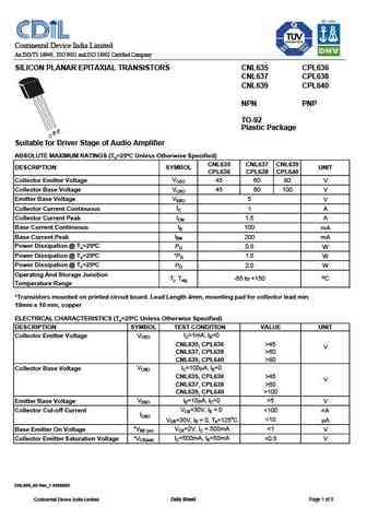
Continental Device India Limited An ISO/TS 16949, ISO 9001 and ISO 14001 Certified Company SILICON PLANAR EPITAXIAL TRANSISTORS CNL635 CPL636 CNL637 CPL638 CNL639 CPL640 NPN PNP TO-92 Plastic Package E CB Suitable for Driver Stage of Audio Amplifier ABSOLUTE MAXIMUM RATINGS (Ta=25 C Unless Otherwise Specified) CNL635 CNL637 CNL639 DESCRIPTION SYMBOL UNIT CPL636 CPL638 CPL640 Col
cvl639 cvl640.pdf
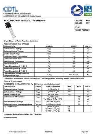
Continental Device India Limited An ISO/TS 16949, ISO 9001 and ISO 14001 Certified Company NPN SILICON PLANAR EPITAXIAL TRANSISTORS CVL639 PNP CVL640 TO-92 Plastic Package E CB Driver Stages of Audio Amplifier Application ABSOLUTE MAXIMUM RATINGS DESCRIPTION SYMBOL VALUE UNITS VCBO Collector Base Voltage 150 V VCEO Collector Emitter Voltage 135 V VEBO Emitter Base Voltage 5.0
irff640.pdf
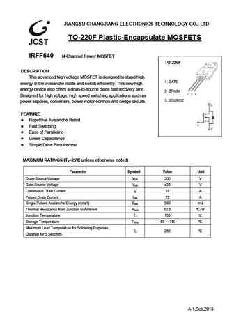
JIANGSU CHANGJIANG ELECTRONICS TECHNOLOGY CO., LTD TO-220F Plastic-Encapsulate MOSFETS IRFF640 N-Channel Power MOSFET TO-220F DESCRIPTION This advanced high voltage MOSFET is designed to stand high 1. GATE energy in the avalanche mode and switch efficiently. This new high energy device also offers a drain-to-source diode fast recovery time. 2. DRAIN Designed for high volta
bc636 bc638 bc640.pdf
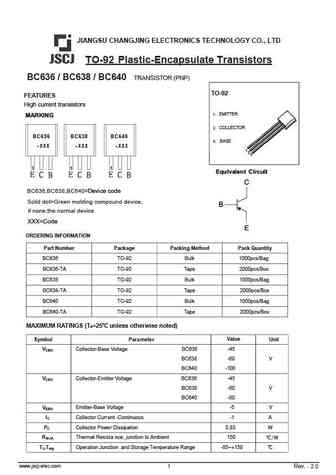
JIANGSU CHANGJING ELECTRONICS TECHNOLOGY CO., LTD TO-92 Plastic-Encapsulate Transistors BC636 / BC638 / BC640 TRANSISTOR (PNP) TO-92 FEATURES High current transistors 1. EMITTER 2. COLLECTOR BC636 BC638 BC640 3. BASE XXX XXX XXX 1 1 1 Equivalent Circuit BC636,BC638,BC640=Device code Solid dot=Green molding compound device, if none,the normal device XXX=Co
2sa1640.pdf
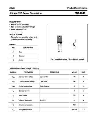
JMnic Product Specification Silicon PNP Power Transistors 2SA1640 DESCRIPTION With TO-220F package Low collector saturation voltage Good linearity of hFE APPLICATIONS For switching regulator ,driver and power amplifier applications PINNING PIN DESCRIPTION 1 Base 2 Collector Fig.1 simplified outline (TO-220F) and symbol 3 Emitter Absolute maximum ratings (Ta=2
2sb1640.pdf
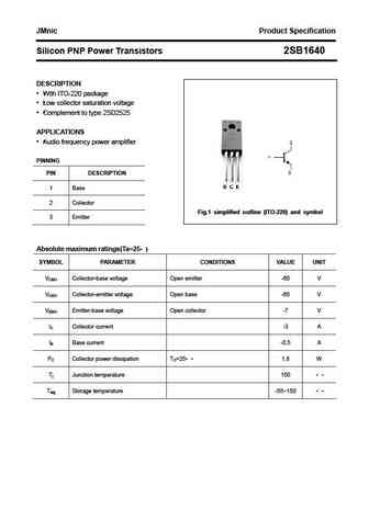
JMnic Product Specification Silicon PNP Power Transistors 2SB1640 DESCRIPTION With ITO-220 package Low collector saturation voltage Complement to type 2SD2525 APPLICATIONS Audio frequency power amplifier PINNING PIN DESCRIPTION 1 Base 2 Collector Fig.1 simplified outline (ITO-220) and symbol 3 Emitter Absolute maximum ratings(Ta=25 ) SYMBOL PARAMETER CONDITI
ktc3640v.pdf
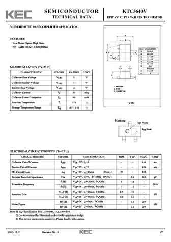
SEMICONDUCTOR KTC3640V TECHNICAL DATA EPITAXIAL PLANAR NPN TRANSISTOR VHF/UHF/WIDE BAND AMPLIFIER APPLICATON. E FEATURES B Low Noise Figure, High Gain. NF=1.4dB, S21e 2=9.0dB(2GHz) DIM MILLIMETERS 2 _ A 1.2 +0.05 _ B 0.8 +0.05 1 3 _ C 0.5 + 0.05 _ D 0.3 + 0.05 _ E 1.2 + 0.05 _ G 0.8 0.05 + H 0.40 P P MAXIMUM RATING (Ta=25 ) _ J 0.12 + 0.05 _ K 0.2 + 0.05 CHARACTE
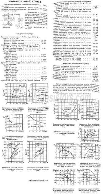
cepf640 cebf640 ceff640.pdf
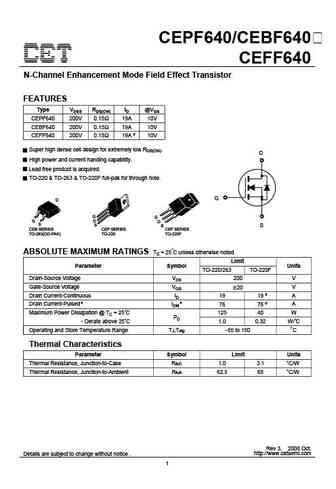
CEPF640/CEBF640 CEFF640 N-Channel Enhancement Mode Field Effect Transistor FEATURES Type VDSS RDS(ON) ID @VGS CEPF640 200V 0.15 19A 10V CEBF640 200V 0.15 19A 10V CEFF640 200V 0.15 19A d 10V Super high dense cell design for extremely low RDS(ON). D High power and current handing capability. Lead free product is acquired. TO-220 & TO-263 & TO-220F full-pak for through hole.
ceuf640 cedf640.pdf
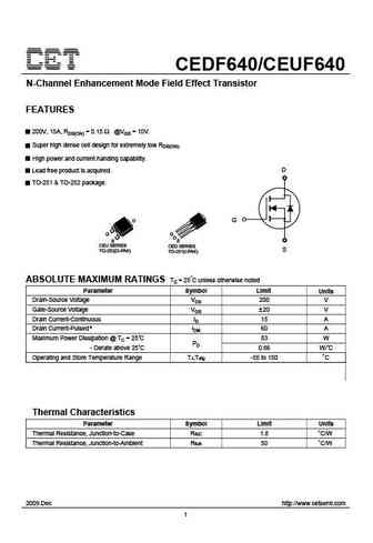
CEDF640/CEUF640 N-Channel Enhancement Mode Field Effect Transistor FEATURES 200V, 15A, RDS(ON) = 0.15 @VGS = 10V. Super high dense cell design for extremely low RDS(ON). High power and current handing capability. D Lead free product is acquired. TO-251 & TO-252 package. D G G S CEU SERIES CED SERIES S TO-252(D-PAK) TO-251(I-PAK) ABSOLUTE MAXIMUM RATINGS Tc = 25 C unless oth
bc636 bc638 bc640.pdf
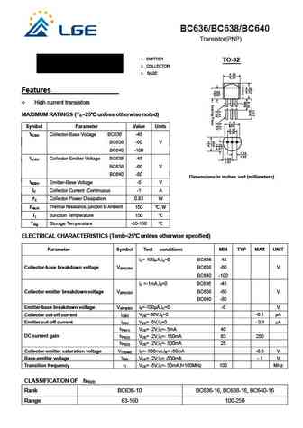
BC636/BC638/BC640 Transistor(PNP) 1. EMITTER TO-92 2. COLLECTOR 3. BASE Features High current transistors MAXIMUM RATINGS (TA=25 unless otherwise noted) Symbol Parameter Value Units VCBO Collector-Base Voltage BC636 -45 BC638 -60 V BC640 -100 VCEO Collector-Emitter Voltage BC636 -45 BC638 -60 V BC640 -80 Dimensions in inches and (millimeters) VEBO Emitter-
irf640.pdf
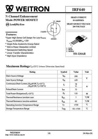
IRF640 N-Channel Enhancement DRAIN CURRENT Mode POWER MOSFET 18 AMPERES 3 DRAIN DRAIN SOURCE VOLTAGE P b Lead(Pb)-Free 200 VOLTAGE 1 GATE Features 2 *Super High Dense Cell Design For Low RDS(ON) SOURCE RDS(ON)
aoi66406.pdf
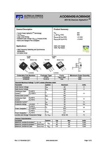
AOD66406/AOI66406 TM 40V N-Channel AlphaSGT General Description Product Summary VDS 40V Trench Power AlphaSGTTM technology ID (at VGS=10V) 60A Low RDS(ON) Logic Level Driving RDS(ON) (at VGS=10V)
aons66402t.pdf

AONS66402T TM 40V N-Channel AlphaSGT General Description Product Summary VDS 40V Trench Power MOSFET - AlphaSGTTM technology ID (at VGS=10V) 224A Low RDS(ON) Logic Level Gate Drive RDS(ON) (at VGS=10V)
ao6403.pdf
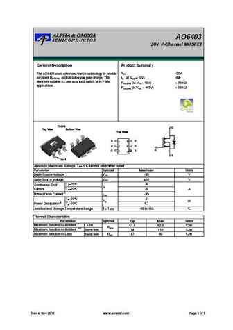
AO6403 30V P-Channel MOSFET General Description Product Summary VDS -30V The AO6403 uses advanced trench technology to provide excellent RDS(ON), and ultra-low low gate charge. This ID (at VGS=-10V) -6A device is suitable for use as a load switch or in PWM RDS(ON) (at VGS=-10V)
ao6405.pdf
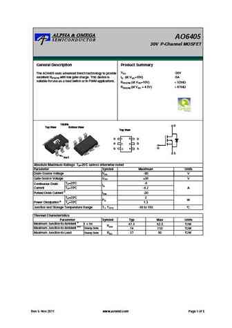
AO6405 30V P-Channel MOSFET General Description Product Summary VDS -30V The AO6405 uses advanced trench technology to provide excellent RDS(ON) with low gate charge. This device is ID (at VGS=10V) -5A suitable for use as a load switch or in PWM applications. RDS(ON) (at VGS=10V)
ao6409a.pdf
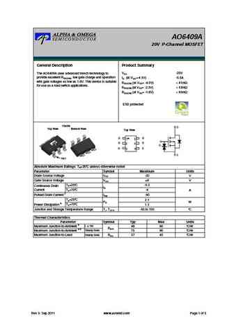
AO6409A 20V P-Channel MOSFET General Description Product Summary VDS -20V The AO6409A uses advanced trench technology to provide excellent RDS(ON), low gate charge and operation ID (at VGS=-4.5V) -5.5A with gate voltages as low as 1.8V. This device is suitable RDS(ON) (at VGS= -4.5V)
aons66407.pdf
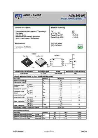
AONS66407 TM 40V N-Channel AlphaSGT General Description Product Summary VDS 40V Trench Power MOSFET - AlphaSGTTM technology ID (at VGS=10V) 370A Low RDS(ON) Low Gate Charge RDS(ON) (at VGS=10V)
ao6402.pdf
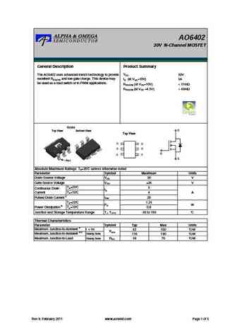
AO6402 30V N-Channel MOSFET General Description Product Summary VDS 30V The AO6402 uses advanced trench technology to provide excellent RDS(ON) and low gate charge. This device may ID (at VGS=10V) 5A be used as a load switch or in PWM applications. RDS(ON) (at VGS=10V)
ao6401.pdf
AO6401 30V P-Channel MOSFET General Description Product Summary VDS -30V The AO6401 uses advanced trench technology to provide excellent RDS(ON), low gate charge and operation with gate ID (at VGS=-10V) -5A voltages as low as 2.5V. This device is suitable for use as RDS(ON) (at VGS=-10V)
ao6408.pdf
AO6408 20V N-Channel MOSFET General Description Features The AO6408 uses advanced trench technology to VDS (V) = 20V provide excellent RDS(ON) and low gate charge. It offers ID = 8.8A (VGS = 10V) operation over a wide gate drive range from 1.8V to RDS(ON)
ao6404.pdf
AO6404 20V N-Channel MOSFET General Description Product Summary The AO6404 uses advanced trench technology to VDS (V) = 20V provide excellent RDS(ON), low gate charge and ID = 8.6A (VGS = 10V) operation with gate voltages as low as 1.8V while RDS(ON)
ao6400.pdf
AO6400 30V N-Channel MOSFET General Description Product Summary VDS 30V The AO6400 uses advanced trench technology to provide excellent RDS(ON), low gate charge and operation with gate ID (at VGS=10V) 6.9A voltages as low as 2.5V. This device is suitable for use as RDS(ON) (at VGS=10V)
ao6409.pdf
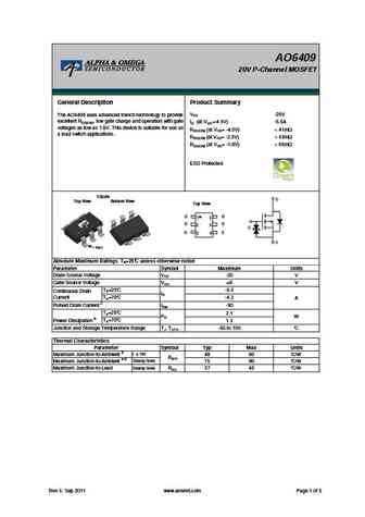
AO6409 20V P-Channel MOSFET General Description Product Summary VDS -20V The AO6409 uses advanced trench technology to provide excellent RDS(ON), low gate charge and operation with gate ID (at VGS=-4.5V) -5.5A voltages as low as 1.8V. This device is suitable for use as RDS(ON) (at VGS= -4.5V)
aons66408.pdf
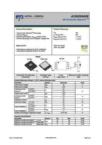
AONS66408 TM 40V N-Channel AlphaSGT General Description Product Summary VDS 40V Trench Power AlphaSGTTM technology ID (at VGS=10V) 85A Very Low RDS(ON) Excellent gate charge x RDS(ON) product (FOM) RDS(ON) (at VGS=10V)
aon6404.pdf
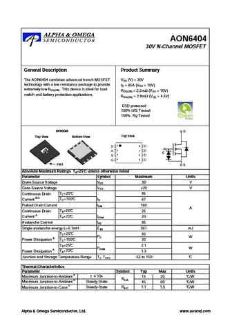
AON6404 30V N-Channel MOSFET General Description Product Summary The AON6404 combines advanced trench MOSFET VDS (V) = 30V technology with a low resistance package to provide ID = 85A (VGS = 10V) extremely low RDS(ON). This device is ideal for load RDS(ON)
aon6403.pdf
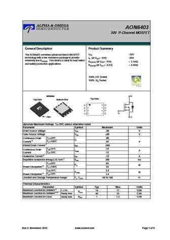
AON6403 30V P-Channel MOSFET General Description Product Summary VDS -30V The AON6403 combines advanced trench MOSFET technology with a low resistance package to provide ID (at VGS= -10V) -85A extremely low RDS(ON). This device is ideal for load switch RDS(ON) (at VGS= -10V)
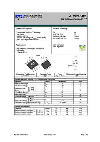
aon6400.pdf
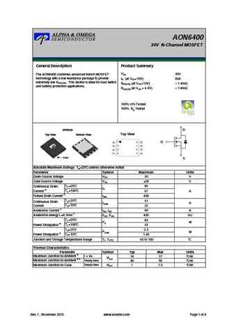
AON6400 30V N-Channel MOSFET General Description Product Summary VDS 30V The AON6400 combines advanced trench MOSFET technology with a low resistance package to provide ID (at VGS=10V) 85A extremely low RDS(ON). This device is ideal for load switch RDS(ON) (at VGS=10V)
aotl66401.pdf
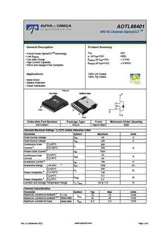
AOTL66401 TM 40V N-Channel AlphaSGT General Description Product Summary VDS 40V Trench Power AlphaSGTTM technology ID (at VGS=10V) 400A Low RDS(ON) Low Gate Charge RDS(ON) (at VGS=10V)
aod66406.pdf

AOD66406/AOI66406 TM 40V N-Channel AlphaSGT General Description Product Summary VDS 40V Trench Power AlphaSGTTM technology ID (at VGS=10V) 60A Low RDS(ON) Logic Level Driving RDS(ON) (at VGS=10V)
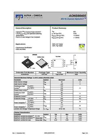
aon6407.pdf
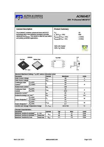
AON6407 30V P-Channel MOSFET General Description Product Summary VDS The AON6407 combines advanced trench MOSFET -30 technology with a low resistance package to provide ID (at VGS= -10V) -85A extremely low RDS(ON). This device is ideal for load switch RDS(ON) (at VGS= -10V)
aons66402.pdf

AONS66402 TM 40V N-Channel AlphaSGT General Description Product Summary VDS 40V Trench Power AlphaSGTTM technology ID (at VGS=10V) 85A Low RDS(ON) Logic Level Gate Drive RDS(ON) (at VGS=10V)
aod66406 aoi66406.pdf
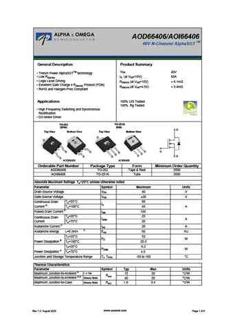
AOD66406/AOI66406 TM 40V N-Channel AlphaSGT General Description Product Summary VDS 40V Trench Power AlphaSGTTM technology ID (at VGS=10V) 60A Low RDS(ON) Logic Level Driving RDS(ON) (at VGS=10V)
aon6404a.pdf
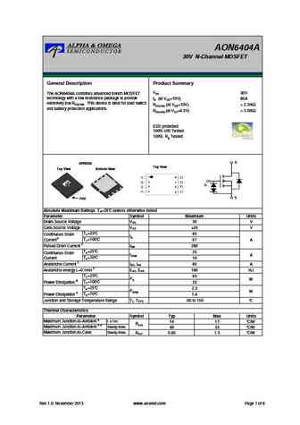
AON6404A 30V N-Channel MOSFET General Description Product Summary VDS 30V The AON6404A combines advanced trench MOSFET technology with a low resistance package to provide ID (at VGS=10V) 85A extremely low RDS(ON). This device is ideal for load switch RDS(ON) (at VGS=10V)
aons66405t.pdf
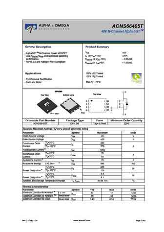
AONS66405T TM 40V N-Channel AlphaSGT General Description Product Summary VDS 40V AlphaSGTTM N-Channel Power MOSFET ID (at VGS=10V) 385A Low RDS(ON)*QOSS and optimised switching performance. RDS(ON) (at VGS=10V)
aon6406.pdf
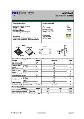
AON6406 30V N-Channel MOSFET General Description Product Summary VDS 30V Latest Trench Power LV technology Very Low RDS(on) at 4.5VGS ID (at VGS=10V) 170A Low Gate Charge RDS(ON) (at VGS=10V)
ao6402a.pdf
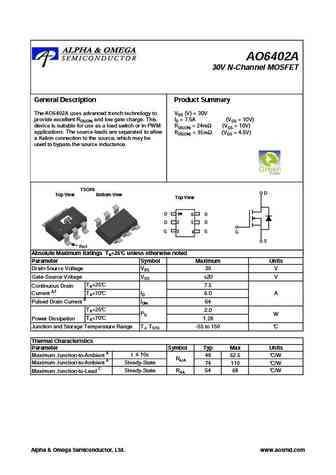
AO6402A 30V N-Channel MOSFET General Description Product Summary The AO6402A uses advanced trench technology to VDS (V) = 30V provide excellent RDS(ON) and low gate charge. This ID = 7.5A (VGS = 10V) device is suitable for use as a load switch or in PWM RDS(ON)
aon6405.pdf
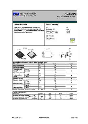
AON6405 30V P-Channel MOSFET General Description Product Summary VDS The AON6405 combines advanced trench MOSFET -30 technology with a low resistance package to provide ID (at VGS= -10V) -30A extremely low RDS(ON). This device is ideal for load switch RDS(ON) (at VGS= -10V)
ao6401a.pdf
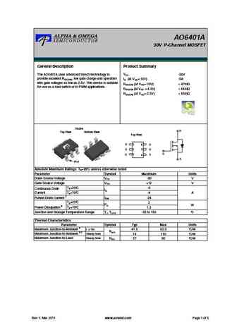
AO6401A 30V P-Channel MOSFET General Description Product Summary VDS -30V The AO6401A uses advanced trench technology to provide excellent RDS(ON), low gate charge and operation ID (at VGS=-10V) -5A with gate voltages as low as 2.5V. This device is suitable RDS(ON) (at VGS=-10V)
aons66406.pdf
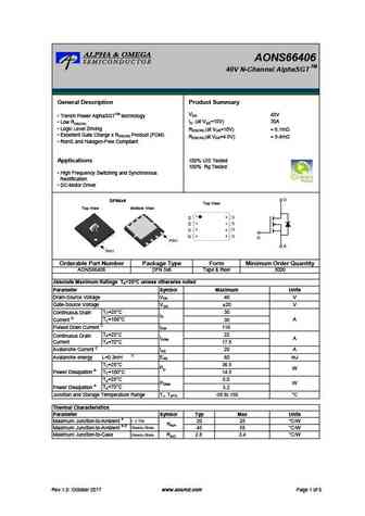
AONS66406 TM 40V N-Channel AlphaSGT General Description Product Summary VDS 40V Trench Power AlphaSGTTM technology ID (at VGS=10V) 30A Low RDS(ON) Logic Level Driving RDS(ON) (at VGS=10V)
aon6408.pdf
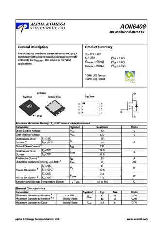
AON6408 30V N-Channel MOSFET General Description Product Summary The AON6408 combines advanced trench MOSFET VDS (V) = 30V technology with a low resistance package to provide ID = 25A (VGS = 10V) extremely low RDS(ON). This device is for PWM RDS(ON)
aonr66406.pdf
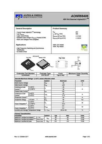
AONR66406 TM 40V N-Channel AlphaSGT General Description Product Summary VDS 40V Trench Power AlphaSGTTM technology ID (at VGS=10V) 30A Low RDS(ON) Logic Level Driving RDS(ON) (at VGS=10V)
am7640n.pdf
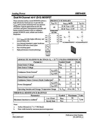
Analog Power AM7640N Dual N-Channel 40-V (D-S) MOSFET These miniature surface mount MOSFETs utilize a PRODUCT SUMMARY high cell density trench process to provide low VDS (V) rDS(on) m( ) ID (A) rDS(on) and to ensure minimal power loss and heat 35 @ V = 10V 7.0 GS dissipation. Typical applications are DC-DC 40 converters and power management in portable and 46 @ V = 4.5V 6.1 GS
afp6405s.pdf
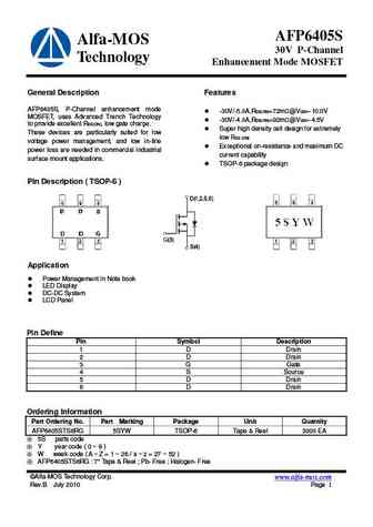
AFP6405S Alfa-MOS 30V P-Channel Technology Enhancement Mode MOSFET General Description Features AFP6405S, P-Channel enhancement mode -30V/-5.0A,RDS(ON)=72m @VGS=-10.0V MOSFET, uses Advanced Trench Technology -30V/-4.0A,RDS(ON)=92m @VGS=-4.5V to provide excellent RDS(ON), low gate charge. Super high density cell design for extremely These devices are particularly s
afp6405ws.pdf
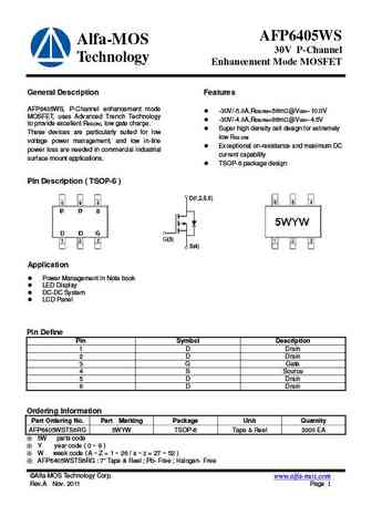
AFP6405WS Alfa-MOS 30V P-Channel Technology Enhancement Mode MOSFET General Description Features AFP6405WS, P-Channel enhancement mode -30V/-5.0A,RDS(ON)=56m @VGS=-10.0V MOSFET, uses Advanced Trench Technology -30V/-4.0A,RDS(ON)=86m @VGS=-4.5V to provide excellent RDS(ON), low gate charge. Super high density cell design for extremely These devices are particularly
irlml6401.pdf
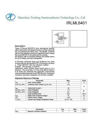
Shenzhen Tuofeng Semiconductor Technology Co., Ltd IRLML6401 G 1 3 D S 2 Description These P-Channel MOSFETs from International Rectifier utilize advanced processing techniques to achieve extremely low on-resistance per silicon area. This benefit, combined with the fast switching speed and ruggedized device design that power MOSFETs are well known for, provides the designer with an
irlml6402.pdf
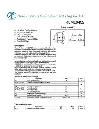
Shenzhen Tuofeng Semiconductor Technology Co., Ltd IRLML6402 Power MOSFET l Ultra Low On-Resistance D l P-Channel MOSFET l SOT-23 Footprint VDSS = -20V l Low Profile (
jcs640s jcs640c jcs640f.pdf
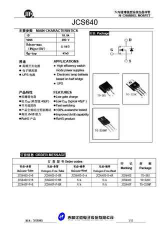
N N- CHANNEL MOSFET R JCS640 MAIN CHARACTERISTICS Package ID 18.0A VDSS 200 V Rdson-max 0.18 @Vgs=10V Qg-typ 47nC APPLICATIONS High efficiency switch mode power supplies Electronic lamp ballasts UPS based on half bridge
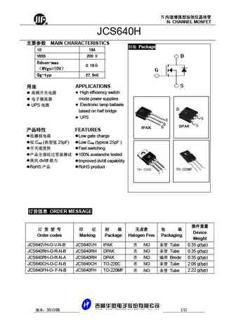
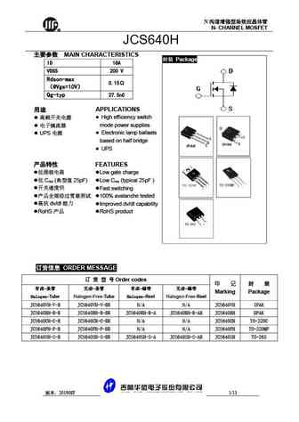
bta1640f3.pdf
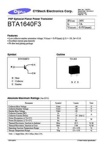
Spec. No. C657F3 Issued Date 2010.09.21 CYStech Electronics Corp. Revised Date Page No. 1/6 PNP Epitaxial Planar Power Transistor BVCEO -30V IC -7A BTA1640F3 VCE(SAT) -0.4V(max) Features Low collector-emitter saturation voltage, VCE(sat) = -0.4V(max) @ IC = -3A, IB=-0.1A Excellent current gain linearity Pb-free lead plating package Symbol Outline
bta1640t3.pdf
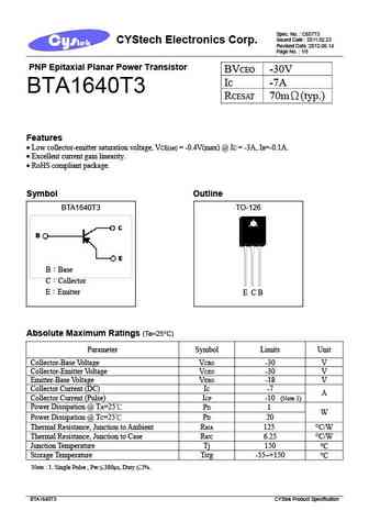
Spec. No. C657T3 Issued Date 2011.02.23 CYStech Electronics Corp. Revised Date 2012.06.14 Page No. 1/5 PNP Epitaxial Planar Power Transistor BVCEO -30V IC -7A BTA1640T3 RCESAT 70m (typ.) Features Low collector-emitter saturation voltage, VCE(sat) = -0.4V(max) @ IC = -3A, IB=-0.1A. Excellent current gain linearity. RoHS compliant package. Symbol Outl
bta1640fp.pdf
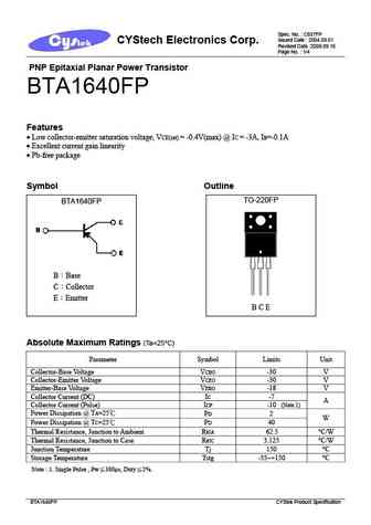
Spec. No. C657FP Issued Date 2004.09.01 CYStech Electronics Corp. Revised Date 2009.09.16 Page No. 1/4 PNP Epitaxial Planar Power Transistor BTA1640FP Features Low collector-emitter saturation voltage, VCE(sat) = -0.4V(max) @ IC = -3A, IB=-0.1A Excellent current gain linearity Pb-free package Symbol Outline TO-220FP BTA1640FP B Base C Collecto
bta1640j3.pdf
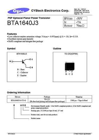
Spec. No. C657J3 Issued Date 2007.04.04 CYStech Electronics Corp. Revised Date 2014.05.23 Page No. 1/6 PNP Epitaxial Planar Power Transistor BVCEO -50V IC -7A BTA1640J3 RCESAT 70m Features Low collector-emitter saturation voltage, VCE(sat) = -0.4V(max) @ IC = -3A, IB=-0.15A Excellent current gain linearity RoHS compliant and halogen-free package Sy
bta1640i3.pdf
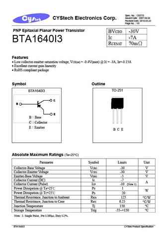
Spec. No. C657I3 Issued Date 2007.04.04 CYStech Electronics Corp. Revised Date 2010.03.23 Page No. 1/5 PNP Epitaxial Planar Power Transistor BVCEO -30V IC -7A BTA1640I3 RCESAT 70m Features Low collector-emitter saturation voltage, VCE(sat) = -0.4V(max) @ IC = -3A, IB=-0.15A Excellent current gain linearity RoHS compliant package Symbol Outline TO
mtp6405n6.pdf
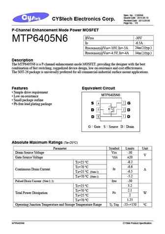
Spec. No. C386N6 Issued Date 2013.08.19 CYStech Electronics Corp. Revised Date 2013.09.06 Page No. 1/9 P-Channel Enhancement Mode Power MOSFET BVDSS -30V MTP6405N6 ID -6.5A 24m (typ.) RDSON(MAX)@VGS=-10V, ID=-5A 34m (typ.) RDSON(MAX)@VGS=-4.5V, ID=-4A Description The MTP6405N6 is a P-channel enhancement-mode MOSFET, providing the designer with the best combi
sts6409.pdf
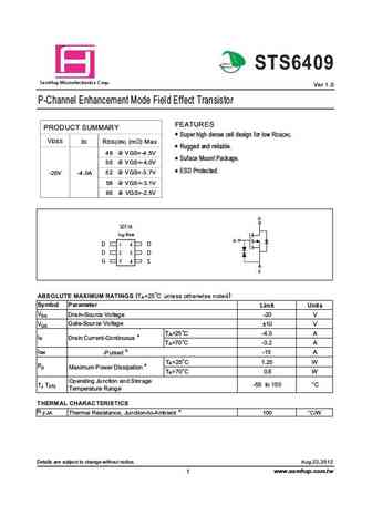
re r r P Pr Pr Pro STS6409 a S mHop Microelectronics C orp. Ver 1.0 P-Channel Enhancement Mode Field Effect Transistor FEATURES PRODUCT SUMMARY Super high dense cell design for low RDS(ON). VDSS ID RDS(ON) (m ) Max Rugged and reliable. 49 @ VGS=-4.5V Suface Mount Package. 50 @ VGS=-4.0V ESD Protected. 52 @ VGS=-3.7V -20V -4.0A 58 @ VGS=-3.1V 65 @ VGS=-2.5V D SOT 26 T
p6402fmg.pdf
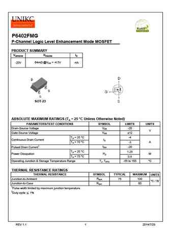
P6402FMG P-Channel Logic Level Enhancement Mode MOSFET PRODUCT SUMMARY V(BR)DSS RDS(ON) ID 64m @VGS = -4.5V -20V -4A SOT-23 ABSOLUTE MAXIMUM RATINGS (TA = 25 C Unless Otherwise Noted) PARAMETERS/TEST CONDITIONS SYMBOL LIMITS UNITS VDS Drain-Source Voltage -20 V VGS Gate-Source Voltage 12 TA = 25 C -4 ID Continuous Drain Current TA = 70 A C -3 IDM -20 Pulse
p6403fmg.pdf
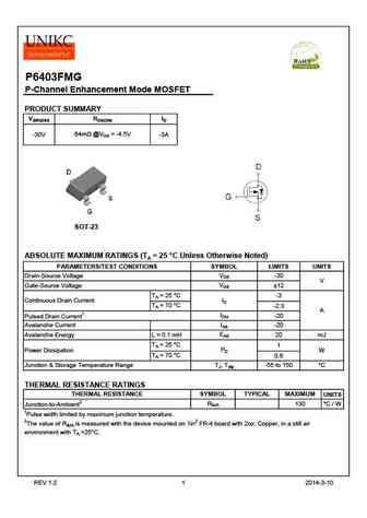
P6403FMG P-Channel Enhancement Mode MOSFET PRODUCT SUMMARY V(BR)DSS RDS(ON) ID 64m @VGS = -4.5V -30V -3A SOT-23 ABSOLUTE MAXIMUM RATINGS (TA = 25 C Unless Otherwise Noted) PARAMETERS/TEST CONDITIONS SYMBOL LIMITS UNITS VDS Drain-Source Voltage -30 V VGS Gate-Source Voltage 12 TA = 25 C -3 ID Continuous Drain Current TA = 70 C -2.3 A IDM -20 Pulsed Drain C
ssf6401.pdf
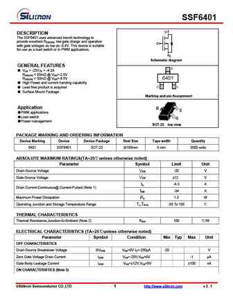
SSF6401 D DESCRIPTION The SSF6401 uses advanced trench technology to provide excellent RDS(ON), low gate charge and operation G with gate voltages as low as -0.4V. This device is suitable for use as a load switch or in PWM applications. S Schematic diagram GENERAL FEATURES VDS = -20V,ID = -4.3A RDS(ON)
brd640.pdf
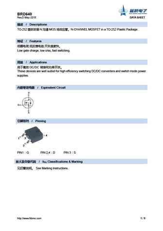
BRD640 Rev.D May.-2016 DATA SHEET / Descriptions TO-252 N MOS N-CHANNEL MOSFET in a TO-252 Plastic Package. / Features , , Low gate charge, low crss, fast switching. / Applications DC/DC These devices are well suited for high efficiency swi
vti640.pdf
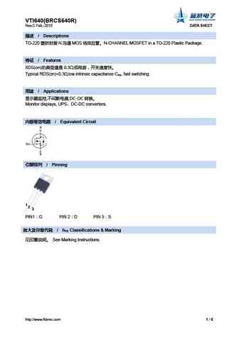
VTI640(BRCS640R) Rev.C Feb.-2015 DATA SHEET / Descriptions TO-220 N MOS N-CHANNEL MOSFET in a TO-220 Plastic Package. / Features RDS(on) 0.3 , Typical RDS(on)=0.3 ,low intrinsic capacitance Ciss, fast switching. / Applications , ,DC-DC
irf640.pdf
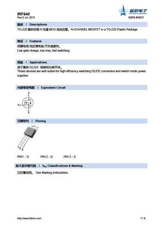
IRF640 Rev.G Jul.-2018 DATA SHEET / Descriptions TO-220 N MOS N-CHANNEL MOSFET in a TO-220 Plastic Package. / Features , , Low gate charge, low crss, fast switching. / Applications DC/DC These devices are well suited for high efficiency swi
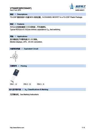
irf640h.pdf
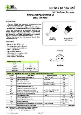
RoHS IRF640 Series RoHS SEMICONDUCTOR Nell High Power Products N-Channel Power MOSFET (18A, 200Volts) DESCRIPTION The Nell IRF640 are N-channel enhancement mode silicon gate power field effect transistors. D D They are designed, tested and guaranteed to withstand level of energy in breakdown avalanche made of operation. They are designed as an extremely efficient and relia
hfp640.pdf
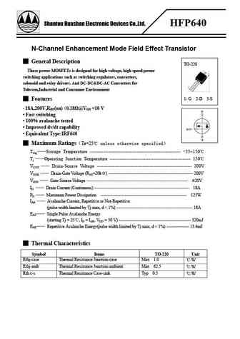
Shantou Huashan Electronic Devices Co.,Ltd. HFP640 N-Channel Enhancement Mode Field Effect Transistor General Description TO-220 These power MOSFETs is designed for high voltage, high speed power switching applications such as switching regulators, converters, solenoid and relay drivers. And DC-DC&DC-AC Converters for Telecom,Industrial and Consumer Environment 1- G 2-D 3
hff640.pdf
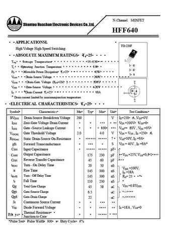
N-Channel MOSFET Shantou Huashan Electronic Devices Co.,Ltd. HFF640 APPLICATIONSL TO-220F High Voltage High-Speed Switching. ABSOLUTE MAXIMUM RATINGS Ta=25 1 Tstg Storage Temperature -55 150 1 G Tj Operating Junction Temperature 150 2 D PD Allowable Power Dissipatio
cs640 a0h.pdf

Silicon N-Channel Power MOSFET R CS640 A0H General Description VDSS 200 V CS640 A0H, the silicon N-channel Enhanced ID 18 A PD(TC=25 ) 156 W VDMOSFETs, is obtained by the self-aligned planar Technology RDS(ON)Typ 0.12 which reduce the conduction loss, improve switching performance and enhance the avalanche energy. The transistor can be used in various power
cs640 a8h.pdf
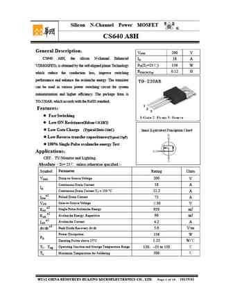
Silicon N-Channel Power MOSFET R CS640 A8H General Description VDSS 200 V CS640 A8H, the silicon N-channel Enhanced ID 18 A PD(TC=25 ) 156 W VDMOSFETs, is obtained by the self-aligned planar Technology RDS(ON)Typ 0.12 which reduce the conduction loss, improve switching performance and enhance the avalanche energy. The transistor can be used in various power s
cs640f a9h.pdf
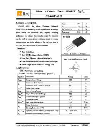
Silicon N-Channel Power MOSFET R CS640F A9H General Description VDSS 200 V CS640F A9H, the silicon N-channel Enhanced ID 18 A PD(TC=25 ) 55 W VDMOSFETs, is obtained by the self-aligned planar Technology RDS(ON)Typ 0.12 which reduce the conduction loss, improve switching performance and enhance the avalanche energy. The transistor can be used in various pow
cs640.pdf
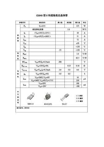
CS640 N PD TC=25 125 W 1.0 W/ ID VGS=10V,TC=25 18 A ID VGS=10V,TC=100 11 A IDM 72 A VGS 20 V Tjm +150 Tstg -55 +150 RthJC 1.0 /W RthJA 62.5 /W BVDSS VGS=0V,ID=0.25mA 200 V RDS on VGS=10
cs9640.pdf

CS9640 P PD TC=25 125 W 1.0 W/ ID VGS=-10V,TC=25 -11 A ID VGS=-10V,TC=100 -7 A IDM -44 A VGS 20 V Tjm +150 Tstg -55 +150 RthJC 1.0 /W RthJA 62.5 /W BVDSS VGS=0V,ID=-0.25mA -200 V RDS on VGS=-10V,ID=
irlml6401.pdf
Product specification IRLML6401PbF HEXFET Power MOSFET l Ultra Low On-Resistance l P-Channel MOSFET l SOT-23 Footprint l Low Profile (
krlml6402.pdf
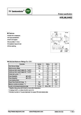
SMD Type SMD Type SMD Type SMD Type SMD Type SMD Type SMD Type SMD Type SMD Type SMD Type SMD Type SMD Type SMD Type SMD Type SMD Type SMD Type SMD Type SMD Type SMD Type SMD Type IC SMD Type IC SMD Type IC SMD Type IC SMD Type IC SMD Type IC SMD Type IC SMD Type IC SMD Type IC SMD Type IC SMD Type MOSFET SMD Type MOSFE SMD Type MOSFE SMD Type SMD Type SMD Type
irlml6402.pdf
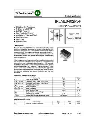
Product specification IRLML6402PbF HEXFET Power MOSFET l Ultra Low On-Resistance l P-Channel MOSFET l SOT-23 Footprint G 1 l Low Profile (
ftk6401.pdf
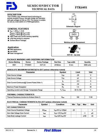
SEMICONDUCTOR FTK6401 TECHNICAL DATA D DESCRIPTION The FTK6401 uses advanced trench technology to provide excellent RDS(ON), low gate charge and operation G with gate voltages as low as 2.5V. This device is suitable for use as a load switch or in PWM applications. S Schematic diagram GENERAL FEATURES VDS = -20V,ID = -4.3A RDS(ON)
ftk640p f.pdf
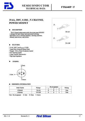
SEMICONDUCTOR FTK640P / F TECHNICAL DATA 19.4A, 200V, 0.18 , N-CHANNEL POWER MOSFET P 1 DESCRIPTION TO-220 The N-Channel enhancement mode silicon gate power MOSFET is designed for high voltage, high speed power switching applications such as switching regulators, switching converters, solenoid, motor drivers, relay drivers. F 1 TO-220F FEATURES * 19.4A, 200V, Low RDS(ON)
ao6403.pdf
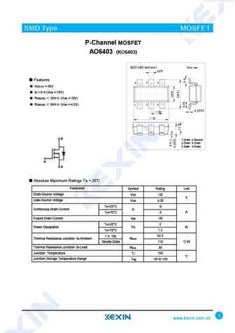
SMD Type MOSFET P-Channel MOSFET AO6403 (KO6403) ( ) SOT-23-6 Unit mm 0.4+0.1 -0.1 Features 6 5 4 VDS (V) =-30V ID =-6 A (VGS =-10V) RDS(ON) 35m (VGS =-10V) RDS(ON) 58m (VGS =-4.5V) 2 3 1 +0.02 0.15 -0.02 +0.01 -0.01 +0.2 -0.1 D D 1 Drain 4 Source 2 Drain 5 Drain 3 Gate 6 Drain G G S S Absolute Maximum Ratings Ta = 25 Par
ao6405.pdf
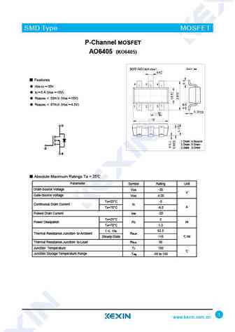
SMD Type MOSFET P-Channel MOSFET AO6405 (KO6405) ( ) SOT-23-6 Unit mm 0.4+0.1 -0.1 Features 6 5 4 VDS (V) =-30V ID =-5 A (VGS =-10V) RDS(ON) 52m (VGS =-10V) RDS(ON) 87m (VGS =-4.5V) 2 3 1 +0.02 0.15 -0.02 +0.01 -0.01 +0.2 -0.1 D D 1 Drain 4 Source 2 Drain 5 Drain 3 Gate 6 Drain G G S S Absolute Maximum Ratings Ta = 25 Pa
2sk3640.pdf
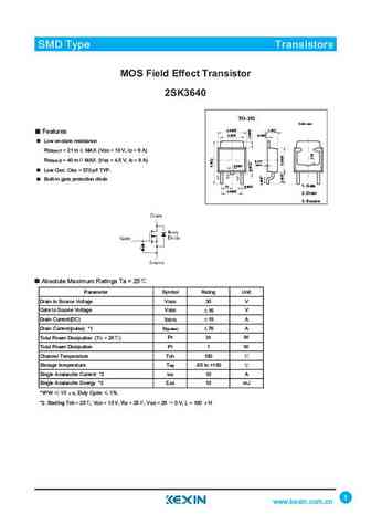
SMD Type IC SMD Type Transistors MOS Field Effect Transistor 2SK3640 TO-252 Unit mm 6.50+0.15 2.30+0.1 -0.15 -0.1 Features +0.2 5.30-0.2 0.50+0.8 -0.7 Low on-state resistance RDS(on)1 =21m MAX. (VGS =10 V, ID =9A) RDS(on)2 =40m MAX. (VGS =4.5 V, ID =9 A) 0.127 0.80+0.1 max -0.1 Low Ciss Ciss = 570 pF TYP. Built-in gate protection diode 1. Gate 2.3 0.60+0.1 -0.1 4.60+0.1
ao6409a.pdf
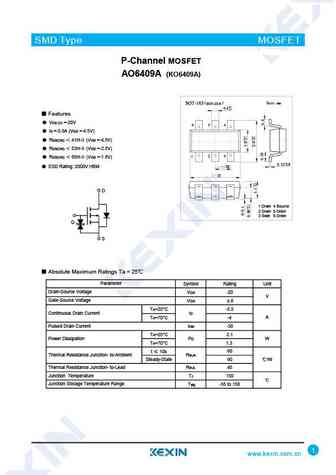
SMD Type MOSFET P-Channel MOSFET AO6409A (KO6409A) ( ) SOT-23-6 Unit mm 0.4+0.1 -0.1 Features VDS (V) =-20V 6 5 4 ID =-5.5A (VGS =-4.5V) RDS(ON) 41m (VGS =-4.5V) RDS(ON) 53m (VGS =-2.5V) 2 3 1 RDS(ON) 65m (VGS =-1.8V) +0.02 0.15 -0.02 +0.01 ESD Rating 2000V HBM -0.01 +0.2 -0.1 D 1 Drain 4 Source 2 Drain 5 Drain 3 Gat
irlml6401.pdf

SMD Type SM MOSFET P-Channel Enhancement MOSFET IRLML6401 KRLML6401) ( SOT-23 Unit mm +0.1 2.9 -0.1 Features +0.1 0.4 -0.1 Ultra low on-resistance. 3 P-Channel MOSFET. Fast switching. 1 2 +0.1 +0.05 0.95 -0.1 0.1 -0.01 +0.1 1.9 -0.1 1.Base 1. Gate 2.Emitter 2. Source 3. Drain 3.collector Absolute Maximum Ratings Ta = 25 Parameter Symbol Ra
ao6402.pdf
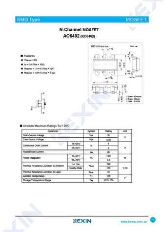
SMD Type MOSFET N-Channel MOSFET AO6402 (KO6402) ( ) SOT-23-6 Unit mm 0.4+0.1 -0.1 Features 6 5 4 VDS (V) = 30V ID = 5 A (VGS = 10V) RDS(ON) 31m (VGS = 10V) 2 3 1 RDS(ON) 43m (VGS = 4.5V) +0.02 0.15 -0.02 +0.01 -0.01 +0.2 -0.1 D 1 Drain 4 Source 2 Drain 5 Drain 3 Gate 6 Drain G S Absolute Maximum Ratings Ta = 25 Parameter S
ao6401.pdf
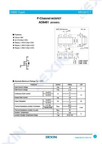
SMD Type MOSFET P-Channel MOSFET AO6401 (KO6401) ( ) SOT-23-6 Unit mm 0.4+0.1 -0.1 Features 6 5 4 VDS (V) =-30V ID =-5 A (VGS =-10V) RDS(ON) 47m (VGS =-10V) RDS(ON) 64m (VGS =-4.5V) 2 3 1 +0.02 0.15 -0.02 RDS(ON) 85m (VGS =-2.5V) +0.01 -0.01 +0.2 -0.1 D D 1 Drain 4 Source 2 Drain 5 Drain 3 Gate 6 Drain G G S S Abso
krf9640s.pdf
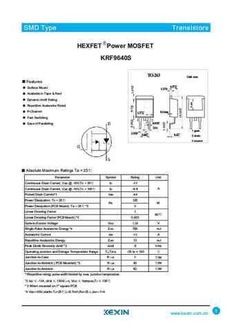
SMD Type IC SMD Type Transistors HEXFET Power MOSFET KRF9640S TO-263 Unit mm Features 4.57+0.2 -0.2 Surface Mount +0.1 1.27-0.1 Available in Tape & Reel Dynamic dv/dt Rating Repetitive Avalanche Rated +0.1 P-Channel 0.1max 1.27-0.1 Fast Switching 0.81+0.1 -0.1 Ease of Paralleling 2.54 1gate 1Gate 2.54+0.2 +0.2 -0.2 +0.1 5.08-0.1 0.4-0.2 2drain 2Drain 3Source sour
irlml6402.pdf
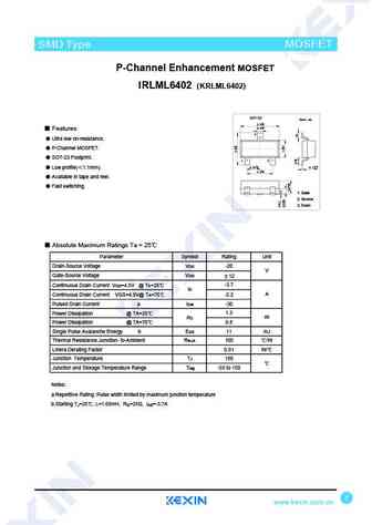
SMD Type MOSFET P-Channel Enhancement MOSFET IRLML6402 ( KRLML6402) SOT-23 Unit mm +0.1 2.9 -0.1 +0.1 0.4 -0.1 Features 3 Ultra low on-resistance. P-Channel MOSFET. SOT-23 Footprint. 1 2 +0.1 +0.05 0.95 -0.1 Low profile( 1.1mm). 0.1 -0.01 +0.1 1.9 -0.1 Available in tape and reel. Fast switching. 1.Base 1. Gate 2.Emitter 2. Source 3
ao6408.pdf
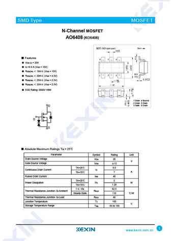
SMD Type MOSFET N-Channel MOSFET AO6408 (KO6408) ( ) SOT-23-6 Unit mm 0.4+0.1 -0.1 Features 6 5 4 VDS (V) = 20V ID =8.8 A (VGS = 10V) RDS(ON) 18m (VGS = 10V) 2 3 1 RDS(ON) 20m (VGS = 4.5V) +0.02 0.15 -0.02 +0.01 RDS(ON) 25m (VGS = 2.5V) -0.01 +0.2 RDS(ON) 32m (VGS = 2.5V) -0.1 ESD Rating 2000V HBM 1 Drain 4
ao6404.pdf
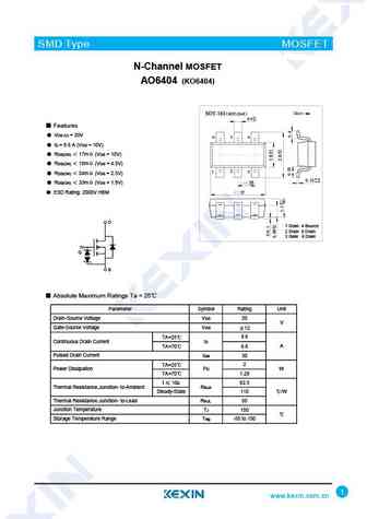
SMD Type MOSFET N-Channel MOSFET AO6404 (KO6404) ( ) SOT-23-6 Unit mm 0.4+0.1 -0.1 Features VDS (V) = 20V 6 5 4 ID = 8.6 A (VGS = 10V) RDS(ON) 17m (VGS = 10V) RDS(ON) 18m (VGS = 4.5V) 2 3 1 RDS(ON) 24m (VGS = 2.5V) +0.02 0.15 -0.02 +0.01 RDS(ON) 33m (VGS = 1.8V) -0.01 +0.2 ESD Rating 2000V HBM -0.1 D 1 Drain
irlml6402-3.pdf
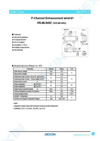
SMD Type MOSFET P-Channel Enhancement MOSFET IRLML6402 ( KRLML6402) SOT-23-3 Unit mm +0.2 2.9 -0.1 +0.1 0.4 -0.1 3 Features Ultra low on-resistance. P-Channel MOSFET. 1 2 SOT-23 Footprint. +0.02 +0.1 0.15 -0.02 0.95-0.1 Low profile( 1.1mm). +0.1 1.9 -0.2 Available in tape and reel. Fast switching. 1.Base 1. Gate 2.Emitter 2. Source
ao6400.pdf
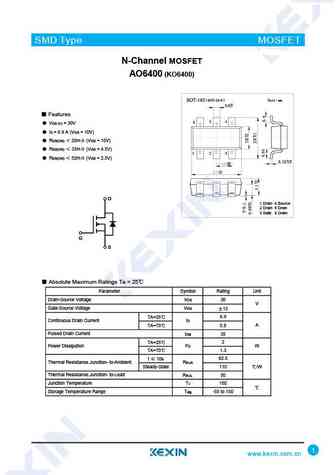
SMD Type MOSFET N-Channel MOSFET AO6400 (KO6400) ( ) SOT-23-6 Unit mm 0.4+0.1 -0.1 Features 6 5 4 VDS (V) = 30V ID = 6.9 A (VGS = 10V) RDS(ON) 28m (VGS = 10V) RDS(ON) 33m (VGS = 4.5V) 2 3 1 RDS(ON) 52m (VGS = 2.5V) +0.02 0.15 -0.02 +0.01 -0.01 +0.2 -0.1 D D 1 Drain 4 Source 2 Drain 5 Drain 3 Gate 6 Drain G G S S
ao6409.pdf

SMD Type MOSFET P-Channel MOSFET AO6409 (KO6409) ( ) SOT-23-6 Unit mm 0.4+0.1 -0.1 Features VDS (V) =-20V 6 5 4 ID =-5.5A (VGS =-4.5V) RDS(ON) 41m (VGS =-4.5V) RDS(ON) 53m (VGS =-2.5V) 2 3 1 RDS(ON) 65m (VGS =-1.8V) +0.02 0.15 -0.02 +0.01 ESD Rating 2000V HBM -0.01 +0.2 -0.1 D 1 Drain 4 Source 2 Drain 5 Drain 3 Gate
irlml6401-3.pdf

SMD Type SM MOSFET P-Channel Enhancement MOSFET IRLML6401 KRLML6401) ( SOT-23-3 Unit mm +0.2 2.9 -0.1 +0.1 0.4 -0.1 Features 3 Ultra low on-resistance. P-Channel MOSFET. Fast switching. 1 2 +0.02 +0.1 0.15 -0.02 0.95-0.1 +0.1 1.9 -0.2 1.Base 1. Gate 2.Emitter 2. Source 3. Drain 3.collector Absolute Maximum Ratings Ta = 25 Parameter Symbol
mch6405.pdf
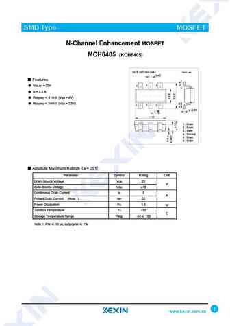
SMD Type MOSFET N-Channel Enhancement MOSFET MCH6405 (KCH6405) ( ) SOT-23-6 Unit mm 0.4+0.1 -0.1 Features 6 5 4 VDS (V) = 20V ID = 5.0 A RDS(ON) 41m (VGS = 4V) RDS(ON) 54m (VGS = 2.5V) 2 3 1 +0.02 0.15 -0.02 +0.01 -0.01 +0.2 -0.1 1 Drain 2 Drain 3 Gate 4 Source 5 Drain 6 Drain Absolute Maximum Ratings Ta = 25 Pa
ao6401-hf ko6401-hf.pdf
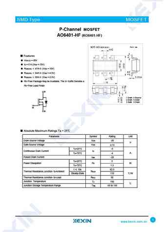
SMD Type MOSFET P-Channel MOSFET AO6401-HF (KO6401-HF) ( ) SOT-23-6 Unit mm 0.4+0.1 -0.1 Features 6 5 4 VDS (V) =-30V ID =-5 A (VGS =-10V) RDS(ON) 47m (VGS =-10V) RDS(ON) 64m (VGS =-4.5V) 2 3 1 +0.02 0.15 -0.02 RDS(ON) 85m (VGS =-2.5V) +0.01 -0.01 Pb-Free Package May be Available. The G-Suffix Denotes a +0.2 -0.1 Pb-Free
ao6402a.pdf
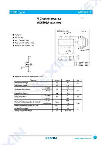
SMD Type MOSFET N-Channel MOSFET AO6402A (KO6402A) ( ) SOT-23-6 Unit mm 0.4+0.1 -0.1 Features VDS (V) = 30V 6 5 4 ID = 7.5 A (VGS = 10V) RDS(ON) 24m (VGS = 10V) RDS(ON) 35m (VGS = 4.5V) 2 3 1 +0.02 0.15 -0.02 +0.01 -0.01 +0.2 -0.1 D 1 Drain 4 Source 2 Drain 5 Drain 3 Gate 6 Drain G S Absolute Maximum Ratings Ta = 25 Parame
ao6401a.pdf
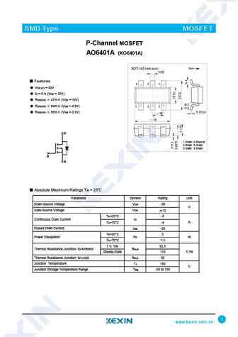
SMD Type MOSFET P-Channel MOSFET AO6401A (KO6401A) ( ) SOT-23-6 Unit mm 0.4+0.1 -0.1 Features 6 5 4 VDS (V) =-30V ID =-5 A (VGS =-10V) RDS(ON) 47m (VGS =-10V) RDS(ON) 64m (VGS =-4.5V) 2 3 1 +0.02 0.15 -0.02 RDS(ON) 85m (VGS =-2.5V) +0.01 -0.01 +0.2 -0.1 D D 1 Drain 4 Source 2 Drain 5 Drain 3 Gate 6 Drain G G S S Ab
irlml6401 krlml6401.pdf
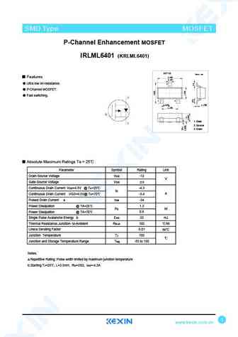
SMD Type SM MOSFET P-Channel Enhancement MOSFET IRLML6401 KRLML6401) ( SOT-23 Unit mm +0.1 2.9 -0.1 Features +0.1 0.4 -0.1 Ultra low on-resistance. 3 P-Channel MOSFET. Fast switching. 1 2 +0.1 +0.05 0.95 -0.1 0.1 -0.01 +0.1 1.9 -0.1 1.Base 1. Gate 2.Emitter 2. Source 3. Drain 3.collector Absolute Maximum Ratings Ta = 25 Parameter Symbol Ra
svd640t svd640d svd640f.pdf
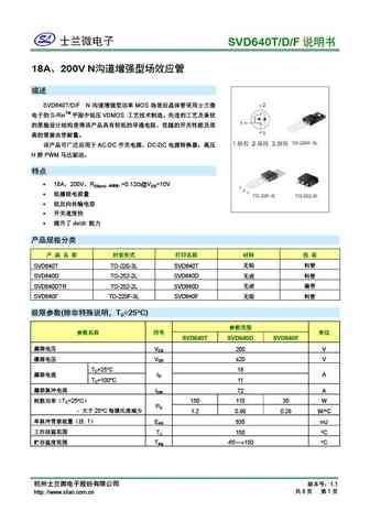
SVD640T/D/F 18A 200V N SVD640T/D/F N MOS S-RinTM VDMOS AC-DC
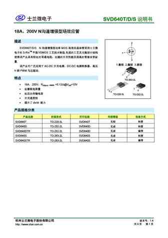
wfp640.pdf
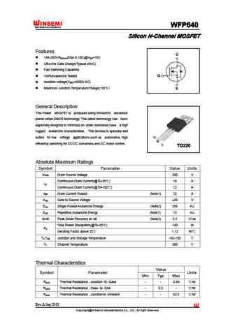
WFP640 WFP640 WFP640 WFP640 Silicon N-Channel MOSFET Silicon N-Channel MOSFET Silicon N-Channel MOSFET Silicon N-Channel MOSFET Features 18A,200V,R (Max 0.18 )@V =10V DS(on) GS Ultra-low Gate Charge(Typical 45nC) Fast Switching Capability 100%Avalanche Tested Isolation voltage(V =4000V AC) ISO Maximum Junction Temperature Range(150 ) General Descript
wff640.pdf
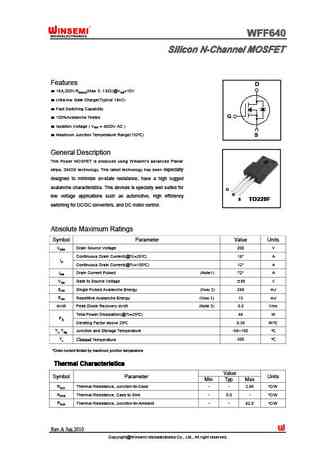
WFF640 WFF640 WFF640 WFF640 Silicon N-Channel MOSFET Silicon N-Channel MOSFET Silicon N-Channel MOSFET Silicon N-Channel MOSFET Features 18A,200V.RDS(on)(Max 0.1 8 )@VGS=10V Ultra-low Gate Charge(Typical 16nC) Fast Switching Capability 100%Avalanche Tested Isolation Voltage ( VISO = 4000V AC ) Maximum Junction Temperature Range(150 ) General Description
sfp640.pdf
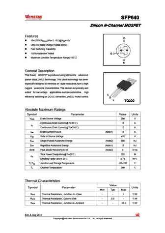
SFP640 SFP640 SFP640 SFP640 Silicon N-Channel MOSFET Silicon N-Channel MOSFET Silicon N-Channel MOSFET Silicon N-Channel MOSFET Features 18A,200V,R (Max 0.18 )@V =10V DS(on) GS Ultra-low Gate Charge(Typical 40nC) Fast Switching Capability 100%Avalanche Tested Maximum Junction Temperature Range(150 ) General Description This Power MOSFET is produced using
pjs6400.pdf
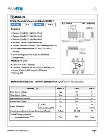
PPJS6400 30V N-Channel Enhancement Mode MOSFET SOT-23 6L-1 Unit inch(mm) Voltage 30 V Current 6.4A Features RDS(ON) , VGS@10V, ID@6.4A
pjs6407.pdf
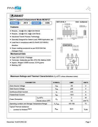
PPJS6407 30V P-Channel Enhancement Mode MOSFET SOT-23 6L-1 Unit inch(mm) Voltage -30 V Current -4.9A Features RDS(ON) , VGS@-10V, ID@-4.9A
pjs6403.pdf
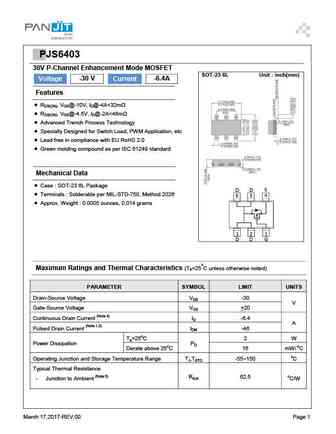
PPJS6403 30V P-Channel Enhancement Mode MOSFET SOT-23 6L Unit inch(mm) Voltage -30 V Current -6.4A Features RDS(ON), VGS@-10V, ID@-4A
pjs6401.pdf

PPJS6401 30V P-Channel Enhancement Mode MOSFET SOT-23 6L-1 Unit inch(mm) Voltage -30 V Current -4.6A Features RDS(ON) , VGS@-10V, ID@-4.6A
pjs6405.pdf

PPJS6405 30V P-Channel Enhancement Mode MOSFET SOT-23 6L-1 Unit inch(mm) Voltage -30 V Current -4.6A Features RDS(ON) , VGS@-10V, ID@-4.6A
pjs6404.pdf
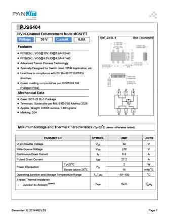
PPJS6404 30V N-Channel Enhancement Mode MOSFET SOT-23 6L-1 Unit inch(mm) Voltage 30 V Current 6.8A Features RDS(ON) , VGS@10V, ID@6.8A
am6401.pdf
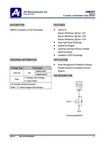
AiT Semiconductor Inc. AM6401 www.ait-ic.com MOSFET P-CHANNEL ENHANCEMENT MODE MOSFET DESCRIPTION FEATURES AM6401 is available in a SOT-26 package. -30V/-5.1A, R = 54m (max.) @ V = -10V DS(ON) GS R = 65m (max.) @ V = -4.5V DS(ON) GS R = 92m (max.) @ V = -2.5V DS(ON) GS Super High Dense Cell Design Reliable and Rugged Lead Free and Green Devices Availabl
blv640.pdf
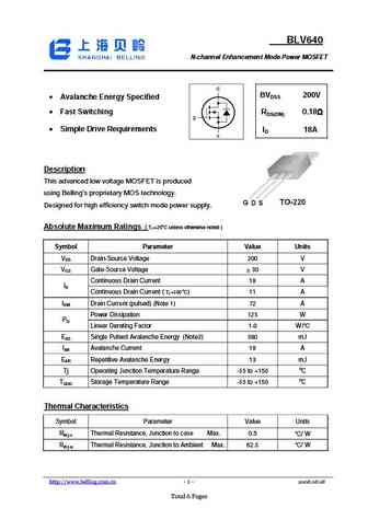
BLV640 N-channel Enhancement Mode Power MOSFET 200V DSS Avalanche Energy Specified BV Fast Switching RDS(ON) 0.18 Simple Drive Requirements ID 18A Description This advanced low voltage MOSFET is produced using Belling s proprietary MOS technology. Designed for high efficiency switch mode power supply. Absolute Maximum Ratings ( TC=25oC unless
chm640ngp.pdf
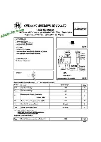
CHENMKO ENTERPRISE CO.,LTD CHM640NGP SURFACE MOUNT N-Channel Enhancement Mode Field Effect Transistor VOLTAGE 200 Volts CURRENT 18 Ampere APPLICATION * Servo motor control. * Power MOSFET gate drivers. * Other switching applications. D2PAK FEATURE * Small package. (D2PAK) 0.420(10.67) 0.190(4.83) * Super high dense cell design for extremely low RDS(ON). 0.380(9.69) 0.160(4.0
csd16409q3.pdf
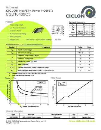
N-Channel CICLON NexFET Power MOSFETs CSD16409Q3 Features Product Summary Ultra Low Qg & Qgd VDS 25 V S 1 8 D S 1 8 D Qg 4.0 nC Low Thermal Resistance G D S 2 7 D S 2 7 D Qgd 1.0 nC S D Avalanche Rated D S S 3 6 D VGS=4.5V 9.5 m S 3 6 D D RDS(on) S D D G 4 5 D G 4 5 D VGS=10V 6.2 m Pb Free Terminal Plating Vth 2.0 V RoHS Comp
csd16404q5a.pdf
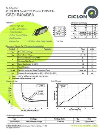
N-Channel CICLON NexFET Power MOSFETs CSD16404Q5A Features Product Summary Ultra Low Qg & Qgd VDS 25 V D S 1 8 D S 1 8 D Qg 6.5 nC Low Thermal Resistance D S 2 7 D G S 2 7 D Qgd 1.7 nC D Avalanche Rated S D S 3 6 D S 3 6 D VGS=4.5V 5.7 m S RDS(on) D D G 4 5 D G 4 5 D VGS=10V 4.1 m Pb Free Terminal Plating S Vth 1.8 V RoHS Compl
csd16407q5.pdf
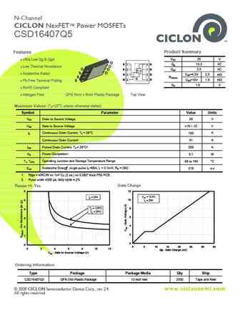
N-Channel CICLON NexFET Power MOSFETs CSD16407Q5 Product Summary Features Ultra Low Qg & Qgd VDS 25 V D S 1 8 D S 1 8 D Qg 13.3 nC Low Thermal Resistance D S 2 7 D G S 2 7 D Qgd 3.5 nC D Avalanche Rated S D S 3 6 D S 3 6 D VGS=4.5V 2.5 m S RDS(on) D D G 4 5 D G 4 5 D VGS=10V 1.8 m Pb Free Terminal Plating S Vth 1.6 V RoHS Compli
csd16403q5a.pdf
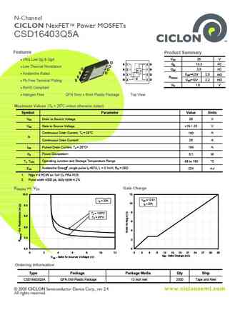
N-Channel CICLON NexFET Power MOSFETs CSD16403Q5A Features Product Summary Ultra Low Qg & Qgd VDS 25 V D S 1 8 D S 1 8 D Qg 13.3 nC Low Thermal Resistance D S 2 7 D G S 2 7 D Qgd 3.5 nC D Avalanche Rated S D S 3 6 D S 3 6 D VGS=4.5V 2.9 m S RDS(on) D D G 4 5 D G 4 5 D VGS=10V 2.2 m Pb Free Terminal Plating S Vth 1.6 V RoHS Complia
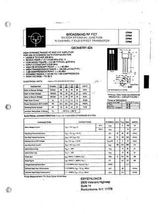
elm36403ea.pdf
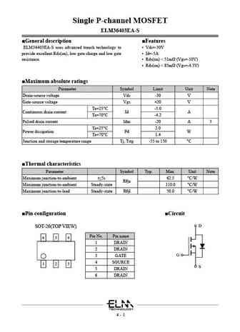
Single P-channel MOSFET ELM36403EA-S General description Features ELM36403EA-S uses advanced trench technology to Vds=-30V provide excellent Rds(on), low gate charge and low gate Id=-5A resistance. Rds(on)
elm16405ea.pdf

Single P-channel MOSFET ELM16405EA-S General description Features ELM16405EA-S uses advanced trench technology to Vds=-30V provide excellent Rds(on), low gate charge and low gate Id=-5A (Vgs=-10V) resistance. Rds(on)
elm36402ea.pdf
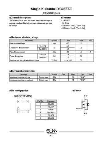
Single N-channel MOSFET ELM36402EA-S General description Features ELM36402EA-S uses advanced trench technology to Vds=20V provide excellent Rds(on), low gate charge and low gate Id=6.5A resistance. Rds(on)
elm16408ea.pdf
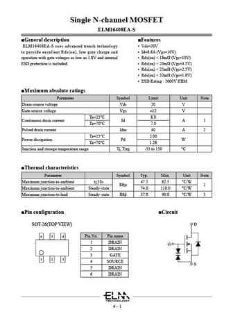
Single N-channel MOSFET ELM16408EA-S General description Features ELM16408EA-S uses advanced trench technology Vds=20V to provide excellent Rds(on), low gate charge and Id=8.8A (Vgs=10V) operation with gate voltages as low as 1.8V and internal Rds(on)
elm36400ea.pdf
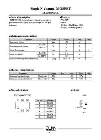
Single N-channel MOSFET ELM36400EA-S General description Features ELM36400EA-S uses advanced trench technology to Vds=30V provide excellent Rds(on), low gate charge and low gate Id=7A resistance. Rds(on)
elm16401ea.pdf
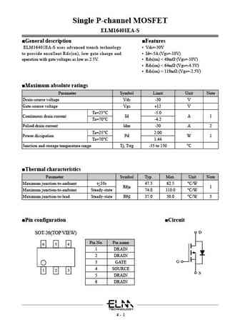
Single P-channel MOSFET ELM16401EA-S General description Features ELM16401EA-S uses advanced trench technology Vds=-30V to provide excellent Rds(on), low gate charge and Id=-5A (Vgs=-10V) operation with gate voltages as low as 2.5V. Rds(on)
elm16402ea.pdf

Single N-channel MOSFET ELM16402EA-S General description Features ELM16402EA-S uses advanced trench technology to Vds=30V provide excellent Rds(on), low gate charge and low gate Id=6.9A (Vgs=10V) resistance. Rds(on)
elm16409ea.pdf
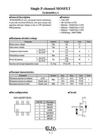
Single P-channel MOSFET ELM16409EA-S General description Features ELM16409EA-S uses advanced trench technology Vds=-20V to provide excellent Rds(on), low gate charge and Id=-5A (Vgs=-4.5V) operation with gate voltages as low as 1.8V and internal Rds(on)
elm36405ea.pdf
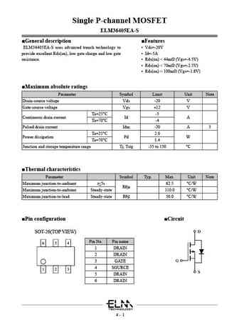
Single P-channel MOSFET ELM36405EA-S General description Features ELM36405EA-S uses advanced trench technology to Vds=-20V provide excellent Rds(on), low gate charge and low gate Id=-5A resistance. Rds(on)
elm16403ea.pdf

Single P-channel MOSFET ELM16403EA-S General description Features ELM16403EA-S uses advanced trench technology to Vds=-30V provide excellent Rds(on), low gate charge and low gate Id=-6A (Vgs=-10V) resistance. Rds(on)
elm16400ea.pdf
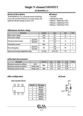
Single N-channel MOSFET ELM16400EA-S General description Features ELM16400EA-S uses advanced trench technology Vds=30V to provide excellent Rds(on), low gate charge and Id=6.9A (Vgs=10V) operation with gate voltages as low as 2.5V. Rds(on)
fhp640a.pdf
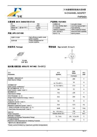
N N-CHANNEL MOSFET FHP640A MAIN CHARACTERISTICS FEATURES ID 18A Low gate charge VDSS 200V Crss ( 26pF) Low Crss (typical 26pF ) Rdson-typ @Vgs=10V 0.125 Fast switching Qg-typ 20nC 100% 100% avalanche tested dv/dt Improved dv/dt
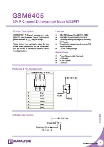
mg06400d-bn4mm.pdf
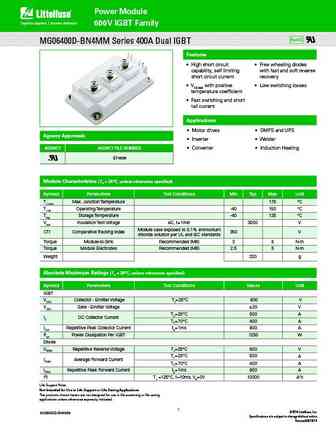
Power Module 600V IGBT Family RoHS MG06400D-BN4MM Series 400A Dual IGBT Features High short circuit Free wheeling diodes capability, self limiting with fast and soft reverse short circuit current recovery VCE(sat) with positive Low switching losses temperature coefficient Fast switching and short tail current Applications Motor drives SMPS and UP
mg06400d-bn1mm.pdf
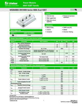
Power Module 600V IGBT Family RoHS MG06400D-BN1MM Series 400A Dual IGBT Features Ultra low loss Positive temperature coefficient High ruggedness High short circuit capability Applications Motor drives SMPS and UPS Inverter Welder Agency Approvals Converter Induction Heating AGENCY AGENCY FILE NUMBER E71639 Module Characteristics (T
me7640 me7640-g.pdf
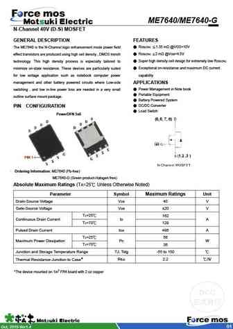
ME7640/ME7640-G N-Channel 40V (D-S) MOSFET GENERAL DESCRIPTION FEATURES The ME7640 is the N-Channel logic enhancement mode power field RDS(ON) 1.35 m @VGS=10V effect transistors are produced using high cell density , DMOS trench RDS(ON) 2 m @VGS=4.5V technology. This high density process is especially tailored to Super high density cell design for extremely low RD
nce60n640f.pdf
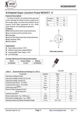
NCE60N640F N-Channel Super Junction Power MOSFET General Description The series of devices use advanced trench gate super V 650 V DS min@Tjmax junction technology and design to provide excellent RDS(ON) R 580 m DS(ON)TYP. with low gate charge. This super junction MOSFET fits the I 6.7 A D industry s AC-DC SMPS requirements for PFC, AC/DC Qg 11 nC power conversion, and indus
nce60n640k.pdf
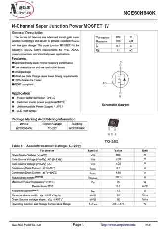
NCE60N640K N-Channel Super Junction Power MOSFET General Description The series of devices use advanced trench gate super V 650 V DS min@Tjmax junction technology and design to provide excellent RDS(ON) R 580 m DS(ON)TYP. with low gate charge. This super junction MOSFET fits the I 6.7 A D industry s AC-DC SMPS requirements for PFC, AC/DC Qg 11 nC power conversion, and indus
nce60n640i.pdf
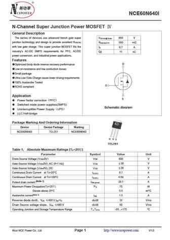
NCE60N640I N-Channel Super Junction Power MOSFET General Description The series of devices use advanced trench gate super V 650 V DS min@Tjmax junction technology and design to provide excellent RDS(ON) R 580 m DS(ON)TYP. with low gate charge. This super junction MOSFET fits the I 6.7 A D industry s AC-DC SMPS requirements for PFC, AC/DC Qg 11 nC power conversion, and indus
nce60n640d.pdf
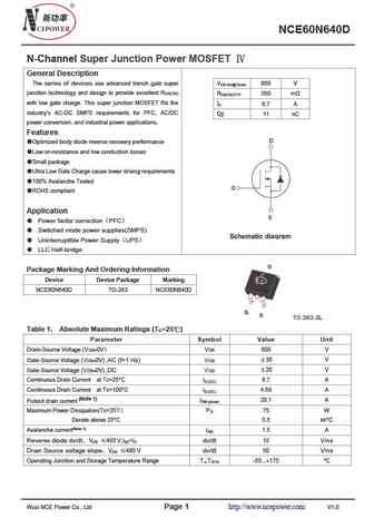
NCE60N640D N-Channel Super Junction Power MOSFET General Description The series of devices use advanced trench gate super V 650 V DS min@Tjmax junction technology and design to provide excellent RDS(ON) R 580 m DS(ON)TYP. with low gate charge. This super junction MOSFET fits the I 6.7 A D industry s AC-DC SMPS requirements for PFC, AC/DC Qg 11 nC power conversion, and indus
nce60n640.pdf
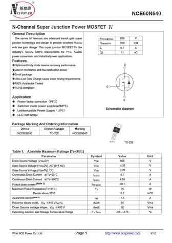
NCE60N640 N-Channel Super Junction Power MOSFET General Description The series of devices use advanced trench gate super V 650 V DS min@Tjmax junction technology and design to provide excellent RDS(ON) R 580 m DS(ON)TYP. with low gate charge. This super junction MOSFET fits the I 6.7 A D industry s AC-DC SMPS requirements for PFC, AC/DC Qg 11 nC power conversion, and indust
swp640d swy640d swb640d.pdf
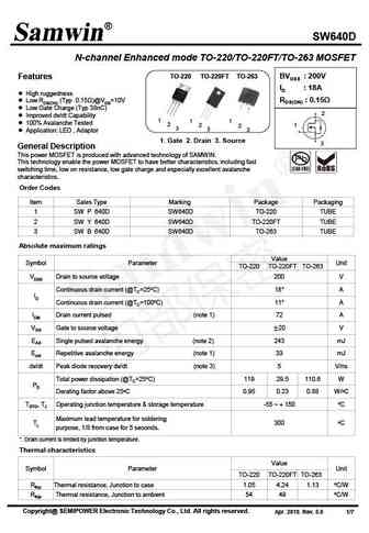
SW640D N-channel Enhanced mode TO-220/TO-220FT/TO-263 MOSFET TO-220 TO-220FT TO-263 BVDSS 200V Features ID 18A High ruggedness RDS(ON) 0.15 Low RDS(ON) (Typ 0.15 )@VGS=10V Low Gate Charge (Typ 38nC) 2 Improved dv/dt Capability 1 1 1 100% Avalanche Tested 2 1 2 2 3 3 3 Application LED , Adaptor 1. Gate 2. Drain 3. Sour
hfs640.pdf
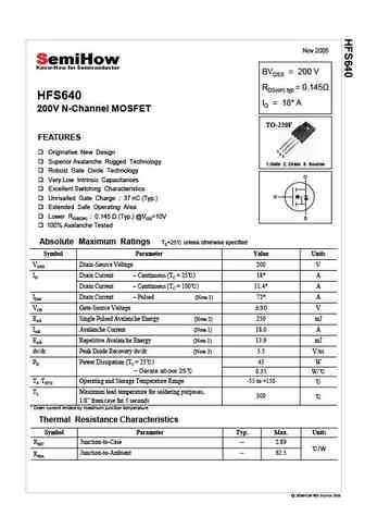
Nov 2005 BVDSS = 200 V RDS(on) typ HFS640 ID = 18* A 200V N-Channel MOSFET TO-220F FEATURES 1 Originative New Design 2 3 Superior Avalanche Rugged Technology 1.Gate 2. Drain 3. Source Robust Gate Oxide Technology D Very Low Intrinsic Capacitances Excellent Switching Characteristics G Unrivalled Gate Charge 37 nC (Typ.) Extended Safe Operating Area
hfi640 hfw640.pdf
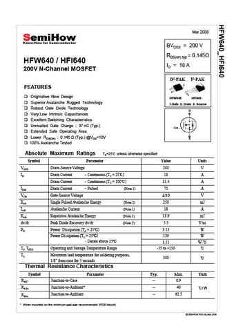
Mar 2008 BVDSS = 200 V RDS(on) typ HFW640 / HFI640 ID = 18 A 200V N-Channel MOSFET D2-PAK I2-PAK 2 FEATURES 1 3 1 2 3 Originative New Design HFW640 HFI640 Superior Avalanche Rugged Technology 1.Gate 2. Drain 3. Source Robust Gate Oxide Technology Very Low Intrinsic Capacitances Excellent Switching Characteristics Unrivalled Gate Charge 37 nC (Typ.)
shd226403 shd226403r.pdf
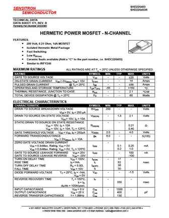
SHD226403 SENSITRON SHD226403R SEMICONDUCTOR TECHNICAL DATA DATA SHEET 171, REV. B Formerly Part Number SHD2263 HERMETIC POWER MOSFET - N-CHANNEL FEATURES 200 Volt, 0.21 Ohm, 14A MOSFET Isolated Hermetic Metal Package Fast Switching Low RDS (on) Ceramic Seals available (Add a C to the part number, i.e. SHDC226403) Similar to IRFY240
shd226409.pdf
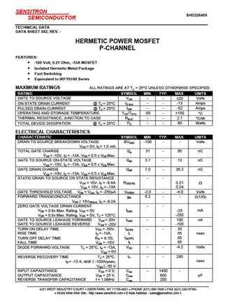
SENSITRON SHD226409 SEMICONDUCTOR TECHNICAL DATA DATA SHEET 582, REV. - HERMETIC POWER MOSFET P-CHANNEL FEATURES -100 Volt, 0.21 Ohm, -13A MOSFET Isolated Hermetic Metal Package Fast Switching Equivalent to IRFY9140 Series MAXIMUM RATINGS ALL RATINGS ARE AT TC = 25 C UNLESS OTHERWISE SPECIFIED. RATING SYMBOL MIN. TYP. MAX. UNITS GATE TO SOURCE VOLT
shd226405.pdf
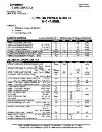
SHD226405 SENSITRON SHD226405B SEMICONDUCTOR TECHNICAL DATA DATA SHEET 2037, REV. C HERMETIC POWER MOSFET N-CHANNEL FEATURES 500 Volt, 0.85, Ohm, 7A MOSFET Isolated Hermetically Sealed MAXIMUM RATINGS ALL RATINGS ARE AT TA = 25 C UNLESS OTHERWISE SPECIFIED. RATING SYMBOL MIN. TYP. MAX. UNITS GATE TO SOURCE VOLTAGE VGS - - 20 Volts ID - - 7 Amps
shd226408.pdf
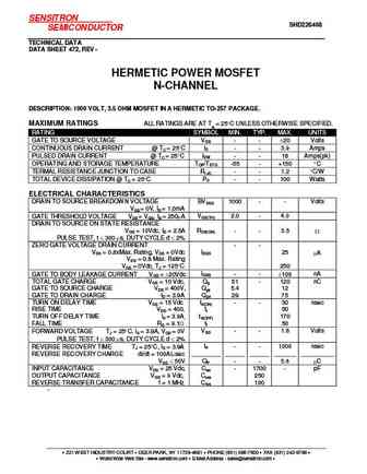
SENSITRON SHD226408 SEMICONDUCTOR TECHNICAL DATA DATA SHEET 472, REV - HERMETIC POWER MOSFET N-CHANNEL DESCRIPTION 1000 VOLT, 3.5 OHM MOSFET IN A HERMETIC TO-257 PACKAGE. MAXIMUM RATINGS ALL RATINGS ARE AT TA = 25 C UNLESS OTHERWISE SPECIFIED. RATING SYMBOL MIN. TYP. MAX. UNITS GATE TO SOURCE VOLTAGE VGS - - 20 Volts ID - - 3.9 Amps CONTINUOUS DRAIN CURRENT @ TC = 25 C ID
shd226401.pdf
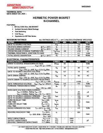
SENSITRON SHD226401 SEMICONDUCTOR TECHNICAL DATA DATA SHEET 581, REV. - HERMETIC POWER MOSFET N-CHANNEL FEATURES 60 Volt, 0.035 Ohm, 20A MOSFET Isolated Hermetic Metal Package Fast Switching Low R DS (on) Equivalent to IRFY044 Series MAXIMUM RATINGS ALL RATINGS ARE AT TC = 25 C UNLESS OTHERWISE SPECIFIED. RATING SYMBOL MIN. TYP. MAX. UNITS GATE TO SOURCE VOLTA
shd226404.pdf
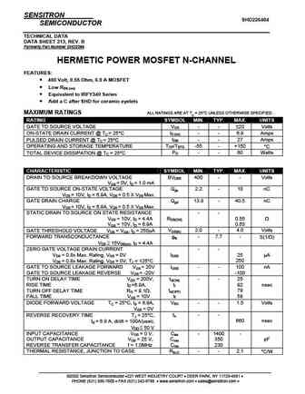
SENSITRON SHD226404 SEMICONDUCTOR TECHNICAL DATA DATA SHEET 213, REV. B Formerly Part Number SHD2264 HERMETIC POWER MOSFET N-CHANNEL FEATURES 400 Volt, 0.55 Ohm, 6.9 A MOSFET Low RDS (on) Equivalent to IRFY340 Series Add a C after SHD for ceramic eyelets MAXIMUM RATINGS ALL RATINGS ARE AT TC = 25 C UNLESS OTHERWISE SPECIFIED. RATING SYMBOL MIN. TYP.
shd226402.pdf
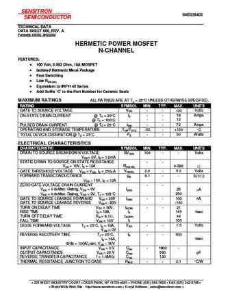
SENSITRON SHD226402 SEMICONDUCTOR TECHNICAL DATA DATA SHEET 606, REV. A Formerly DS302, SHD2262 HERMETIC POWER MOSFET N-CHANNEL FEATURES 100 Volt, 0.092 Ohm, 18A MOSFET Isolated Hermetic Metal Package Fast Switching Low RDS (on) Equivalent to IRFY140 Series Add Suffix C to the Part Number for Ceramic Seals MAXIMUM RATINGS ALL RATINGS ARE AT TC = 25 C
3cg640.pdf
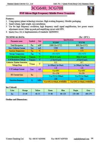
Shaanxi Qunli Electric Co., Ltd Add. No. 1 Qunli Road,Baoji City,Shaanxi,China 3CG640, 3CG708 PNP Silicon High Frequency Middle Power Transistor Features 1. Using epitaxy planar technology structure. High working frequency. Metallic packaging. 2. Small volume, light weight, easy installation. 3. Use for high frequency oscillation, high frequency small signal amplification, low powe
irlml6401.pdf
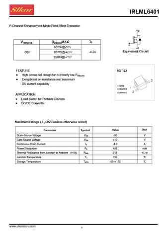
IRLML6401 P-Channel Enhancement Mode Field Effect Transistor D ID V(BR)DSS RDS(on)MAX G m @-10V 60 S Equivalent Circuit -30V 70 m -4.2A @-4.5V m @-2.5V 85 FEATURE SOT-23 High dense cell design for extremely low RDS(ON) Exceptional on-resistance and maximum DC current capability 1. GATE 2. SOURCE 3. DRAIN D APPLICATION Load Switch for Portable Devic
irlml6402.pdf
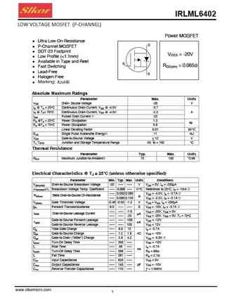
IRLML6402 LOW VOLTAGE MOSFET (P-CHANNEL) Power MOSFET l Ultra Low On-Resistance D l P-Channel MOSFET l SOT-23 Footprint VDSS = -20V l Low Profile (
irf640.pdf
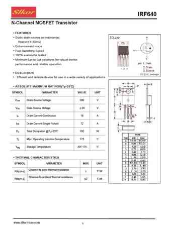
IRF640 N-Channel MOSFET Transistor FEATURES Static drain-source on-resistance TO-220 RDS(on) 150m Enhancement mode Fast Switching Speed 100% avalanche tested Minimum Lot-to-Lot variations for robust device performance and reliable operation DESCRITION Efficient and reliable device for use in a wide variety of applications ABSOLUTE MAXIMUM RATINGS(T =25 )
sl1640.pdf
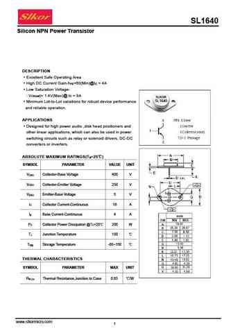
SL1640 Silicon NPN Power Transistor DESCRIPTION Excellent Safe Operating Area High DC Current Gain-h =60(Min)@I = 4A FE C Low Saturation Voltage- V )= 1.4V(Max)@ I = 8A CE(sat C SLKOR SL1640 Minimum Lot-to-Lot variations for robust device performance and reliable operation. APPLICATIONS Designed for high power audio ,disk head positioners and other linear applications
irlml6401.pdf
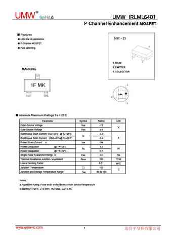
R UMWp UMW IRLML6401 UMW IRLML6401 UMW IRLML6401 Ty P-Channel Enhancement MOSFET Features SOT 23 Ultra low on-resistance. P-Channel MOSFET. Fast switching. 1. BASE 2. EMITTER MARKING 3. COLLECTOR 1F MK Absolute Maximum Ratings Ta = 25 Parameter Symbol Rating Unit Drain-Source Voltage VDS -12 V Gate-Source Voltage VGS 8 Continuous Drain Cu
irlml6402.pdf
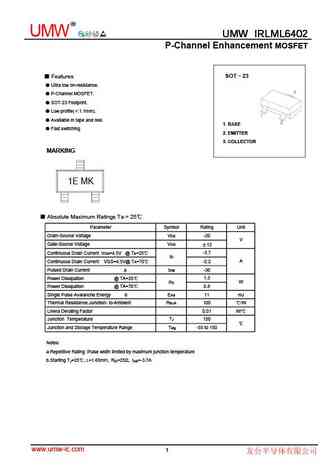
R UMW UMW IRLML6402 UMW IRLML6402 UMW IRLML6402 P-Channel Enhancement MOSFET SOT 23 Features Ultra low on-resistance. P-Channel MOSFET. SOT-23 Footprint. Low profile( 1.1mm). Available in tape and reel. 1. BASE Fast switching. 2. EMITTER 3. COLLECTOR MARKING 1E MK Absolute Maximum Ratings Ta = 25 Parameter Symbol Rating Unit Drai
cs640fa9h.pdf
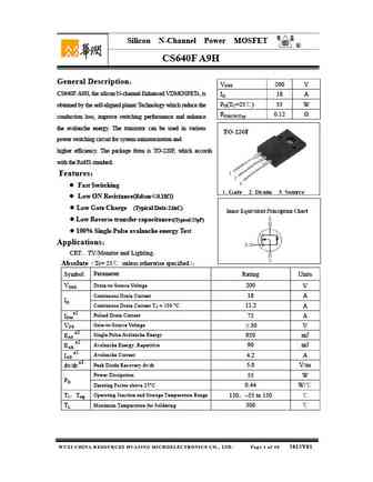
Silicon N-Channel Power MOSFET R CS640F A9H General Description VDSS 200 V CS640F A9H, the silicon N-channel Enhanced VDMOSFETs, is ID 18 A PD(TC=25 ) 55 W obtained by the self-aligned planar Technology which reduce the RDS(ON)Typ 0.12 conduction loss, improve switching performance and enhance the avalanche energy. The transistor can be used in various pow
cs640a8h.pdf
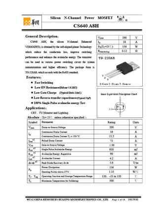
Silicon N-Channel Power MOSFET R CS640 A8H General Description VDSS 200 V CS640 A8H, the silicon N-channel Enhanced ID 18 A PD(TC=25 ) 156 W VDMOSFETs, is obtained by the self-aligned planar Technology RDS(ON)Typ 0.12 which reduce the conduction loss, improve switching performance and enhance the avalanche energy. The transistor can be used in various power s
cs640a0h.pdf
Silicon N-Channel Power MOSFET R CS640 A0H General Description VDSS 200 V CS640 A0H, the silicon N-channel Enhanced VDMOSFETs, is ID 18 A PD(TC=25 ) 156 W obtained by the self-aligned planar Technology which reduce the RDS(ON)Typ 0.12 conduction loss, improve switching performance and enhance the avalanche energy. The transistor can be used in various power
atm6402nsa.pdf

ATM6402NSA N-Channel Enhancement Mode Field Effect Transistor Description Feature The ATM6402NSA uses advanced trench technology V (V) = 30V DS to provide excellent R , low gate charge and DS(ON) I = 6.1A (V = 10V) D GS operation with gate voltages as low as 4.5V. This R
irlml6401.pdf
IRLML6401 P-Channel MOSFET Features Pin Configurations V = -12V DS I D = -4.3A R @V = -4.5V, MAX =50m DS(ON) GS R @V = -2.5V, MAX =85m DS(ON) GS General Description Fast switching High Density Cell Design For Ultra Low On-Resistance SOT-23-3L for Surface Mount Package. Absolute Maximum Ratings @T =25 unless otherwise noted A Parameter Symbol
bml6401.pdf
BML6401 MOSFET ROHS P-Channel MOSFET SOT-23 - Features Ultra low on-resistance. Fast switching. Marking 6401 Maximum Ratings & Thermal Characteristics (Ratings at 25 ambient temperature unless otherwise specified.) Parameter Symbol Rating Unit Drain-Source Voltage VDS -12 V Gate-Source Voltage VGS 8 ID Continuous Drain Current VGS=4.5V @ TA=25 -4.3
irlml6402.pdf
IRLML6402 P-Channel MOSFET Features Pin Configurations V = -20V DS I D = -3.7A R @V = -4.5V, TYP =50m DS(ON) GS R @V = -2.5V, TYP =80m DS(ON) GS General Description Advanced tr ench process technology High Density Cell Design For Ultra Low On-Resistance SOT-23 for Surface Mount Package. Absolute Maximum Ratings @T =25 unless otherwise noted A
bml6402.pdf
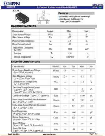
BML6402 MOSFET ROHS P-Channel Enhancement-Mode MOSFET SOT-23 - Features Advanced trench process technology High Density Cell Design For Ultra Low On-Resistance MAXIMUM RANTINGS Characteristic Symbol Max Unit Drain-Source Voltage BV -20 V DSS Gate- Source Voltage V +12 V GS Drain Current (continuous) I -3.7 A D Drain Current (pulsed) I -15 A DM Total Device Dis
hf640 hp640.pdf
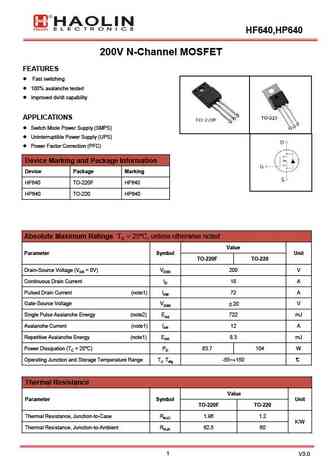
HF640,HP640 200V N-Channel MOSFET FEATURES Fast switching 100% avalanche tested Improved dv/dt capability APPLICATIONS Switch Mode Power Supply (SMPS) Uninterruptible Power Supply (UPS) Power Factor Correction (PFC) Device Marking and Package Information Device Package Marking HF640 TO-220F HF640 HP640 TO-220 HP640 Absolute Maximum Ratings TC = 25 C, unles
irlml6401.pdf
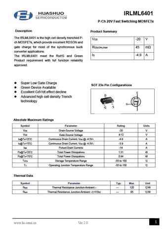
IRLML6401 P-Ch 20V Fast Switching MOSFETs Description Product Summary The IRLML6401 is the high cell density trenched P- VDS -20 V ch MOSFETs, which provide excellent RDSON and gate charge for most of the synchronous buck RDS(ON),max 45 m converter applications. ID -4.9 A The IRLML6401 meet the RoHS and Green Product requirement with full function reliability approved
irlml6402.pdf

IRLML6402 P-Ch 20V Fast Switching MOSFETs Description Product Summary The IRLML6402 is the high cell density trenched P- VDS -20 V ch MOSFETs, which provide excellent RDSON and gate charge for most of the synchronous buck RDS(ON),max 45 m converter applications. ID -4.9 A The IRLML6402 meet the RoHS and Green Product requirement with full function reliability approved
jmh65r640ak.pdf
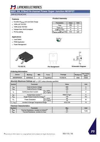
650V, 9A, 578m N-channel Power Super Junction MOSFET JMH65R640AK Product Summary Features Excellent RDS(ON) and Low Gate Charge Parameters Value Unit 100% UIS TESTED VDSS 650 V 100% Vds TESTED VGS(th)_Typ 3.1 V Halogen-free; RoHS-compliant ID(@VGS=10V) 9 A Pb-free plating RDS(ON)_Typ(@VGS=10V 578 mW Applications Load Switch PWM Application Pow
lsc70r640gt lsd70r640gt lsg70r640gt lsh70r640gt lsf70r640gt.pdf
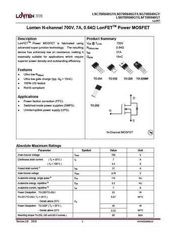
LSC70R640GT/LSD70R640GT/LSG70R640GT/ LSH70R640GT/LSF70R640GT LonFET Lonten N-channel 700V, 7A, 0.64 LonFETTM Power MOSFET Description Product Summary LonFETTM Power MOSFET is fabricated using VDS @ Tj,max 750V advanced super junction technology. The resulting RDS(on),max 0.64 device has extremely low on resistance, making it IDM 21A especially suitable for applications whic
irf640n.pdf
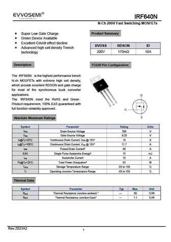
IRF640N N-Ch 200V Fast Switching MOSFETs Product Summary Super Low Gate Charge Green Device Available Excellent Cdv/dt effect decline BVDSS RDSON ID Advanced high cell density Trench 200V 170m 18A technology Description TO220 Pin Configuration The IRF640N is the highest performance trench N-ch MOSFETs with extreme high cell density, which provide excel
irlml6401.pdf
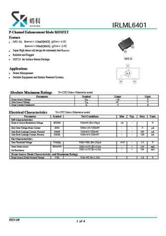
IRLML6401 P-Channel Enhancement Mode MOSFET Feature DS(ON) GS -16V/-3A, R = 110m (MAX) @V = -4.5V. DS(ON) GS R = 140m (MAX) @V = -2.5V. DS(ON) Super High dense cell design for extremely low R Reliable and Rugged SOT-23 SOT-23 for Surface Mount Package Applications Power Management Portable Equipment and Battery Powered Systems. A T =25 Unless
irlml6402.pdf
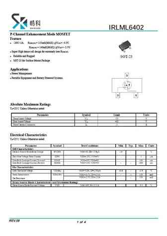
IRLML6402 P-Channel Enhancement Mode MOSFET Channel Enhancement Mode MOSFET Feature -20V/-3A, RDS(ON) = 125m (MAX) @VGS = -4.5V. GS RDS(ON) = 140m (MAX) @VGS = -2.5V. GS Super High dense cell design for extremely low R Super High dense cell design for extremely low RDS(ON) Reliable and Rugged SOT-23 for Surface Mount Package Applications Power Managem
hgn640n25s.pdf
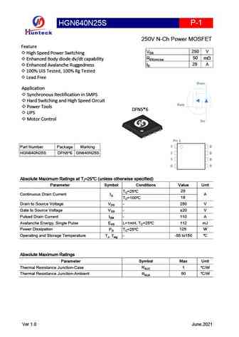
HGN640N25S P-1 250V N-Ch Power MOSFET Feature 250 V VDS High Speed Power Switching 50 RDS(on),typ mW Enhanced Body diode dv/dt capability 29 A ID Enhanced Avalanche Ruggedness 100% UIS Tested, 100% Rg Tested Lead Free Drain Application Synchronous Rectification in SMPS Hard Switching and High Speed Circuit Gate Power Tools DFN5*6
hgb640n25s hgk640n25s hgp640n25s.pdf
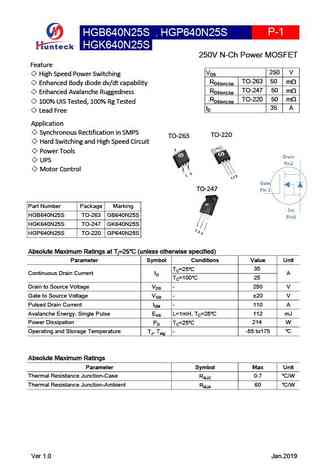
, HGB640N25S HGP640N25S P-1 HGK640N25S 250V N-Ch Power MOSFET Feature 250 V VDS High Speed Power Switching TO-263 50 RDS(on),typ m Enhanced Body diode dv/dt capability TO-247 50 RDS(on),typ m Enhanced Avalanche Ruggedness TO-220 50 RDS(on),typ m 100% UIS Tested, 100% Rg Tested 35 A ID Lead Free Application Synchronous Rectification in SMPS
irlml6401.pdf
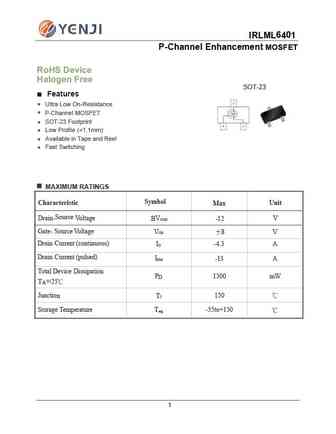
IRLML6401 P-Channel Enhancement MOSFET RoHS Device Halogen Free SOT-23 Features l Ultra Low On-Resistance l P-Channel MOSFET l SOT-23 Footprint l Low Profile (
wst6401.pdf
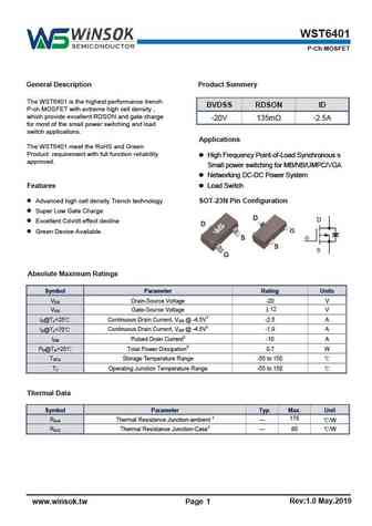
WST6401 P-Ch MOSFET General Description Product Summery The WST6401 is the highest performance trench BVDSS RDSON ID P-ch MOSFET with extreme high cell density , which provide excellent RDSON and gate charge -20V 135m -2.5A for most of the small power switching and load switch applications. Applications The WST6401 meet the RoHS and Green Product requirement with full fu
wst6402.pdf
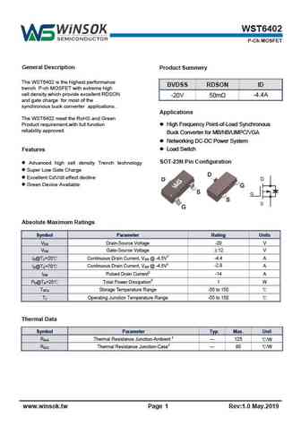
WST6402 P-Ch MOSFET General Description Product Summery The WST6402 is the highest performance BVDSS RDSON ID trench P-ch MOSFET with extreme high cell density,which provide excellent RDSON -4.4A -20V 50m and gate charge for most of the synchronous buck converter applications . Applications The WST6402 meet the RoHS and Green Product requirement,with full function Hig
vs6640ac.pdf
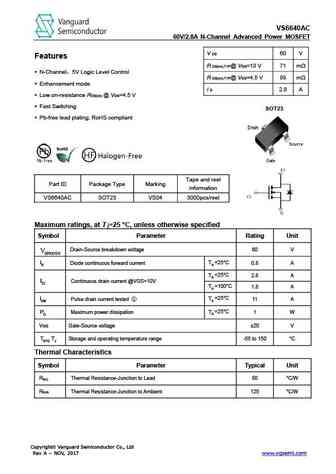
VS6640AC 60V/2.8A N-Channel Advanced Power MOSFET V DS 60 V Features R DS(on),TYP@ VGS=10 V 71 m N-Channel 5V Logic Level Control R DS(on),TYP@ VGS=4.5 V 89 m Enhancement mode I D 2.8 A Low on-resistance RDS(on) @ VGS=4.5 V Fast Switching SOT23 Pb-free lead plating; RoHS compliant Tape and reel Part ID Package Type Marking information
vs3640ds.pdf
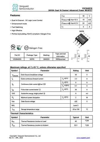
VS3640DS 30V/9A Dual N-Channel Advanced Power MOSFET Features V DS 30 V R DS(on),TYP@ VGS=10 V 16 m Dual N-Channel 5V Logic Level Control R DS(on),TYP@ VGS=4.5 V 24 m Enhancement mode I D 9 A Fast Switching High Effective SOP8 Pb-free lead plating; RoHS compliant; Halogen-Free Tape and reel Part ID Package Type Marking information VS
sm66406d1rl.pdf
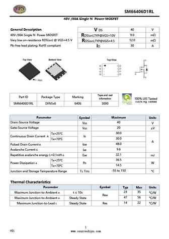
SM66406D1RL 40V /30A Single N Power MOSFET D N04D N 40V /30A Single N Power MOSFET 30N04D General Description 40 V V DS 40V /30A Single N Power MOSFET 9.0 m RDS(on),TYP@VGS=10V Very low on-resistance RDS(on) @ VGS=4.5 V 12.0 m RDS(on),TYP@VGS=4.5 Pb-free lead plating; RoHS compliant 30 A ID Tape and reel Part ID Package Type Marking infomation 100% UIS Tested 100% Rg Tested
ao6403.pdf
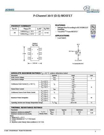
AO6403 www.VBsemi.tw P-Channel 30-V (D-S) MOSFET FEATURES PRODUCT SUMMARY Halogen-free According to IEC 61249-2-21 VDS (V) RDS(on) ( ) ID (A)a Qg (Typ.) Available 0.049 at VGS = - 10 V - 4.8 TrenchFET Power MOSFET - 30 5.1 nC 0.054 at VGS = - 4.5 V - 4.1 APPLICATIONS Load Switch TSOP-6 (4) S Top V iew 1 6 (3) G 3 mm 5 2 3 4 (1, 2, 5, 6) D 2.85 mm P-Chan
ipd640n06lg.pdf
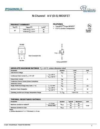
IPD640N06LG www.VBsemi.tw N-Channel 6 0-V (D-S) MOSFET FEATURES PRODUCT SUMMARY TrenchFET Power MOSFET VDS (V) rDS(on) ( ) ID (A)a Available 175 C Junction Temperature 0.025 at VGS = 10 V 35 RoHS* 60 0.030 at VGS = 4.5 V 30 COMPLIANT TO-252 D G Drain Connected to Tab G D S S Top View N-Channel MOSFET ABSOLUTE MAXIMUM RATINGS TC = 25 C, unless otherwise n
irlml6401gtrpbf.pdf
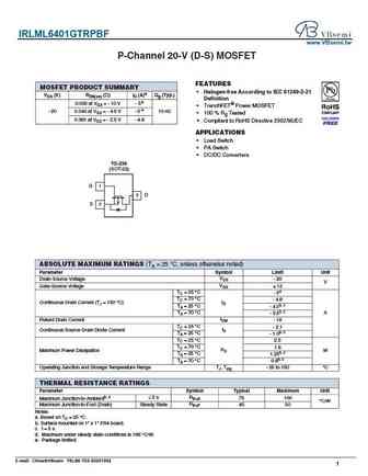
IRLML6401GTRPBF www.VBsemi.tw P-Channel 20-V (D-S) MOSFET FEATURES MOSFET PRODUCT SUMMARY Halogen-free According to IEC 61249-2-21 VDS (V) RDS(on) ( )ID (A)a Qg (Typ.) Definition 0.035 at VGS = - 10 V - 5e TrenchFET Power MOSFET e - 20 0.043 at VGS = - 4.5 V - 5 10 nC 100 % Rg Tested 0.061 at VGS = - 2.5 V - 4.8 Compliant to RoHS Directive 2002/95/EC APPLICAT
irlml6401trpbf.pdf

IRLML6401TRPBF www.VBsemi.tw P-Channel 20-V (D-S) MOSFET FEATURES MOSFET PRODUCT SUMMARY Halogen-free According to IEC 61249-2-21 VDS (V) RDS(on) ( )ID (A)a Qg (Typ.) Definition 0.035 at VGS = - 10 V - 5e TrenchFET Power MOSFET e - 20 0.043 at VGS = - 4.5 V - 5 10 nC 100 % Rg Tested 0.061 at VGS = - 2.5 V - 4.8 Compliant to RoHS Directive 2002/95/EC APPLICATI
ao6400.pdf
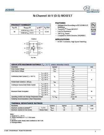
AO6400 www.VBsemi.tw N-Channel 30 V (D-S) MOSFET FEATURES PRODUCT SUMMARY Halogen-free According to IEC 61249-2-21 Definition VDS (V) RDS(on) ( ) ID (A)a, e Qg (Typ.) TrenchFET Power MOSFET 0.030 at VGS = 10 V 6 Low On-Resistance 30 4.2 nC 0.040 at VGS = 4.5 V 6 100 % Rg Tested Compliant to RoHS Directive 2002/95/EC TSOP-6 APPLICATIONS DC/DC Co
ao6409.pdf
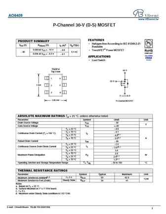
AO6409 www.VBsemi.tw P-Channel 30-V (D-S) MOSFET FEATURES PRODUCT SUMMARY Halogen-free According to IEC 61249-2-21 VDS (V) RDS(on) ( ) ID (A)a Qg (Typ.) Available 0.049 at VGS = - 10 V - 4.8 TrenchFET Power MOSFET - 30 5.1 nC 0.054 at VGS = - 4.5 V - 4.1 APPLICATIONS Load Switch TSOP-6 (4) S Top V iew 1 6 (3) G 3 mm 5 2 3 4 (1, 2, 5, 6) D 2.85 mm P-Chan
csd16406q3.pdf
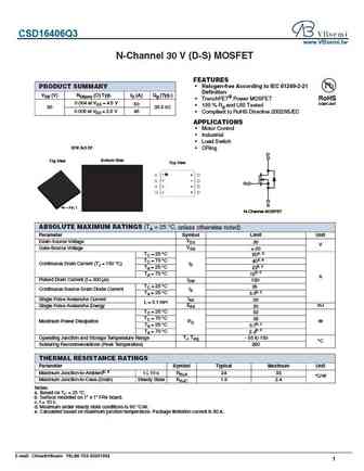
CSD16406Q3 www.VBsemi.tw N-Channel 30 V (D-S) MOSFET FEATURES Halogen-free According to IEC 61249-2-21 PRODUCT SUMMARY Definition VDS (V) RDS(on) ( ) Typ. Qg (Typ.) ID (A) TrenchFET Power MOSFET 0.004 at VGS = 4.5 V 50 100 % Rg and UIS Tested 30 33.5 nC 0.005 at VGS = 2.5 V 45 Compliant to RoHS Directive 2002/95/EC APPLICATIONS Motor Control I
irlml6402trpbf.pdf

IRLML6402TRPBF www.VBsemi.tw P-Channel 20-V (D-S) MOSFET FEATURES MOSFET PRODUCT SUMMARY Halogen-free According to IEC 61249-2-21 VDS (V) RDS(on) ( )ID (A)a Qg (Typ.) Definition 0.035 at VGS = - 10 V - 5e TrenchFET Power MOSFET e - 20 0.043 at VGS = - 4.5 V - 5 10 nC 100 % Rg Tested 0.061 at VGS = - 2.5 V - 4.8 Compliant to RoHS Directive 2002/95/EC APPLICATI
irf640p.pdf
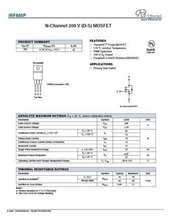
IRF640P www.VBsemi.tw N-Channel 200 V (D-S) MOSFET FEATURES PRODUCT SUMMARY TrenchFET Power MOSFET VDS (V) RDS(on) ( )ID (A) 175 C Junction Temperature 200 0.110 at VGS = 10 V 2 0 PWM Optimized 100 % Rg Tested Compliant to RoHS Directive 2002/95/EC TO-220AB APPLICATIONS Primary Side Switch D DRAIN connected to TAB G G D S Top View S N-Chan
aon6405.pdf
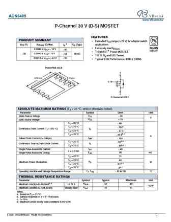
AON6405 www.VBsemi.tw P-Channel 30 V (D-S) MOSFET FEATURES PRODUCT SUMMARY Extended VGS range ( 25 V) for adaptor switch VDS (V) RDS(on) ( ) Max. applications ID a Qg (Typ.) Extremely low RDS(on) 0.0080 at VGS = - 10 V - 60 TrenchFET Power MOSFET - 30 0.0090 at VGS = - 6 V - 53 66 nC 100 % Rg and UIS Tested 0.0012 at VGS = - 4.5 V - 50 Typical ESD Perf
irlml6402g.pdf
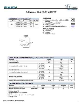
IRLML6402G www.VBsemi.tw P-Channel 20-V (D-S) MOSFET FEATURES MOSFET PRODUCT SUMMARY Halogen-free According to IEC 61249-2-21 VDS (V) RDS(on) ( )ID (A)a Qg (Typ.) Definition 0.035 at VGS = - 10 V - 5e TrenchFET Power MOSFET e - 20 0.043 at VGS = - 4.5 V - 5 10 nC 100 % Rg Tested 0.061 at VGS = - 2.5 V - 4.8 Compliant to RoHS Directive 2002/95/EC APPLICATIONS
tpm6401s3.pdf
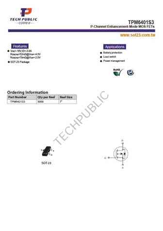
TPM6 4 01 S3 P-Channel Enhancement-Mode MOS FETs www.sot23.com.tw Features Applications VDS=-16V,ID=-3.8A Battery protection RDS(ON)
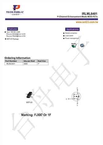
hm6409.pdf
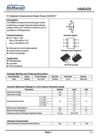
HM6409 P-Channel Enhancement Mode Power MOSFET Description D The HM6409 uses advanced trench technology to provide excellent RDS(ON), low gate charge and operation with gate G voltages as low as 2.5V. This device is suitable for use as a load switch or in PWM applications. S Schematic diagram General Features VDS = -20V,ID = -5.0A RDS(ON)
hm6408.pdf
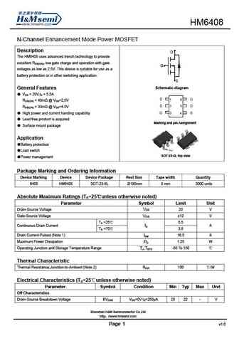
HM6408 N-Channel Enhancement Mode Power MOSFET Description D The HM6408 uses advanced trench technology to provide excellent RDS(ON), low gate charge and operation with gate G voltages as low as 2.5V. This device is suitable for use as a battery protection or in other switching application. S Schematic diagram General Features VDS = 20V,ID = 5.5A RDS(ON)
hm6400.pdf
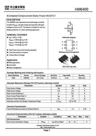
HM6400 N-Channel Enhancement Mode Power MOSFET DESCRIPTION The HM6400 uses advanced trench technology to provide D excellent RDS(ON), low gate charge and operation with gate voltages as low as 2.5V. This device is suitable for use as a G Battery protection or in other Switching application. S GENERAL FEATURES VDS = 30V,ID = 6.9A Schematic diagram RDS(ON)
hm640.pdf
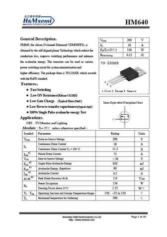
HM640 General Description VDSS 200 V HM640, the silicon N-channel Enhanced VDMOSFETs, is ID 18 A PD(TC=25 ) 156 W obtained by the self-aligned planar Technology which reduce the RDS(ON)Typ 0.12 conduction loss, improve switching performance and enhance the avalanche energy. The transistor can be used in various power switching circuit for system
hm6401.pdf
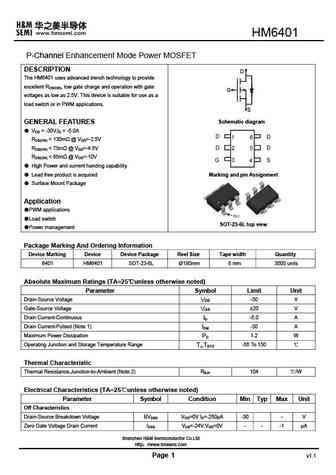
HM6401 P-Channel Enhancement Mode Power MOSFET DESCRIPTION D The HM6401 uses advanced trench technology to provide excellent RDS(ON), low gate charge and operation with gate G voltages as low as 2.5V. This device is suitable for use as a load switch or in PWM applications. S Schematic diagram GENERAL FEATURES VDS = -30V,ID = -5.0A RDS(ON)
irf640ns.pdf
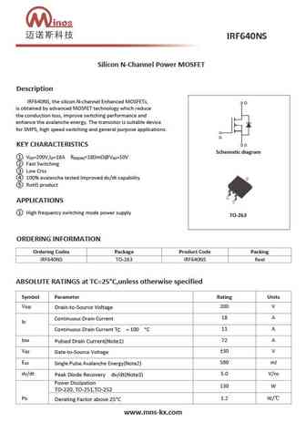
Silicon N-Channel Power MOSFET Description IRF640NS, the silicon N-channel Enhanced MOSFETs, is obtained by advanced MOSFET technology which reduce the conduction loss, improve switching performance and enhance the avalanche energy. The transistor is suitable device for SMPS, high speed switching and general purpose applications. KEY CHARACTERISTICS Schematic diagram V =200V,I =18A
mpsa65m640b.pdf
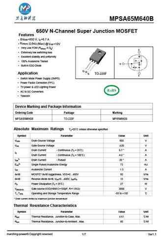
MPSA65M640B 650V N-Channel Super Junction MOSFET Features BV DSS=650 V, I D=6.7 A RDS(on) @ 0.64 (Max) V GS=10V Very Low FOM (RDS(on) X Qg) Extremely low switching loss Excellent stability and uniformity 100% Avalanche Tested Built-in ESD Diode G D Application S TO-220F Switch Mode Power Supply (SMPS) Power Factor Correction (PFC
vs3640aa.pdf
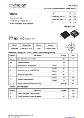
VS3640AA 30V/10A N-Channel Advanced Power MOSFET V DS 30 V Features R DS(on),TYP@ VGS=10 V 14 m Enhancement mode R DS(on),TYP@ VGS=4.5 V 20 m Fast Switching and High efficiency I D 10 A Pb-free lead plating; RoHS compliant DFN2x2x0.75-6L Part ID Package Type Marking Packing VS3640AA DFN2x2x0.75-6L 3640 3000PCS/Reel Maximum ratings, at TA =25 C, unless otherwise s
vs3640ad.pdf
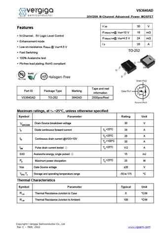
VS3640AD 30V/28A N-Channel Advanced Power MOSFET V DS 30 V Features R DS(on),TYP@ VGS=10 V 16 m N-Channel 5V Logic Level Control R DS(on),TYP@ VGS=4.5 V 24 m Enhancement mode I D 28 A Low on-resistance RDS(on) @ VGS=4.5 V TO-252 Fast Switching 100% Avalanche test Pb-free lead plating; RoHS compliant Tape and reel Part ID Package Type Marking infor
vs3640ac.pdf
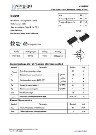
VS3640AC 30V/6A N-Channel Advanced Power MOSFET V DS 30 V Features R DS(on),TYP@ VGS=10 V 19 m N-Channel 5V Logic Level Control R DS(on),TYP@ VGS=4.5 V 27 m Enhancement mode I D 6 A Low on-resistance RDS(on) @ VGS=4.5 V Fast Switching SOT23 Pb-free lead plating; RoHS compliant Part ID Package Type Marking Packing VS3640AC SOT23 VS03 3000pcs/reel Maximu
vs3640db.pdf
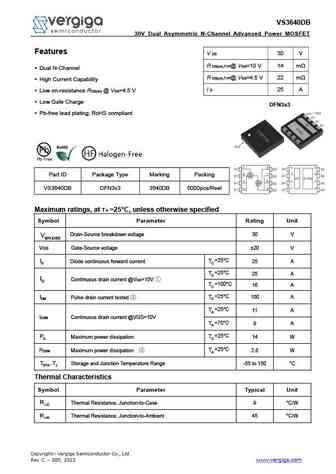
VS3640DB 30V Dual Asymmetric N-Channel Advanced Power MOSFET Features V DS 30 V R DS(on),TYP@ VGS=10 V 14 m Dual N-Channel R DS(on),TYP@ VGS=4.5 V 22 m High Current Capability I D 25 A Low on-resistance RDS(on) @ VGS=4.5 V Low Gate Charge DFN3x3 Pb-free lead plating; RoHS compliant Part ID Package Type Marking Packing VS3640DB DFN3x3 3640DB 5000pcs/Reel
vs3640de.pdf
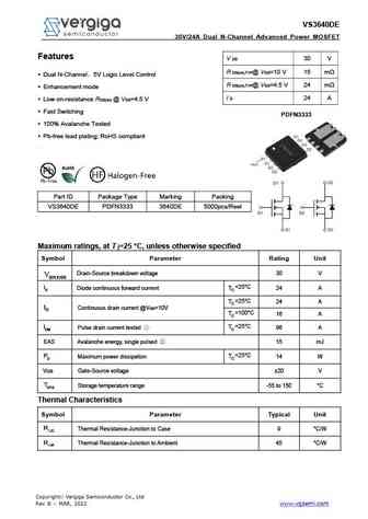
VS3640DE 30V/24A Dual N-Channel Advanced Power MOSFET Features V DS 30 V R DS(on),TYP@ VGS=10 V 15 m Dual N-Channel 5V Logic Level Control R DS(on),TYP@ VGS=4.5 V 24 m Enhancement mode I D 24 A Low on-resistance RDS(on) @ VGS=4.5 V Fast Switching PDFN3333 100% Avalanche Tested Pb-free lead plating; RoHS compliant Part ID Package Type Marking Pa
vs3640bc.pdf
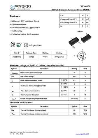
VS3640BC 30V/5A N-Channel Advanced Power MOSFET V DS 30 V Features R DS(on),TYP@ VGS=4.5 V 29 m N-Channel 2.5V Logic Level Control R DS(on),TYP@ VGS=2.5 V 36 m Enhancement mode I D 5 A Low on-resistance RDS(on) @ VGS=4.5 V Fast Switching SOT23 Pb-free lead plating; RoHS compliant Part ID Package Type Marking Packing VS3640BC SOT23 VS06 3000pcs/reel Max
vs4640de.pdf
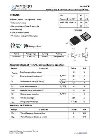
VS4640DE 40V/20A Dual N-Channel Advanced Power MOSFET Features V DS 40 V R DS(on),TYP@ VGS=10 V 26 m Dual N-Channel 5V Logic Level Control R DS(on),TYP@ VGS=4.5 V 39 m Enhancement mode I D 20 A Low on-resistance RDS(on) @ VGS=4.5 V Fast Switching PDFN3333 100% Avalanche Tested Pb-free lead plating; RoHS compliant Part ID Package Type Marking Pa
vs4640ac.pdf
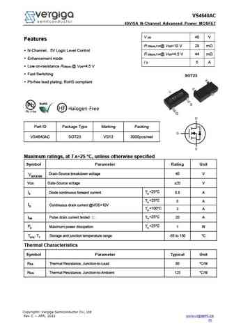
VS4640AC 40V/5A N-Channel Advanced Power MOSFET V DS 40 V Features R DS(on),TYP@ VGS=10 V 29 m N-Channel 5V Logic Level Control R DS(on),TYP@ VGS=4.5 V 44 m Enhancement mode I D 5 A Low on-resistance RDS(on) @ VGS=4.5 V Fast Switching SOT23 Pb-free lead plating; RoHS compliant Part ID Package Type Marking Packing VS4640AC SOT23 VS13 3000pcs/reel Maximu
vs3640at.pdf
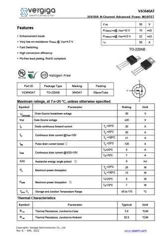
VS3640AT 30V/30A N-Channel Advanced Power MOSFET V DS 30 V Features R DS(on),TYP@ VGS=10 V 15 m Enhancement mode R DS(on),TYP@ VGS=4.5 V 22 m Very low on-resistance RDS(on) @ VGS=4.5 V I D 30 A Fast Switching TO-220AB High conversion efficiency Pb-free lead plating; RoHS compliant Part ID Package Type Marking Packing VS3640AT TO-220AB 3640AT 50pcs/Tube M
vs3640ds.pdf
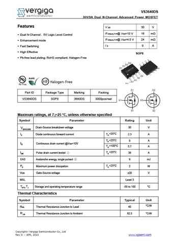
VS3640DS 30V/9A Dual N-Channel Advanced Power MOSFET Features V DS 30 V R DS(on),TYP@ VGS=10 V 16 m Dual N-Channel 5V Logic Level Control R DS(on),TYP@ VGS=4.5 V 24 m Enhancement mode I D 9 A Fast Switching High Effective SOP8 Pb-free lead plating; RoHS compliant; Halogen-Free Part ID Package Type Marking Packing VS3640DS SOP8 3640DS 3000pcs/reel Maxim
vs3640dp.pdf
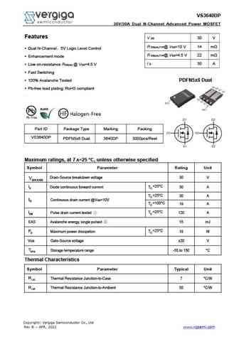
VS3640DP 30V/30A Dual N-Channel Advanced Power MOSFET Features V DS 30 V R DS(on),TYP@ VGS=10 V 14 m Dual N-Channel 5V Logic Level Control R DS(on),TYP@ VGS=4.5 V 22 m Enhancement mode I D 30 A Low on-resistance RDS(on) @ VGS=4.5 V Fast Switching PDFN5x6 Dual 100% Avalanche Tested Pb-free lead plating; RoHS compliant Part ID Package Type Markin
vs3640dp3.pdf
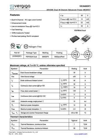
VS3640DP3 30V/30A Dual N-Channel Advanced Power MOSFET Features V DS 30 V R DS(on),TYP@ VGS=10 V 14 m Dual N-Channel 5V Logic Level Control R DS(on),TYP@ VGS=4.5 V 22 m Enhancement mode I D 30 A Low on-resistance RDS(on) @ VGS=4.5 V Fast Switching PDFN5x6 Dual 100% Avalanche Tested Pb-free lead plating; RoHS compliant Part ID Package Type Marki
vs3640ae.pdf
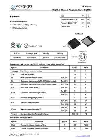
VS3640AE 30V/25A N-Channel Advanced Power MOSFET V DS 30 V Features R DS(on),TYP@ VGS=10 V 13.5 m Enhancement mode R DS(on),TYP@ VGS=4.5 V 23 m Fast Switching and High efficiency I D(Silicon Limited) 25 A 100% Avalanche test PDFN3333 Part ID Package Type Marking Packing VS3640AE PDFN3333 3640AE 5000PCS/Reel Maximum ratings, at TA =25 C, unless otherwise specified
vs3640as.pdf
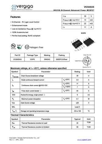
VS3640AS 30V/11A N-Channel Advanced Power MOSFET V DS 30 V Features R DS(on),TYP@ VGS=10 V 14 m N-Channel 5V Logic Level Control R DS(on),TYP@ VGS=4.5 V 22 m Enhancement mode I D 11 A Low on-resistance RDS(on) @ VGS=4.5 V 100% Avalanche test SOP8 Pb-free lead plating; RoHS compliant Part ID Package Type Marking Packing VS3640AS SOP8 3640AS 3000PCS/Reel
hlml6401.pdf
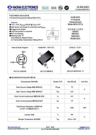
HLML6401 P-Channel MOSFETs -4.3A,-12V P P HLML6401 P-Channel Enhancement-Mode MOS FETs P-Channel Enhancement Features Mode MOS FETs -12V, -4.3A, RDS(ON)=50m @ VGS=-4.5V High dense cell design for extremely low RDS(ON) Rugged and reliable L
aoi66406.pdf
isc N-Channel MOSFET Transistor AOI66406 FEATURES Drain Current I = 60A@ T =25 D C Drain Source Voltage- V =40V(Min) DSS Static Drain-Source On-Resistance R =6.1m (Max) DS(on) 100% avalanche tested Minimum Lot-to-Lot variations for robust device performance and reliable operation DESCRIPTION Designed for use in switch mode power supplies and general purpose
irf640n.pdf
isc N-Channel MOSFET Transistor IRF640N IIRF640N FEATURES Static drain-source on-resistance RDS(on) 150m Enhancement mode Fast Switching Speed 100% avalanche tested Minimum Lot-to-Lot variations for robust device performance and reliable operation DESCRITION Efficient and reliable device for use in a wide variety of applications ABSOLUTE MAXIMUM RATINGS(T
2sa1640.pdf
isc Silicon PNP Power Transistor 2SA1640 DESCRIPTION Collector-Emitter Breakdown Voltage- V = -30V(Min) (BR)CEO Low Collector Saturation Voltage- V = -0.4V(Max)@ (I = -3A, I = -0.1A) CE(sat) C B Minimum Lot-to-Lot variations for robust device performance and reliable operation APPLICATIONS Designed for switching regulator, driver and power switching applications. ABSOLU
2sb1640.pdf
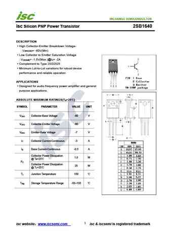
isc Silicon PNP Power Transistor 2SB1640 DESCRIPTION High Collector-Emitter Breakdown Voltage- V = -60V(Min) (BR)CEO Low Collector to Emitter Saturation Voltage V = -1.5V(Max.)@I = -2A CE(sat) C Complement to Type 2SD2525 Minimum Lot-to-Lot variations for robust device performance and reliable operation APPLICATIONS Designed for audio frequency power amplifier and gene
ytf640.pdf
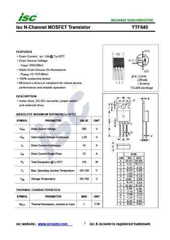
isc N-Channel MOSFET Transistor YTF640 FEATURES Drain Current I = 18A@ T =25 D C Drain Source Voltage V = 200V(Min) DSS Static Drain-Source On-Resistance R =0.18 (Max) DS(on) 100% avalanche tested Minimum Lot-to-Lot variations for robust device performance and reliable operation DESCRIPTION motor drive, DC-DC converter, power switch and solenoid drive. ABSO
irf640ns.pdf
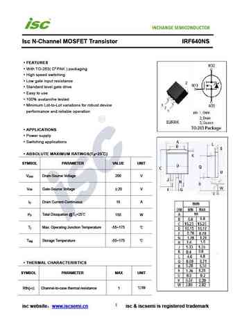
Isc N-Channel MOSFET Transistor IRF640NS FEATURES With TO-263( D PAK ) packaging High speed switching Low gate input resistance Standard level gate drive Easy to use 100% avalanche tested Minimum Lot-to-Lot variations for robust device performance and reliable operation APPLICATIONS Power supply Switching applications ABSOLUTE MAXIMUM RATINGS(T =25 ) a
irlml6402.pdf
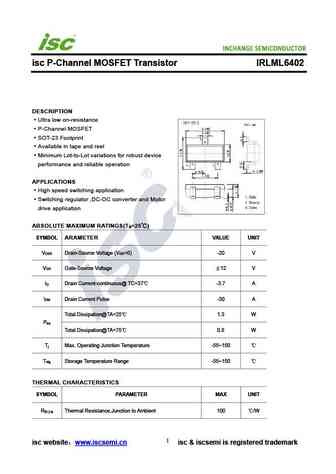
INCHANGE Semiconductor isc P-Channel MOSFET Transistor IRLML6402 DESCRIPTION Ultra low on-resistance P-Channel MOSFET SOT-23 Footprint Available in tape and reel Minimum Lot-to-Lot variations for robust device performance and reliable operation APPLICATIONS High speed switching application Switching regulator ,DC-DC converter and Motor drive application ABSOLUTE MAXIM
2sd640.pdf
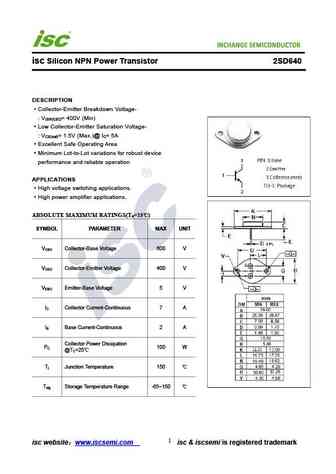
INCHANGE Semiconductor isc Silicon NPN Power Transistor 2SD640 DESCRIPTION Collector-Emitter Breakdown Voltage- V = 400V (Min) (BR)CEO Low Collector-Emitter Saturation Voltage- V = 1.5V (Max.)@ I = 5A CE(sat) C Excellent Safe Operating Area Minimum Lot-to-Lot variations for robust device performance and reliable operation APPLICATIONS High voltage switching applicatio
2sd1640.pdf
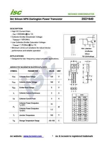
INCHANGE Semiconductor isc Silicon NPN Darlington Power Transistor 2SD1640 DESCRIPTION High DC Current Gain- h = 4000(Min)@ I = 1A FE C Collector-Emitter Breakdown Voltage- V = 100V(Min) (BR)CEO Low Collector-Emitter Saturation Voltage- V = 1.5V(Max)@ I = 1A CE(sat) C Minimum Lot-to-Lot variations for robust device performance and reliable operation APPLICATIONS D
irf640.pdf
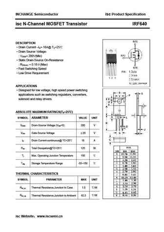
INCHANGE Semiconductor isc Product Specification isc N-Channel MOSFET Transistor IRF640 DESCRIPTION Drain Current ID= 18A@ TC=25 Drain Source Voltage- VDSS= 200V(Min) Static Drain-Source On-Resistance RDS(on) = 0.18 (Max) Fast Switching Speed Low Drive Requirement APPLICATIONS Designed for low voltage, high speed power switching applications suc
aod66406.pdf
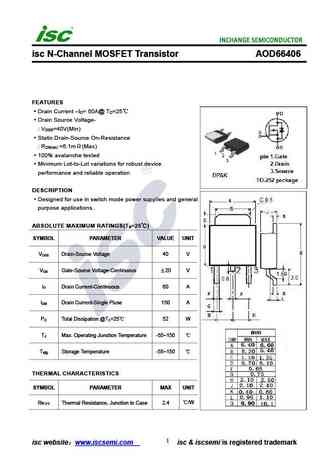
isc N-Channel MOSFET Transistor AOD66406 FEATURES Drain Current I = 60A@ T =25 D C Drain Source Voltage- V =40V(Min) DSS Static Drain-Source On-Resistance R =6.1m (Max) DS(on) 100% avalanche tested Minimum Lot-to-Lot variations for robust device performance and reliable operation DESCRIPTION Designed for use in switch mode power supplies and general purpose
2sc3640.pdf
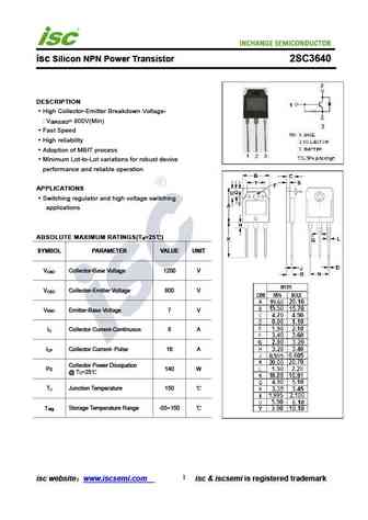
isc Silicon NPN Power Transistor 2SC3640 DESCRIPTION High Collector-Emitter Breakdown Voltage- V = 800V(Min) (BR)CEO Fast Speed High reliability Adoption of MBIT process Minimum Lot-to-Lot variations for robust device performance and reliable operation APPLICATIONS Switching regulator and high voltage switching applications ABSOLUTE MAXIMUM RATINGS(T =25 ) a SYMBO
irf640nl.pdf
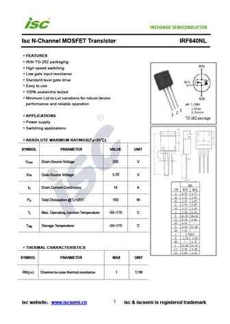
Isc N-Channel MOSFET Transistor IRF640NL FEATURES With TO-262 packaging High speed switching Low gate input resistance Standard level gate drive Easy to use 100% avalanche tested Minimum Lot-to-Lot variations for robust device performance and reliable operation APPLICATIONS Power supply Switching applications ABSOLUTE MAXIMUM RATINGS(T =25 ) a SYMBOL PAR
ipd640n06l.pdf
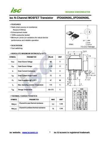
isc N-Channel MOSFET Transistor IPD640N06L,IIPD640N06L FEATURES Static drain-source on-resistance RDS(on) 64m Enhancement mode 100% avalanche tested Minimum Lot-to-Lot variations for robust device performance and reliable operation DESCRITION Fast switching ABSOLUTE MAXIMUM RATINGS(T =25 ) a SYMBOL PARAMETER VALUE UNIT V Drain-Source Voltage 60 V DSS V Ga
Другие IGBT... 80N08TR, 8205A, 8205B, G3205, G1010, G3710, 5N20A, 630A, IRFZ44N, 18N20, 18N20A, 2N25, 3N25, 740, 840, 16N50F, 13N50F
Параметры MOSFET. Взаимосвязь и компромиссы
History: 5N60L-K08-5060-R | AON6704A
🌐 : EN ES РУ

Список транзисторов
Обновления
MOSFET: CS95118 | CS85105A | CS75N45 | CS72N12 | CS55N50 | CS48N75A | CS40N27 | MSQ60P04D | MSQ40P07D | MSQ30P40D | MSQ30P15 | MSQ30P07D | MSQ100N03D | MSHM60P14 | MSHM40N085 | MSHM30N46
Popular searches
irfz44n | irf3205 | irfz44n datasheet | 2n4401 | bc547 transistor | bd139 | 2n4401 datasheet | irf640