3N25. Аналоги и основные параметры
Наименование производителя: 3N25
Тип транзистора: MOSFET
Полярность: N
Предельные значения
Pd ⓘ
- Максимальная рассеиваемая мощность: 50 W
|Vds|ⓘ - Максимально допустимое напряжение сток-исток: 250 V
|Vgs|ⓘ - Максимально допустимое напряжение затвор-исток: 20 V
|Id| ⓘ - Максимально допустимый постоянный ток стока: 3 A
Tj ⓘ - Максимальная температура канала: 150 °C
Электрические характеристики
tr ⓘ -
Время нарастания: 25.3 ns
Cossⓘ - Выходная емкость: 27 pf
RDSonⓘ - Сопротивление сток-исток открытого транзистора: 1.7 Ohm
Тип корпуса: TO251
TO252
- подборⓘ MOSFET транзистора по параметрам
3N25 даташит
..1. Size:1752K goford
3n25.pdf 
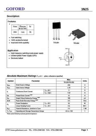
GOFORD 3N25 Description Features - VDSS RDS(ON) ID @ 10V (typ) 3A 250V 1.4 Fast switching 100% avalanche tested Improved dv/dt capability TO-251 TO-252 Application High frequency switching mode power supply Uninterruptible Power Supply (UPS) Electronic ballast Absolute Maximum Ratings TC=25 unless otherwise specified Max.
0.2. Size:219K motorola
mtd3n25e.pdf 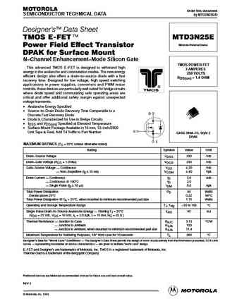
MOTOROLA Order this document SEMICONDUCTOR TECHNICAL DATA by MTD3N25E/D Designer's Data Sheet TMOS E-FET. MTD3N25E Motorola Preferred Device Power Field Effect Transistor DPAK for Surface Mount N Channel Enhancement Mode Silicon Gate TMOS POWER FET This advanced TMOS E FET is designed to withstand high 3 AMPERES energy in the avalanche and commutation modes. The new en
0.3. Size:253K motorola
mtd3n25erev2x.pdf 
MOTOROLA Order this document SEMICONDUCTOR TECHNICAL DATA by MTD3N25E/D Designer's Data Sheet TMOS E-FET. MTD3N25E Motorola Preferred Device Power Field Effect Transistor DPAK for Surface Mount N Channel Enhancement Mode Silicon Gate TMOS POWER FET This advanced TMOS E FET is designed to withstand high 3 AMPERES energy in the avalanche and commutation modes. The new en
0.4. Size:181K motorola
mtp3n25e.pdf 
MOTOROLA Order this document SEMICONDUCTOR TECHNICAL DATA by MTP3N25E/D Designer's Data Sheet MTP3N25E TMOS E-FET. Motorola Preferred Device Power Field Effect Transistor N Channel Enhancement Mode Silicon Gate TMOS POWER FET This advanced TMOS E FET is designed to withstand high 3.0 AMPERES energy in the avalanche and commutation modes. The new energy 250 VOLTS effic
0.5. Size:95K motorola
mtw23n25e.pdf 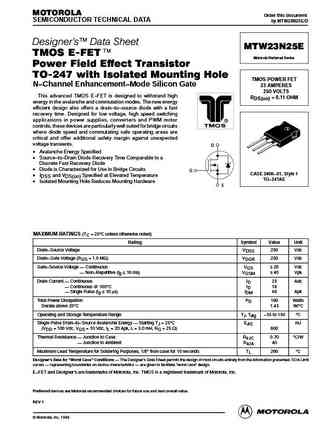
MOTOROLA Order this document SEMICONDUCTOR TECHNICAL DATA by MTW23N25E/D Designer's Data Sheet MTW23N25E TMOS E-FET. Motorola Preferred Device Power Field Effect Transistor TO-247 with Isolated Mounting Hole TMOS POWER FET N Channel Enhancement Mode Silicon Gate 23 AMPERES 250 VOLTS This advanced TMOS E FET is designed to withstand high RDS(on) = 0.11 OHM energy in
0.6. Size:208K motorola
mtp3n25erev2.pdf 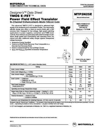
MOTOROLA Order this document SEMICONDUCTOR TECHNICAL DATA by MTP3N25E/D Designer's Data Sheet MTP3N25E TMOS E-FET. Motorola Preferred Device Power Field Effect Transistor N Channel Enhancement Mode Silicon Gate TMOS POWER FET This advanced TMOS E FET is designed to withstand high 3.0 AMPERES energy in the avalanche and commutation modes. The new energy 250 VOLTS effic
0.7. Size:152K motorola
mtw23n25erev2.pdf 
MOTOROLA Order this document SEMICONDUCTOR TECHNICAL DATA by MTW23N25E/D Designer's Data Sheet MTW23N25E TMOS E-FET. Motorola Preferred Device Power Field Effect Transistor TO-247 with Isolated Mounting Hole TMOS POWER FET N Channel Enhancement Mode Silicon Gate 23 AMPERES 250 VOLTS This advanced TMOS E FET is designed to withstand high RDS(on) = 0.11 OHM energy in
0.8. Size:172K st
std3n25.pdf 
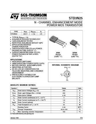
STD3N25 N - CHANNEL ENHANCEMENT MODE POWER MOS TRANSISTOR TYPE V R I DSS DS(on) D STD3N25 250 V
0.9. Size:885K fairchild semi
fdi33n25.pdf 
May 2006 TM UniFET FDB33N25 / FDI33N25 250V N-Channel MOSFET Features Description 33A, 250V, RDS(on) = 0.094 @VGS = 10 V These N-Channel enhancement mode power field effect transistors are produced using Fairchild s proprietary, planar Low gate charge ( typical 36.8 nC) stripe, DMOS technology. Low Crss ( typical 39 pF) This advanced technology has been especially
0.10. Size:621K fairchild semi
fqb3n25tm fqi3n25tu.pdf 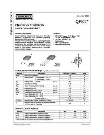
November 2000 TM QFET QFET QFET QFET FQB3N25 / FQI3N25 250V N-Channel MOSFET General Description Features These N-Channel enhancement mode power field effect 2.8A, 250V, RDS(on) = 2.2 @VGS = 10 V transistors are produced using Fairchild s proprietary, Low gate charge ( typical 4.0 nC) planar stripe, DMOS technology. Low Crss ( typical 4.7 pF) This advanced technolo
0.11. Size:612K fairchild semi
fqp3n25.pdf 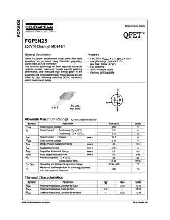
November 2000 TM QFET QFET QFET QFET FQP3N25 250V N-Channel MOSFET General Description Features These N-Channel enhancement mode power field effect 2.8A, 250V, RDS(on) = 2.2 @VGS = 10 V transistors are produced using Fairchild s proprietary, Low gate charge ( typical 4.0 nC) planar stripe, DMOS technology. Low Crss ( typical 4.7 pF) This advanced technology has bee
0.12. Size:1205K fairchild semi
fdp33n25 fdpf33n25t.pdf 
October TM UniFET FDP33N25 / FDPF33N25T 250V N-Channel MOSFET Features Description 33A, 250V, RDS(on) = 0.094 @VGS = 10 V These N-Channel enhancement mode power field effect Low gate charge ( typical 36.8 nC) transistors are produced using Fairchild s proprietary, planar Low Crss ( typical 39 pF) stripe, DMOS technology. Fast switching This advanced technolog
0.13. Size:643K fairchild semi
fda33n25.pdf 
September 2007 UniFETTM FDA33N25 tm N-Channel MOSFET 250V, 33A, 0.094 Features Description RDS(on) = 0.088 ( Typ.)@ VGS = 10V, ID = 16.5A These N-Channel enhancement mode power field effect transis- tors are produced using Fairchild s proprietary, planar stripe, Low gate charge ( Typ. 36nC) DMOS technology. Low Crss ( Typ. 35pF) This advance technology has been
0.14. Size:448K fairchild semi
fdpf33n25trdtu.pdf 
August 2014 FDPF33N25T N-Channel UniFETTM MOSFET 250 V, 33 A, 94 m Features Description UniFETTM MOSFET is Fairchild Semiconductor s high voltage RDS(on) = 94 m (Max.) @ VGS = 10 V, ID = 16.5 A MOSFET family based on planar stripe and DMOS technology. Low Gate Charge (Typ. 36.8 nC) This MOSFET is tailored to reduce on-state resistance, and to Low Crss (Typ. 39 pF) p
0.15. Size:916K fairchild semi
fdb33n25 fdi33n25.pdf 
May 2006 TM UniFET FDB33N25 / FDI33N25 250V N-Channel MOSFET Features Description 33A, 250V, RDS(on) = 0.094 @VGS = 10 V These N-Channel enhancement mode power field effect transistors are produced using Fairchild s proprietary, planar Low gate charge ( typical 36.8 nC) stripe, DMOS technology. Low Crss ( typical 39 pF) This advanced technology has been especially
0.16. Size:724K fairchild semi
fqpf3n25.pdf 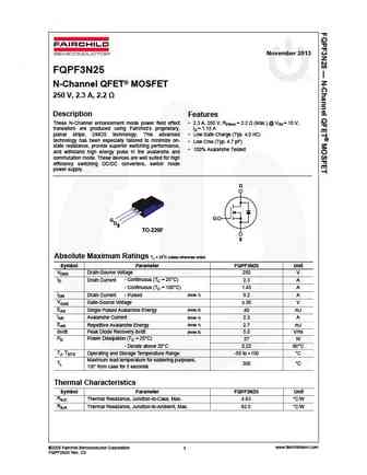
November 2013 FQPF3N25 N-Channel QFET MOSFET 250 V, 2.3 A, 2.2 Description Features These N-Channel enhancement mode power field effect 2.3 A, 250 V, RDS(on) = 2.2 (Max.) @ VGS = 10 V, transistors are produced using Fairchild s proprietary, ID = 1.15 A planar stripe, DMOS technology. This advanced Low Gate Charge (Typ. 4.0 nC) technology has been especially tailored
0.17. Size:534K onsemi
fdb33n25.pdf 
Is Now Part of To learn more about ON Semiconductor, please visit our website at www.onsemi.com Please note As part of the Fairchild Semiconductor integration, some of the Fairchild orderable part numbers will need to change in order to meet ON Semiconductor s system requirements. Since the ON Semiconductor product management systems do not have the ability to manage part nomenclatur
0.18. Size:526K onsemi
fdpf33n25t.pdf 
Is Now Part of To learn more about ON Semiconductor, please visit our website at www.onsemi.com Please note As part of the Fairchild Semiconductor integration, some of the Fairchild orderable part numbers will need to change in order to meet ON Semiconductor s system requirements. Since the ON Semiconductor product management systems do not have the ability to manage part nomenclatur
0.19. Size:478K onsemi
fdp33n25.pdf 
Is Now Part of To learn more about ON Semiconductor, please visit our website at www.onsemi.com Please note As part of the Fairchild Semiconductor integration, some of the Fairchild orderable part numbers will need to change in order to meet ON Semiconductor s system requirements. Since the ON Semiconductor product management systems do not have the ability to manage part nomenclatur
0.20. Size:892K onsemi
fqpf3n25.pdf 
Is Now Part of To learn more about ON Semiconductor, please visit our website at www.onsemi.com Please note As part of the Fairchild Semiconductor integration, some of the Fairchild orderable part numbers will need to change in order to meet ON Semiconductor s system requirements. Since the ON Semiconductor product management systems do not have the ability to manage part nomenclatur
0.21. Size:156K utc
uf3n25.pdf 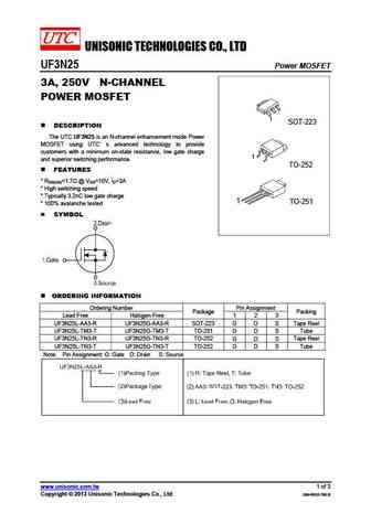
UNISONIC TECHNOLOGIES CO., LTD UF3N25 Power MOSFET 3A, 250V N-CHANNEL POWER MOSFET 1 SOT-223 DESCRIPTION The UTC UF3N25 is an N-channel enhancement mode Power MOSFET using UTC s advanced technology to provide customers with a minimum on-state resistance, low gate charge 1 and superior switching performance. TO-252 FEATURES * RDS(ON)
0.22. Size:512K jilin sino
jcs33n25ct.pdf 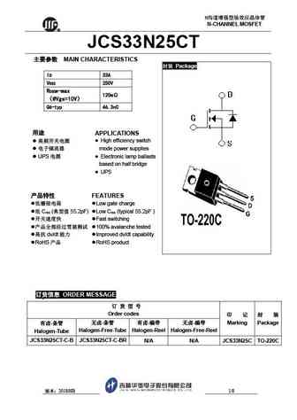
N N-CHANNEL MOSFET R JCS33N25CT MAIN CHARACTERISTICS Package ID 33A VDSS 250V RDSON-max 120m @Vgs=10V QG-typ 46.3nC APPLICATIONS High efficiency switch mode power supplies UPS Electronic lamp ballasts based on half bridge UPS
0.23. Size:952K blue-rocket-elect
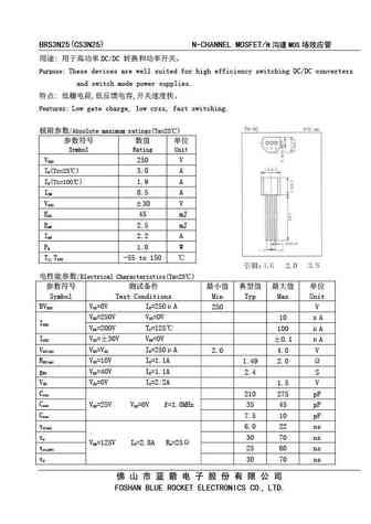
bri3n25.pdf 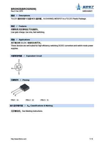
BRI3N25(BRCS3N25I) Rev.C Feb.-2015 DATA SHEET / Descriptions TO-251 N MOS N-CHANNEL MOSFET in a TO-251 Plastic Package. / Features , , Low gate charge, low crss, fast switching. / Applications DC/DC These devices are well suited for high ef
0.25. Size:1102K blue-rocket-elect
brd3n25.pdf 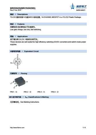
BRD3N25(BRCS3N25D) Rev.C Feb.-2015 DATA SHEET / Descriptions TO-252 N MOS N-CHANNEL MOSFET in a TO-252 Plastic Package. / Features , , Low gate charge, low crss, fast switching. / Applications DC/DC These devices are well suited for high
0.26. Size:105K kexin
kxu03n25.pdf 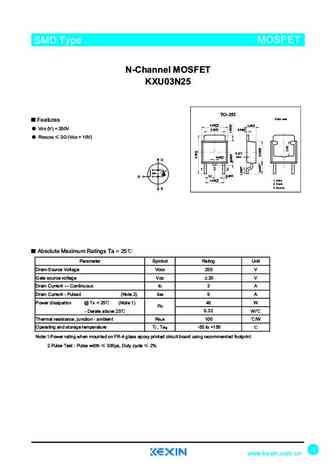
SMD Type MOSFET N-Channel MOSFET KXU03N25 TO-252 Unit mm Features 6.50+0.15 2.30+0.1 -0.15 -0.1 +0.2 +0.8 VDS (V) = 250V 5.30-0.2 0.50-0.7 RDS(ON) 2 (VGS = 10V) 0.127 0.80+0.1 max -0.1 2 1 3 2.3 0.60+0.1 -0.1 +0.15 1. Gate 4.60-0.15 2. Drain 3. Source Absolute Maximum Ratings Ta = 25 Parameter Symbol Rating Unit Drain-Source Voltage VDSS 250
0.27. Size:1197K belling
bl13n25-p bl13n25-a bl13n25-u bl13n25-d.pdf 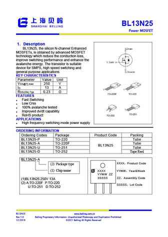
BL13N25 Power MOSFET 1 Description Step-Down Converter BL13N25, the silicon N-channel Enhanced , MOSFETs, is obtained by advanced MOSFET technology which reduce the conduction loss, improve switching performance and enhance the avalanche energy. The transistor is suitable device for SMPS, high speed switching and general purpose applications. KEY CHARACTERISTICS Pa
0.28. Size:1198K belling
bl13n25l-p bl13n25l-a bl13n25l-u bl13n25l-d.pdf 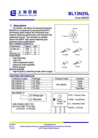
BL13N25L Power MOSFET 1 Description Step-Down Converter BL13N25L, the silicon N-channel Enhanced , MOSFETs, is obtained by advanced MOSFET technology which reduce the conduction loss, improve switching performance and enhance the avalanche energy. The transistor is suitable device for SMPS, high speed switching and general purpose applications. KEY CHARACTERISTICS
0.29. Size:862K belling
bl33n25-p bl33n25-a.pdf 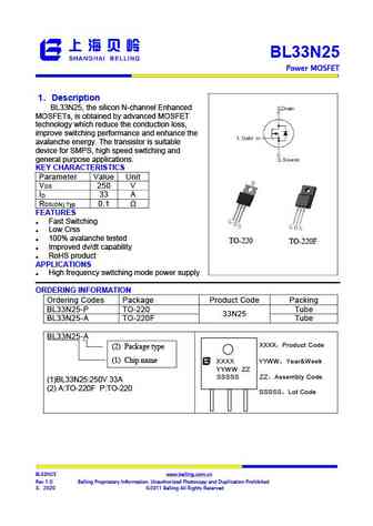
BL33N25 Power MOSFET 1 Description Step-Down Converter BL33N25, the silicon N-channel Enhanced , MOSFETs, is obtained by advanced MOSFET technology which reduce the conduction loss, improve switching performance and enhance the avalanche energy. The transistor is suitable device for SMPS, high speed switching and general purpose applications. KEY CHARACTERISTICS Pa
0.30. Size:887K cn hmsemi
hm3n25i.pdf 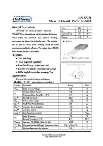
HM3N25I Silicon N-Channel Power MOSFET General Description VDSS 250 V HM3N25I, the silicon N-channel Enhanced ID 3.0 A PD(TC=25 ) 30 W VDMOSFETs, is obtained by the self-aligned planar Technology RDS(ON) 1.0 which reduce the conduction loss, improve switching performance and enhance the avalanche energy. The transistor can be used in various power switching circuit
0.31. Size:561K cn minos
md33n25.pdf 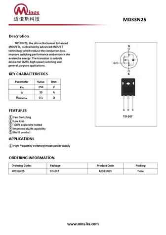
Description MD33N25, the silicon N-channel Enhanced MOSFETs, is obtained by advanced MOSFET technology which reduce the conduction loss, improve switching performance and enhance the avalanche energy. The transistor is suitable device for SMPS, high speed switching and general purpose applications. KEY CHARACTERISTICS Parameter Value Unit V 250 V DS I 33 A D R 0.1 DS(ON).Typ
0.32. Size:281K inchange semiconductor
fdi33n25.pdf 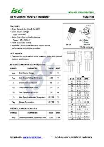
isc N-Channel MOSFET Transistor FDI33N25 FEATURES Drain Current I = 33A@ T =25 D C Drain Source Voltage- V =250V(Min) DSS Static Drain-Source On-Resistance R = 94m (Max) DS(on) 100% avalanche tested Minimum Lot-to-Lot variations for robust device performance and reliable operation DESCRIPTION Designed for use in switch mode power su pplies and general purpo
0.33. Size:288K inchange semiconductor
fdp33n25.pdf 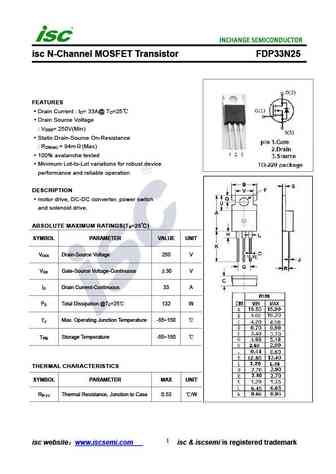
isc N-Channel MOSFET Transistor FDP33N25 FEATURES Drain Current I = 33A@ T =25 D C Drain Source Voltage V = 250V(Min) DSS Static Drain-Source On-Resistance R = 94m (Max) DS(on) 100% avalanche tested Minimum Lot-to-Lot variations for robust device performance and reliable operation DESCRIPTION motor drive, DC-DC converter, power switch and solenoid drive. AB
Другие MOSFET... G1010
, G3710
, 5N20A
, 630A
, 640
, 18N20
, 18N20A
, 2N25
, IRF540N
, 740
, 840
, 16N50F
, 13N50F
, 20N50
, 5N60F
, 7N60F
, 8N60A
.
History: SST201
| 840
| 13N50F