16N50F. Аналоги и основные параметры
Наименование производителя: 16N50F
Тип транзистора: MOSFET
Полярность: N
Предельные значения
Pd ⓘ - Максимальная рассеиваемая мощность: 38.5 W
|Vds|ⓘ - Максимально допустимое напряжение сток-исток: 500 V
|Vgs|ⓘ - Максимально допустимое напряжение затвор-исток: 30 V
|Id| ⓘ - Максимально допустимый постоянный ток стока: 16 A
Tj ⓘ - Максимальная температура канала: 150 °C
Электрические характеристики
tr ⓘ - Время нарастания: 170 ns
Cossⓘ - Выходная емкость: 350 pf
RDSonⓘ - Сопротивление сток-исток открытого транзистора: 0.38 Ohm
Тип корпуса: TO220F
Аналог (замена) для 16N50F
- подборⓘ MOSFET транзистора по параметрам
16N50F даташит
kf16n50f.pdf
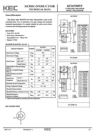
KF16N50P/F SEMICONDUCTOR N CHANNEL MOS FIELD TECHNICAL DATA EFFECT TRANSISTOR General Description KF16N50P A This planar stripe MOSFET has better characteristics, such as fast O C switching time, low on resistance, low gate charge and excellent F avalanche characteristics. It is mainly suitable for active power factor E DIM MILLIMETERS G correction and switching mode power supp
fir16n50fg.pdf
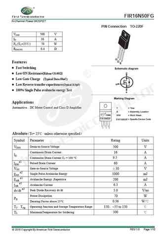
FIR16N50FG CREAT BY ART N-Channel Power MOSFET PIN Connection TO-220F VDSS 500 V ID 16 A PD (TC=25 ) 70 W RDS(ON) 0.4 G D S Features Fast Switching g Schematic dia ram D Low ON Resistance(Rdson 0.40 ) Low Gate Charge (Typical Data 50nC) G Low Reverse transfer capacitances(Typical 25.5pF) 100% Single Pulse avalanche energy Test S Marking Diagram Ap
hm16n50 hm16n50f.pdf
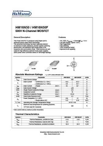
HM16N50 / HM16N50F 500V N-Channel MOSFET General Description Features This Power MOSFET is produced using Maple semi s - 16A, 500V, RDS(on)typ. = 305m @VGS = 10 V advanced planar stripe DMOS technology. - Low gate charge ( typical 52nC) This advanced technology has been especially tailored - High ruggedness to minimize on-state resistance, provide superior switching - Fast switching p
Другие MOSFET... 630A , 640 , 18N20 , 18N20A , 2N25 , 3N25 , 740 , 840 , IRFP460 , 13N50F , 20N50 , 5N60F , 7N60F , 8N60A , 8N60AF , 10N60F , 12N60F .
History: 10N65A
History: 10N65A
🌐 : EN ES РУ

Список транзисторов
Обновления
MOSFET: ASD80R750E | ASD70R950E | ASD70R600E | ASD70R380E | ASD65R850E | ASD65R550E | ASD65R350E | ASD65R300E | ASD65R280E | ASD65R270E | ASD60R330E | ASD60R280E | ASB80R750E | ASB70R380E | ASB65R300E | ASB65R220E
Popular searches
irf640 | irf840 | irf740 | c945 transistor | irf640n | 2n3904 | bc547 datasheet | k3797 mosfet