SD201DC. Аналоги и основные параметры
Наименование производителя: SD201DC
Тип транзистора: MOSFET
Полярность: N
Предельные значения
Pd ⓘ
- Максимальная рассеиваемая мощность: 0.36 W
|Vds|ⓘ - Максимально допустимое напряжение сток-исток: 25 V
|Vgs|ⓘ - Максимально допустимое напряжение затвор-исток: 20 V
|Id| ⓘ - Максимально допустимый постоянный ток стока: 0.05 A
Tj ⓘ - Максимальная температура канала: 125 °C
Электрические характеристики
Cossⓘ - Выходная емкость: 1 pf
RDSonⓘ - Сопротивление сток-исток открытого транзистора: 70 Ohm
Тип корпуса: TO-52
Аналог (замена) для SD201DC
- подборⓘ MOSFET транзистора по параметрам
SD201DC даташит
..1. Size:26K calogic
sd200dc sd201dc sd202dc sd203dc sstsd201 sstsd203.pdf 
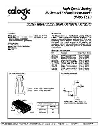
High-Speed Analog N-Channel Enhancement-Mode LLC DMOS FETS SD200 / SD201 / SD202 / SD203 / SSTSD201 / SSTSD203 FEATURES DESCRIPTION High gain . . . . . . . . . . . . . . . . . . . . . 8.0 dB min @ 1 GHz The SD200 series is manufactured utilizing Calogic s Low Noise. . . . . . . . . . . . . . . . . . . . . 5.0 dB max @ 1 GHz proprietary DMOS design and processing techniques
9.2. Size:126K toshiba
2sd2012.pdf 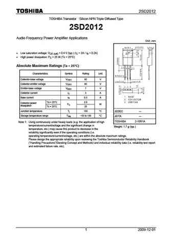
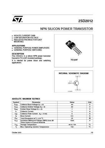
2SD2012 TOSHIBA Transistor Silicon NPN Triple Diffused Type 2SD2012 Audio Frequency Power Amplifier Applications Unit mm Low saturation voltage VCE (sat) = 0.4 V (typ.) (IC = 2A / IB = 0.2A) High power dissipation PC = 25 W (Tc = 25 C) Absolute Maximum Ratings (Ta = 25 C) Characteristics Symbol Rating Unit Collector-base voltage VCBO 60 V Collector-emitter voltage
9.3. Size:46K fairchild semi
ksd2012.pdf 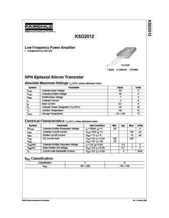
KSD2012 Low Frequency Power Amplifier Complement to KSB1366 TO-220F 1 1.Base 2.Collector 3.Emitter NPN Epitaxial Silicon Transistor Absolute Maximum Ratings TC=25 C unless otherwise noted Symbol Parameter Value Units VCBO Collector-Base Voltage 60 V VCEO Collector-Emitter Voltage 60 V VEBO Emitter-Base Voltage 7 V IC Collector Current 3 A IB Base Current 0.3 A PC Collector
9.4. Size:365K samsung
ssd2019.pdf 
I I I I 8 SOIC FEATURES 8 S1 1 D1 G1 2 7 D1 3 6 S2 D2 Lower RDS(ON) 5 G2 4 D2 Improved Inductive Ruggedness Top View Fast Swtching Times S1 Low Input Capacitance Extended Safe Operating Area Improved High Temperature Reliability G1 Product Summary Part Number BVdss Rds(on) ID SSD2019 -20V 0.11 -3.4A D1 D1 P-Channel MOSFET Absolute Maxim
9.5. Size:366K samsung
ssd2017.pdf 
I I I I 8 SOIC FEATURES 8 S1 1 D1 G1 2 7 D1 3 6 S2 D2 Lower RDS(ON) 5 G2 4 D2 Improved Inductive Ruggedness Top View Fast Swtching Times D1 D1 Low Input Capacitance Extended Safe Operating Area Improved High Temperature Reliability G1 Product Summary Part Number BVdss Rds(on) ID S1 SSD2017 20V 0.05 5.0A N -Channel MOSFET Absolute Maximum
9.6. Size:347K samsung
ssd2011.pdf 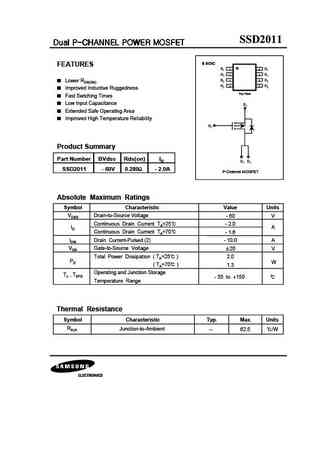
I I I I 8 SOIC FEATURES 8 S1 1 D1 G1 2 7 D1 3 6 S2 D2 Lower RDS(ON) 5 G2 4 D2 Improved Inductive Ruggedness Top View Fast Swtching Times Low Input Capacitance S1 Extended Safe Operating Area Improved High Temperature Reliability G1 Product Summary Part Number BVdss Rds(on) ID D1 D1 SSD2011 - 60V 0.280 - 2.0A P-Channel MOSFET Absolute Ma
9.7. Size:366K rohm
rsd201n10.pdf 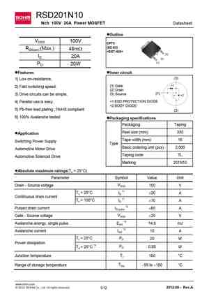
RSD201N10 Nch 100V 20A Power MOSFET Datasheet lOutline VDSS 100V CPT3 (SC-63) RDS(on) (Max.) 46mW (3) ID 20A (2) (1) PD 20W lFeatures lInner circuit (3) 1) Low on-resistance. *1 (1) Gate 2) Fast switching speed. (2) Drain (1) (3) Source 3) Drive circuits can be simple. *2 *1 ESD PROTECTION DIODE 4) Parallel use is easy. *2 BODY DIODE 5) Pb-f
9.8. Size:892K rohm
rsd201n10fra.pdf 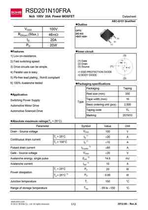
RSD201N10FRA Nch 100V 20A Power MOSFET Datasheet AEC-Q101 Qualified lOutline VDSS 100V CPT3 (SC-63) RDS(on) (Max.) 46mW (3) ID 20A (2) (1) PD 20W lFeatures lInner circuit (3) 1) Low on-resistance. *1 (1) Gate 2) Fast switching speed. (2) Drain (1) (3) Source 3) Drive circuits can be simple. *2 *1 ESD PROTECTION DIODE 4) Parallel use is easy.
9.9. Size:78K panasonic
2sd2018.pdf 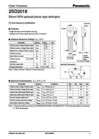
Power Transistors 2SD2018 Silicon NPN epitaxial planar type darlington For low-frequency amplification Unit mm 8.0+0.5 0.1 3.2 0.2 3.16 0.1 Features High forward current transfer ratio hFE Built-in 60 V Zener diode between base to collector Absolute Maximum Ratings Ta = 25 C Parameter Symbol Rating Unit Collector-base voltage (Emitter open) VCBO 60+25 V
9.10. Size:32K hitachi
2sd2019.pdf 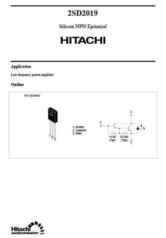
2SD2019 Silicon NPN Epitaxial Application Low frequency power amplifier Outline TO-126 MOD 2 3 1. Emitter ID 2. Collector 3. Base 1 15 k 0.5 k 2 3 (Typ) (Typ) 1 2SD2019 Absolute Maximum Ratings (Ta = 25 C) Item Symbol Ratings Unit Collector to base voltage VCBO 150 V Collector to emitter voltage VCEO 80 V Emitter to base voltage VEBO 8V Collector current IC 1.5 A
9.11. Size:949K jiangsu
2sd2012.pdf 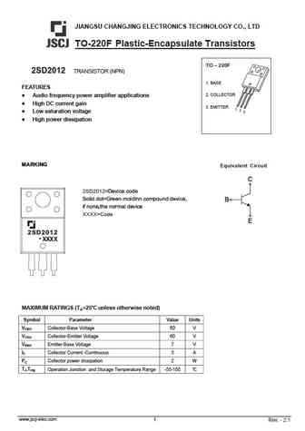
JIANGSU CHANGJING ELECTRONICS TECHNOLOGY CO., LTD TO-220F Plastic-Encapsulate Transistors TO 220F 2SD2012 TRANSISTOR (NPN) 1. BASE FEATURES 2. COLLECTOR Audio frequency power amplifier applications High DC current gain 3. EMITTER 1 2 Low saturation voltage 3 High power dissipation Equivalent Circuit 2SD2012=Device code Solid dot=Green moldinn compound de
9.12. Size:72K jmnic
2sd2015.pdf 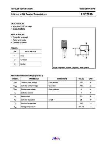
Product Specification www.jmnic.com Silicon NPN Power Transistors 2SD2015 DESCRIPTION With TO-220F package DARLINGTON APPLICATIONS Driver for solenoid Relay and motor General purpose PINNING PIN DESCRIPTION 1 Base 2 Collector 3 Emitter Fig.1 simplified outline (TO-220F) and symbol Absolute maximum ratings (Ta=25 ) SYMBOL PARAMETER CONDITIONS VALUE UNIT
9.13. Size:21K sanken-ele
2sd2016.pdf 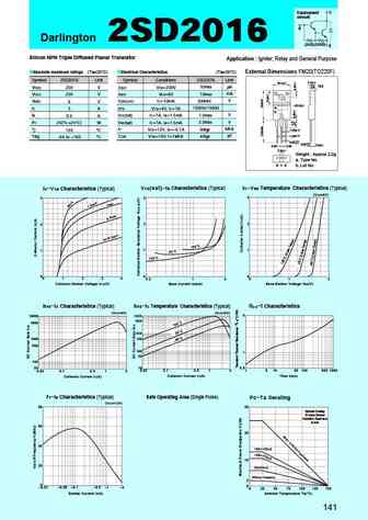
C Equivalent circuit B Darlington 2SD2016 (2k ) (200 ) E Silicon NPN Triple Diffused Planar Transistor Application Igniter, Relay and General Purpose Absolute maximum ratings (Ta=25 C) Electrical Characteristics (Ta=25 C) External Dimensions FM20(TO220F) Symbol 2SD2016 Unit Symbol Conditions 2SD2016 Unit 0.2 4.2 0.2 10.1 c0.5 2.8 A VCBO 200 V ICBO VCB=200V 10ma
9.14. Size:26K sanken-ele
2sd2015.pdf 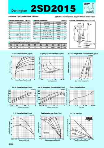
Equivalent C circuit B Darlington 2SD2015 (3k ) (500 ) E Silicon NPN Triple Diffused Planar Transistor Application Driver for Solenoid, Relay and Motor and General Purpose Absolute maximum ratings (Ta=25 C) Electrical Characteristics (Ta=25 C) External Dimensions FM20(TO220F) Symbol Conditions 2SD2015 Symbol 2SD2015 Unit Unit 0.2 4.2 0.2 10.1 c0.5 2.8 ICBO VCB=150V
9.15. Size:25K sanken-ele
2sd2017.pdf 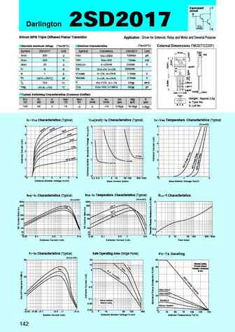
Equivalent C circuit B Darlington 2SD2017 (4k ) E Silicon NPN Triple Diffused Planar Transistor Application Driver for Solenoid, Relay and Motor and General Purpose (Ta=25 C) Absolute maximum ratings (Ta=25 C) Electrical Characteristics External Dimensions FM20(TO220F) Symbol 2SD2017 Symbol Conditions 2SD2017 Unit Unit 0.2 4.2 0.2 10.1 c0.5 2.8 VCBO 300 ICBO VCB=300
9.16. Size:26K sanken-ele
2sd2014.pdf 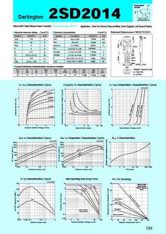
Equivalent C circuit B Darlington 2SD2014 (3k ) (200 ) E Silicon NPN Triple Diffused Planar Transistor (Complement to type 2SB1257) Application Driver for Solenoid, Relay and Motor, Series Regulator, and General Purpose Absolute maximum ratings (Ta=25 C) Electrical Characteristics (Ta=25 C) External Dimensions FM20(TO220F) Symbol 2SD2014 Symbol Conditions 2SD2014 Unit 4.2 Uni
9.17. Size:1808K winsok
wsd2018adn22.pdf 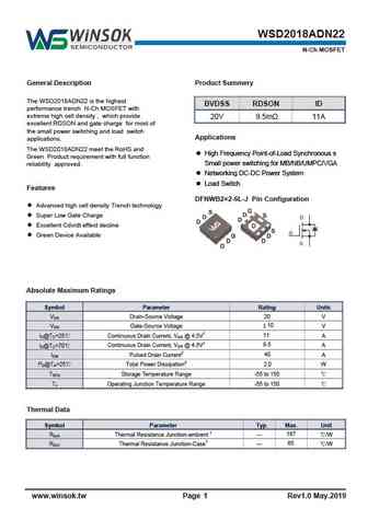
WSD2018ADN22 N-Ch MOSFET General Description Product Summery The WSD2018ADN22 is the highest BVDSS RDSON ID performance trench N-Ch MOSFET with extreme high cell density , which provide 20V 9.5m 11A excellent RDSON and gate charge for most of the small power switching and load switch Applications applications. The WSD2018ADN22 meet the RoHS and High Frequency Point-of-Load S
9.18. Size:2643K winsok
wsd2018dn22.pdf 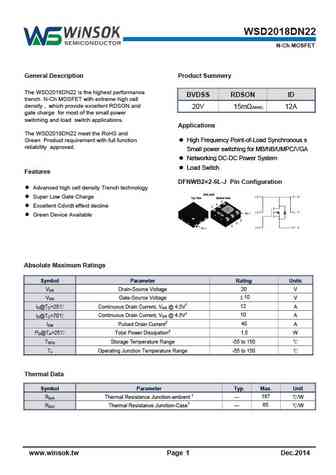
WSD2018DN22 N-Ch MOSFET General Description Product Summery The WSD2018DN22 is the highest performance BVDSS RDSON ID trench N-Ch MOSFET with extreme high cell density , which provide excellent RDSON and 20V 15m (MAX) 12A gate charge for most of the small power switching and load switch applications. Applications The WSD2018DN22 meet the RoHS and Green Product requirement
9.19. Size:1316K winsok
wsd2012dn25.pdf 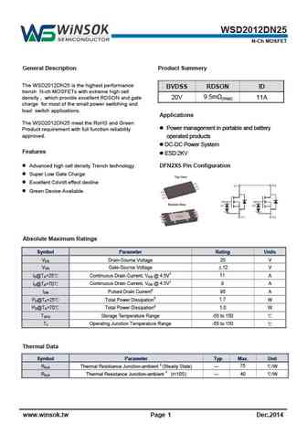
WSD2012DN25 N-Ch MOSFET General Description Product Summery The WSD2012DN25 is the highest performance BVDSS RDSON ID trench N-ch MOSFETs with extreme high cell 9.5m (max) density , which provide excellent RDSON and gate 20V 11A charge for most of the small power switching and load switch applications. Applications The WSD2012DN25 meet the RoHS and Green Power management
9.20. Size:1786K winsok
wsd2018bdn22.pdf 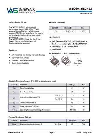
WSD2018BDN22 N-Ch MOSFET General Description Product Summery The WSD2018BDN22 is the highest BVDSS RDSON ID performance trench N-Ch MOSFET with extreme high cell density , which provide 12V 11.5m (MAX) 12.3A excellent RDSON and gate charge for most of the small power switching and load switch applications. Applications The WSD2018BDN22 meet the RoHS and Green Product req
9.21. Size:210K inchange semiconductor
2sd2016.pdf 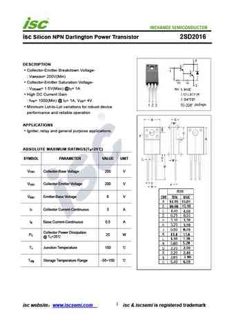
isc Silicon NPN Darlington Power Transistor 2SD2016 DESCRIPTION Collector-Emitter Breakdown Voltage- V = 200V(Min) (BR)CEO Collector-Emitter Saturation Voltage- V = 1.5V(Max) @I = 1A CE(sat) C High DC Current Gain h = 1000(Min) @ I = 1A, V = 4V FE C CE Minimum Lot-to-Lot variations for robust device performance and reliable operation APPLICATIONS Igniter, relay and
9.22. Size:210K inchange semiconductor
2sd2015.pdf 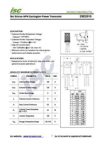
isc Silicon NPN Darlington Power Transistor 2SD2015 DESCRIPTION Collector-Emitter Breakdown Voltage- V = 120V(Min) (BR)CEO Collector-Emitter Saturation Voltage- V = 1.5V(Max) @I = 2A CE(sat) C High DC Current Gain h = 2000(Min) @ I = 2A, V = 2V FE C CE Minimum Lot-to-Lot variations for robust device performance and reliable operation APPLICATIONS Designed for drive
9.23. Size:193K inchange semiconductor
2sd201.pdf 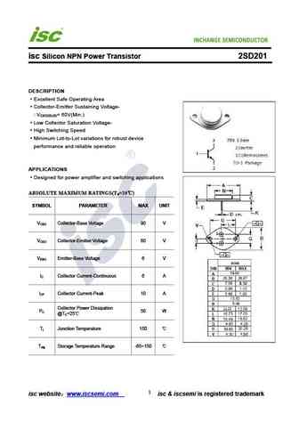
INCHANGE Semiconductor isc Silicon NPN Power Transistor 2SD201 DESCRIPTION Excellent Safe Operating Area Collector-Emitter Sustaining Voltage- V = 60V(Min.) CEO(SUS) Low Collector Saturation Voltage- High Switching Speed Minimum Lot-to-Lot variations for robust device performance and reliable operation APPLICATIONS Designed for power amplifier and switching application
9.24. Size:209K inchange semiconductor
2sd2017.pdf 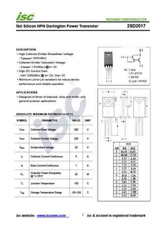
isc Silicon NPN Darlington Power Transistor 2SD2017 DESCRIPTION High Collector-Emitter Breakdown Voltage- V = 250V(Min) (BR)CEO Collector-Emitter Saturation Voltage- V = 1.5V(Max) @I = 2A CE(sat) C High DC Current Gain h = 2000(Min) @ I = 2A, V = 2V FE C CE Minimum Lot-to-Lot variations for robust device performance and reliable operation APPLICATIONS Designed of d
9.25. Size:209K inchange semiconductor
2sd2012.pdf 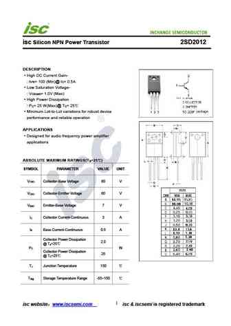
INCHANGE Semiconductor isc Silicon NPN Power Transistor 2SD2012 DESCRIPTION High DC Current Gain- h = 100 (Min)@ I = 0.5A FE C Low Saturation Voltage- V = 1.0V (Max) CE(sat) High Power Dissipation P = 25 W(Max)@ T = 25 C C Minimum Lot-to-Lot variations for robust device performance and reliable operation APPLICATIONS Designed for audio frequency power amplifier
9.26. Size:210K inchange semiconductor
2sd2014.pdf 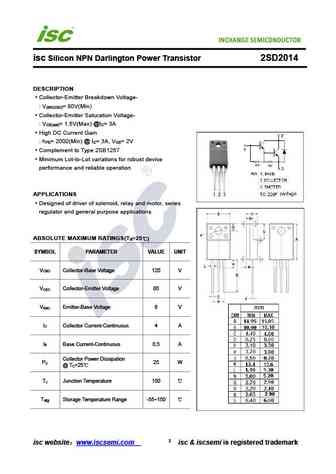
isc Silicon NPN Darlington Power Transistor 2SD2014 DESCRIPTION Collector-Emitter Breakdown Voltage- V = 80V(Min) (BR)CEO Collector-Emitter Saturation Voltage- V = 1.5V(Max) @I = 3A CE(sat) C High DC Current Gain h = 2000(Min) @ I = 3A, V = 2V FE C CE Complement to Type 2SB1257 Minimum Lot-to-Lot variations for robust device performance and reliable operation APPLI
Другие MOSFET... IRF7342PBF-1
, IRF7342QPBF
, IRF7343IPBF
, IRF7343QPBF
, IRF734PBF
, IRF7351PBF
, SD10425
, SD200DC
, IRF9540
, SD202DC
, SD203DC
, SD210
, SD2100
, SD210DE
, SD212
, SD212DE
, SD214
.