SSM3K2615R datasheet, аналоги, основные параметры
Наименование производителя: SSM3K2615R 📄📄
Тип транзистора: MOSFET
Полярность: N
Предельные значения
Pd ⓘ - Максимальная рассеиваемая мощность: 1 W
|Vds|ⓘ - Максимально допустимое напряжение сток-исток: 60 V
|Vgs|ⓘ - Максимально допустимое напряжение затвор-исток: 20 V
|Id| ⓘ - Максимально допустимый постоянный ток стока: 2 A
Tj ⓘ - Максимальная температура канала: 150 °C
Электрические характеристики
tr ⓘ - Время нарастания: 25 ns
Cossⓘ - Выходная емкость: 70 pf
RDSonⓘ - Сопротивление сток-исток открытого транзистора: 0.58 Ohm
Тип корпуса: SOT23
📄📄 Копировать
Аналог (замена) для SSM3K2615R
- подборⓘ MOSFET транзистора по параметрам
SSM3K2615R даташит
ssm3k2615r.pdf
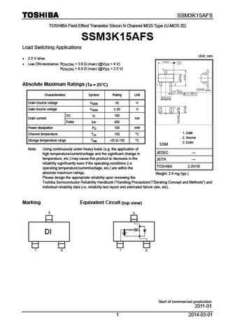
SSM3K2615R MOSFETs Silicon N-Channel MOS SSM3K2615R SSM3K2615R SSM3K2615R SSM3K2615R 1. Applications 1. Applications 1. Applications 1. Applications Load Switches Motor Drivers 2. Features 2. Features 2. Features 2. Features (1) AEC-Q101 Qualified (Note1). (2) 3.3-V gate drive voltage. (3) Low drain-source on-resistance RDS(ON) = 380 m (typ.) (@VGS = 3.3 V, ID =
ssm3k124tu .pdf
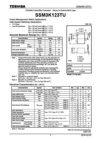
SSM3K124TU TOSHIBA Field Effect Transistor Silicon N Channel MOS Type SSM3K124TU High Speed Switching Applications Unit mm 4 V drive Low ON-resistance Ron = 120 m (max) (@VGS = 4V) 2.1 0.1 Ron = 83 m (max) (@VGS = 10V) 1.7 0.1 Absolute Maximum Ratings (Ta = 25 C) 1 Characteristic Symbol Rating Unit 3 2 Drain source voltage VDS 30 V Gate source volta
ssm3k15act.pdf
SSM3K15ACT TOSHIBA Field Effect Transistor Silicon N Channel MOS Type (U-MOS III) SSM3K15ACT Load Switching Applications Unit mm 2.5 V drive Low ON-resistance RDS(ON) = 3.6 (max) (@VGS = 4 V) RDS(ON) = 6.0 (max) (@VGS = 2.5 V) Absolute Maximum Ratings (Ta = 25 C) Characteristics Symbol Rating Unit Drain-Source voltage VDSS 30 V Gate-Source voltage VGSS 2
ssm3k104tu.pdf
SSM3K104TU TOSHIBA Field Effect Transistor Silicon N-Channel MOS Type SSM3K104TU Power Management Switch Applications High-Speed Switching Applications Unit mm Unit mm 1.8 V drive Low ON-resistance Ron = 110 m (max) (@VGS = 1.8 V) 2.1 0.1 Ron = 74 m (max) (@VGS = 2.5 V) 1.7 0.1 Ron = 56 m (max) (@VGS = 4.0 V) Absolute Maximum Ratings (Ta = 25 C) 1
ssm3k320t.pdf
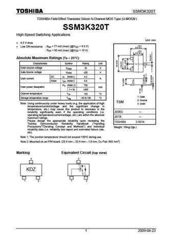
SSM3K320T TOSHIBA Field-Effect Transistor Silicon N-Channel MOS Type (U-MOS ) SSM3K320T High-Speed Switching Applications Unit mm 4.5 V drive +0.2 Low ON-resistance Ron = 77 m (max) (@VGS = 4.5 V) 2.8-0.3 Ron = 50 m (max) (@VGS = 10 V) +0.2 1.6-0.1 Absolute Maximum Ratings (Ta = 25 C) Characteristic Symbol Rating Unit Drain-Source voltage
ssm3k36fs.pdf
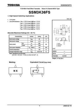
SSM3K36FS TOSHIBA Field-Effect Transistor Silicon N Channel MOS Type SSM3K36FS High-Speed Switching Applications Unit mm 1.5-V drive Low ON-resistance Ron = 1.52 (max) (@VGS = 1.5 V) Ron = 1.14 (max) (@VGS = 1.8 V) Ron = 0.85 (max) (@VGS = 2.5 V) Ron = 0.66 (max) (@VGS = 4.5 V) Ron = 0.63 (max) (@VGS = 5.0 V) Absolute Maximum Rati
ssm3k336r.pdf
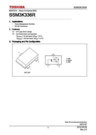
SSM3K336R MOSFETs Silicon N-Channel MOS SSM3K336R SSM3K336R SSM3K336R SSM3K336R 1. Applications 1. Applications 1. Applications 1. Applications Power Management Switches DC-DC Converters 2. Features 2. Features 2. Features 2. Features (1) 4.5 V gate drive voltage. (2) Low drain-source on-resistance RDS(ON) = 95 m (max) (@VGS = 10 V) RDS(ON) = 140 m (max) (@VG
ssm3k315t.pdf
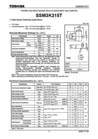
SSM3K315T TOSHIBA Field-Effect Transistor Silicon N-Channel MOS Type (U-MOS ) SSM3K315T High-Speed Switching Applications Unit mm 4.5-V drive +0.2 Low ON-resistance Ron = 41.5 m (max) (@VGS = 4.5 V) 2.8-0.3 Ron = 27.6 m (max) (@VGS = 10 V) +0.2 1.6-0.1 Absolute Maximum Ratings (Ta = 25 C) Characteristic Symbol Rating Unit Drain-Source
ssm3k116tu.pdf
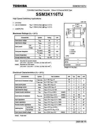
SSM3K116TU TOSHIBA Field Effect Transistor Silicon N Channel MOS Type SSM3K116TU High Speed Switching Applications Unit mm 2.5V drive 2.1 0.1 Low on-resistance Ron = 135m (max) (@VGS = 2.5 V) 1.7 0.1 Ron = 100m (max) (@VGS = 4.5 V) Lead(Pb)-free 1 Maximum Ratings (Ta = 25 C) 2 3 Characteristic Symbol Rating Unit Drain-Source voltage VDS 30 V Gate
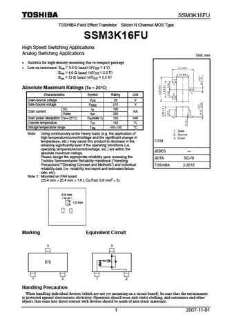
ssm3k15fu.pdf
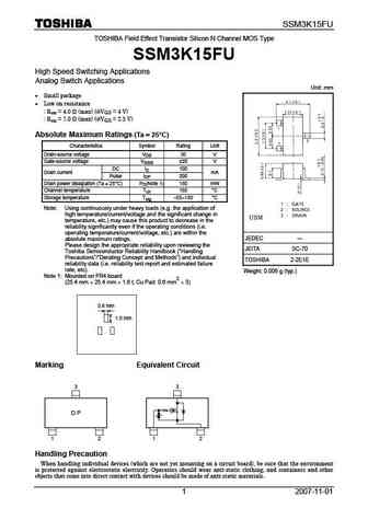
SSM3K15FU TOSHIBA Field Effect Transistor Silicon N Channel MOS Type SSM3K15FU High Speed Switching Applications Analog Switch Applications Unit mm Small package Low on resistance Ron = 4.0 (max) (@VGS = 4 V) Ron = 7.0 (max) (@VGS = 2.5 V) Absolute Maximum Ratings (Ta = 25 C) Characteristics Symbol Rating Unit Drain-source voltage VDS 30 V Gate-sour
ssm3k127tu.pdf
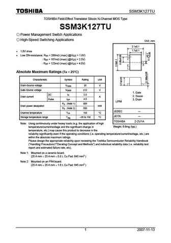
SSM3K127TU TOSHIBA Field-Effect Transistor Silicon N-Channel MOS Type SSM3K127TU Power Management Switch Applications High-Speed Switching Applications Unit mm 2.1 0.1 1.7 0.1 1.8V drive Low ON-resistance Ron = 286m (max) (@VGS = 1.8V) Ron = 167m (max) (@VGS = 2.5V) 1 Ron = 123m (max) (@VGS = 4.0V) 3 2 Absolute Maximum Ratings (Ta = 25 C
ssm3k344r.pdf
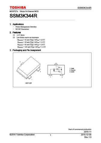
SSM3K344R MOSFETs Silicon N-Channel MOS SSM3K344R SSM3K344R SSM3K344R SSM3K344R 1. Applications 1. Applications 1. Applications 1. Applications Power Management Switches DC-DC Converters 2. Features 2. Features 2. Features 2. Features (1) 1.5 V drive (2) Low drain-source on-resistance RDS(ON) = 51 m (Typ.) (@VGS = 4.5 V) RDS(ON) = 63 m (Typ.) (@VGS = 2.5 V)
ssm3k361r.pdf
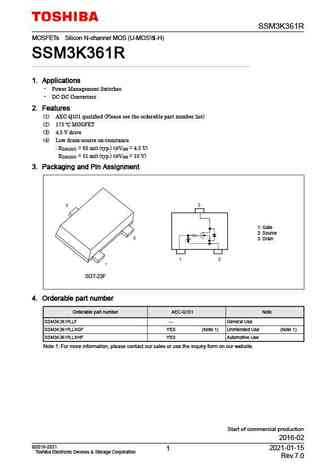
SSM3K361R MOSFETs Silicon N-channel MOS (U-MOS -H) SSM3K361R 1. Applications Power Management Switches DC-DC Converters 2. Features (1) AEC-Q101 qualified (Please see the orderable part number list) (2) 175 MOSFET (3) 4.5 V drive (4) Low drain-source on-resistance RDS(ON) = 65 m (typ.) (@VGS = 4.5 V) RDS(ON) = 51 m (typ.) (@VGS = 10 V) 3. Packaging and Pin As
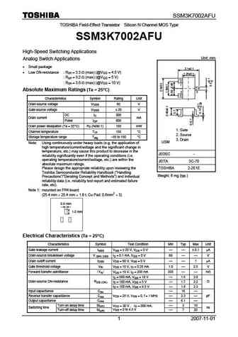
ssm3k7002fu.pdf
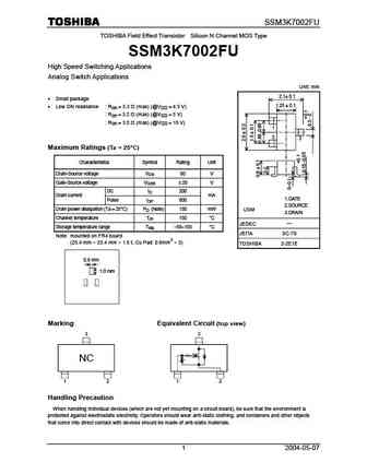
SSM3K7002FU TOSHIBA Field Effect Transistor Silicon N Channel MOS Type SSM3K7002FU High Speed Switching Applications Analog Switch Applications Unit mm 2.1 0.1 Small package 1.25 0.1 Low ON resistance Ron = 3.3 (max) (@VGS = 4.5 V) Ron = 3.2 (max) (@VGS = 5 V) Ron = 3.0 (max) (@VGS = 10 V) 1 2 3 Maximum Ratings (Ta = 25 C) Characteris
ssm3k302t.pdf
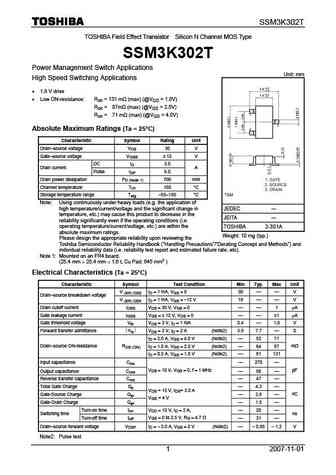
SSM3K302T TOSHIBA Field Effect Transistor Silicon N Channel MOS Type SSM3K302T Power Management Switch Applications Unit mm High Speed Switching Applications 1.8 V drive Low ON-resistance Ron = 131 m (max) (@VGS = 1.8V) Ron = 87m (max) (@VGS = 2.5V) Ron = 71 m (max) (@VGS = 4.0V) Absolute Maximum Ratings (Ta = 25 C) Characteristic Symbol Rating Unit Dr
ssm3k7002afu.pdf
SSM3K7002AFU TOSHIBA Field-Effect Transistor Silicon N Channel MOS Type SSM3K7002AFU High-Speed Switching Applications Unit mm Analog Switch Applications Small package 2.1 0.1 Low ON-resistance Ron = 3.3 (max) (@VGS = 4.5 V) 1.25 0.1 Ron = 3.2 (max) (@VGS = 5 V) Ron = 3.0 (max) (@VGS = 10 V) 1 Absolute Maximum Ratings (Ta = 25 C) 23 Characteri
ssm3k01f.pdf
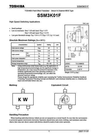
SSM3K01F TOSHIBA Field Effect Transistor Silicon N Channel MOS Type SSM3K01F High Speed Switching Applications Unit mm Small package Low on resistance Ron = 120 m (max) (VGS = 4 V) Ron = 150 m (max) (VGS = 2.5 V) Low gate threshold voltage Vth = 0.6 1.1 V (VDS = 3 V, ID = 0.1 mA) Absolute Maximum Ratings (Ta = 25 C) Characteristics Symbol Rating Uni
ssm3k15f.pdf
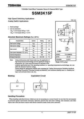
SSM3K15F TOSHIBA Field Effect Transistor Silicon N Channel MOS Type SSM3K15F High Speed Switching Applications Unit mm Analog Switch Applications +0.5 2.5-0.3 +0.25 Small package 1.5-0.15 Low on resistance Ron = 4.0 (max) (@VGS = 4 V) 1 Ron = 7.0 (max) (@VGS = 2.5 V) 2 3 Absolute Maximum Ratings (Ta = 25 C) Characteristics Symbol Rating Unit Drai
ssm3k7002af.pdf
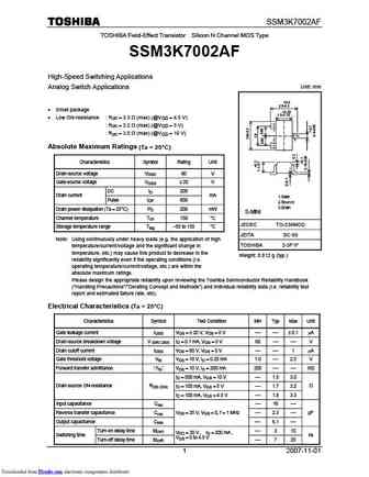
SSM3K7002AF TOSHIBA Field-Effect Transistor Silicon N Channel MOS Type SSM3K7002AF High-Speed Switching Applications Unit mm Analog Switch Applications +0.5 2.5-0.3 Small package +0.25 1.5-0.15 Low ON-resistance Ron = 3.3 (max) (@VGS = 4.5 V) Ron = 3.2 (max) (@VGS = 5 V) 1 Ron = 3.0 (max) (@VGS = 10 V) 2 3 Absolute Maximum Ratings (Ta = 25 C)
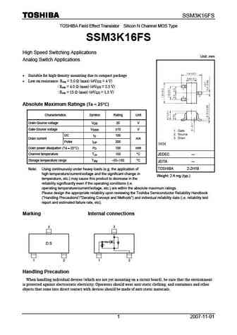
ssm3k15fs .pdf
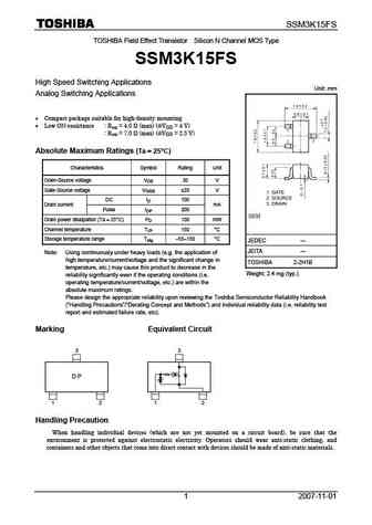
SSM3K15FS TOSHIBA Field Effect Transistor Silicon N Channel MOS Type SSM3K15FS High Speed Switching Applications Unit mm Analog Switching Applications Compact package suitable for high-density mounting Low ON-resistance Ron = 4.0 (max) (@VGS = 4 V) Ron = 7.0 (max) (@VGS = 2.5 V) Absolute Maximum Ratings (Ta = 25 C) Characteristics Symbol Rating Unit Dr
ssm3k37ct.pdf
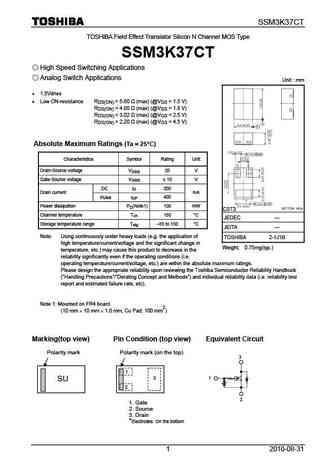
SSM3K37CT TOSHIBA Field Effect Transistor Silicon N Channel MOS Type SSM3K37CT High Speed Switching Applications Analog Switch Applications Unit mm 1.5Vdrive Low ON-resistance RDS(ON) = 5.60 (max) (@VGS = 1.5 V) RDS(ON) = 4.05 (max) (@VGS = 1.8 V) RDS(ON) = 3.02 (max) (@VGS = 2.5 V) RDS(ON) = 2.20 (max) (@VGS = 4.5 V) Absolute Maximum Ratin
ssm3k44mfv.pdf
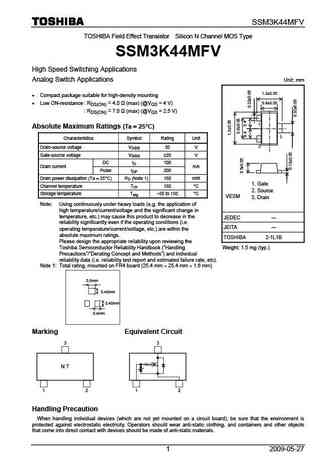
SSM3K44MFV TOSHIBA Field Effect Transistor Silicon N Channel MOS Type SSM3K44MFV High Speed Switching Applications Analog Switch Applications Unit mm 1.2 0.05 Compact package suitable for high-density mounting 0.8 0.05 Low ON-resistance RDS(ON) = 4.0 (max) (@VGS = 4 V) RDS(ON) = 7.0 (max) (@VGS = 2.5 V) 1 Absolute Maximum Ratings (Ta = 25 C) 3 Chara
ssm3k05fu.pdf
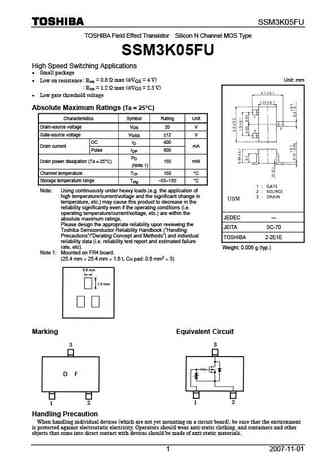
SSM3K05FU TOSHIBA Field Effect Transistor Silicon N Channel MOS Type SSM3K05FU High Speed Switching Applications Small package Unit mm Low on resistance Ron = 0.8 max (@VGS = 4 V) Ron = 1.2 max (@VGS = 2.5 V) Low gate threshold voltage Absolute Maximum Ratings (Ta = 25 C) Characteristics Symbol Rating Unit Drain-source voltage VDS 20 V Gate-source
ssm3k09fu.pdf
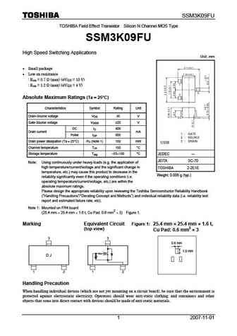
SSM3K09FU TOSHIBA Field Effect Transistor Silicon N Channel MOS Type SSM3K09FU High Speed Switching Applications Unit mm Small package Low on resistance Ron = 0.7 (max) (@VGS = 10 V) Ron = 1.2 (max) (@VGS = 4 V) Absolute Maximum Ratings (Ta = 25 C) Characteristics Symbol Rating Unit Drain-Source voltage VDS 30 V Gate-Source voltage VGSS 20 V DC ID
ssm3k36mfv.pdf
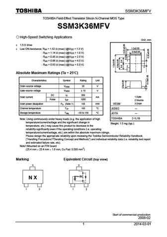
SSM3K36MFV TOSHIBA Field-Effect Transistor Silicon N-Channel MOS Type SSM3K36MFV High-Speed Switching Applications Unit mm 1.5-V drive 1.2 0.05 Low ON-resistance Ron = 1.52 (max) (@VGS = 1.5 V) 0.8 0.05 Ron = 1.14 (max) (@VGS = 1.8 V) Ron = 0.85 (max) (@VGS = 2.5 V) Ron = 0.66 (max) (@VGS = 4.5 V) 1 Ron = 0.63 (max) (@VGS = 5.0 V)
ssm3k17fu.pdf
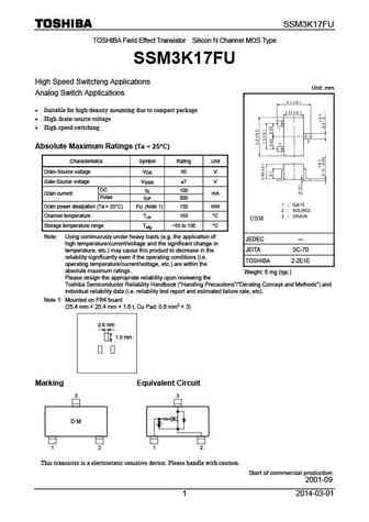
SSM3K17FU TOSHIBA Field Effect Transistor Silicon N Channel MOS Type SSM3K17FU High Speed Switching Applications Unit mm Analog Switch Applications Suitable for high-density mounting due to compact package High drain-source voltage High speed switching Absolute Maximum Ratings (Ta = 25 C) Characteristics Symbol Rating Unit Drain-Source voltage VDS 50 V Gate-S
ssm3k35ctc.pdf
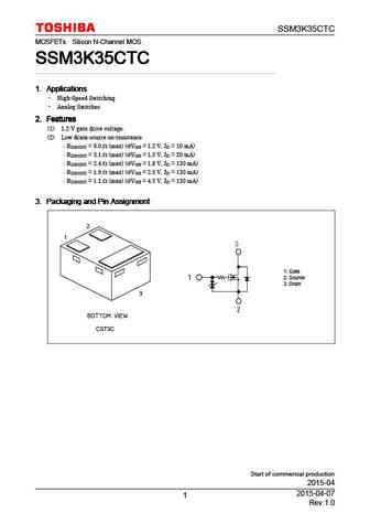
SSM3K35CTC MOSFETs Silicon N-Channel MOS SSM3K35CTC SSM3K35CTC SSM3K35CTC SSM3K35CTC 1. Applications 1. Applications 1. Applications 1. Applications High-Speed Switching Analog Switches 2. Features 2. Features 2. Features 2. Features (1) 1.2-V gate drive voltage. (2) Low drain-source on-resistance RDS(ON) = 9.0 (max) (@VGS = 1.2 V, ID = 10 mA) RDS(ON) = 3.1
ssm3k310t.pdf
SSM3K310T TOSHIBA Field Effect Transistor Silicon N-Channel MOS Type SSM3K310T High-Speed Switching Applications 1.5 V drive Unit mm Low ON-resistance Ron = 66 m (max) (@VGS = 1.5 V) +0.2 2.8-0.3 Ron = 43 m (max) (@VGS = 1.8 V) +0.2 Ron = 32 m (max) (@VGS = 2.5 V) 1.6-0.1 Ron = 28 m (max) (@VGS = 4.0 V) Absolute Maximum Ratings (Ta = 25 C)
ssm3k124tu.pdf
SSM3K124TU TOSHIBA Field Effect Transistor Silicon N Channel MOS Type SSM3K124TU High Speed Switching Applications Unit mm 4 V drive 2.1 0.1 Low ON-resistance Ron = 120 m (max) (@VGS = 4V) 1.7 0.1 Ron = 83 m (max) (@VGS = 10V) Lead(Pb)-free 1 2 3 Maximum Ratings (Ta = 25 C) Characteristic Symbol Rating Unit Drain source voltage VDS 30 V Gate so
ssm3k107tu.pdf
SSM3K107TU TOSHIBA Field Effect Transistor Silicon N Channel MOS Type SSM3K107TU High-Speed Switching Applications Unit mm 4 V drive 2.1 0.1 Low ON-resistance Ron = 410 m (max) (@VGS = 4V) 1.7 0.1 Ron = 200 m (max) (@VGS = 10V) Lead(Pb)-free 1 2 3 Maximum Ratings (Ta = 25 C) Characteristic Symbol Rating Unit Drain source voltage VDS 20 V Gate s
ssm3k16te.pdf
SSM3K16TE TOSHIBA Field Effect Transistor Silicon N Channel MOS Type SSM3K16TE High Speed Switching Applications Unit mm Analog Switch Applications Suitable for high-density mounting due to compact package Low on resistance Ron = 3.0 (max) (@VGS = 4 V) Ron = 4.0 (max) (@VGS = 2.5 V) Ron = 15 (max) (@VGS = 1.5 V) Absolute Maximum Ratings (Ta = 25 C)
ssm3k59ctb.pdf
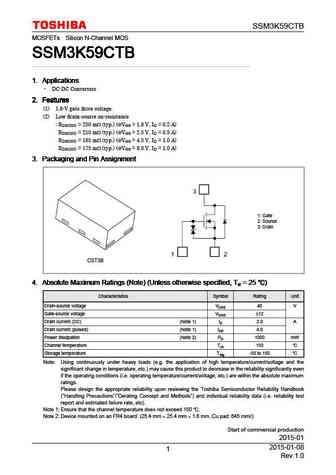
SSM3K59CTB MOSFETs Silicon N-Channel MOS SSM3K59CTB SSM3K59CTB SSM3K59CTB SSM3K59CTB 1. Applications 1. Applications 1. Applications 1. Applications DC-DC Converters 2. Features 2. Features 2. Features 2. Features (1) 1.8-V gate drive voltage. (2) Low drain-source on-resistance RDS(ON) = 250 m (typ.) (@VGS = 1.8 V, ID = 0.2 A) RDS(ON) = 210 m (typ.) (@VGS = 2.5 V,
ssm3k128tu.pdf
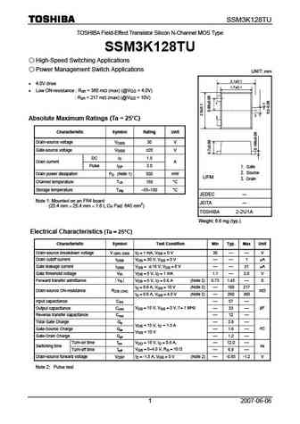
SSM3K128TU TOSHIBA Field-Effect Transistor Silicon N-Channel MOS Type SSM3K128TU High-Speed Switching Applications Power Management Switch Applications UNIT mm 2.1 0.1 4.0V drive 1.7 0.1 Low ON-resistance Ron = 360 m (max) (@VGS = 4.0V) Ron = 217 m (max) (@VGS = 10V) 1 3 2 Absolute Maximum Ratings (Ta = 25 C) Characteristic Symbol Rating Uni
ssm3k15fv.pdf
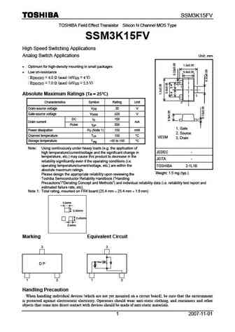
SSM3K15FV TOSHIBA Field Effect Transistor Silicon N Channel MOS Type SSM3K15FV High Speed Switching Applications Analog Switch Applications Unit mm 1.2 0.05 Optimum for high-density mounting in small packages 0.8 0.05 Low on-resistance RDS(ON) = 4.0 (max) (@VGS = 4 V) RDS(ON) = 7.0 (max) (@VGS = 2.5 V) 1 Absolute Maximum Ratings (Ta = 25 C) 3 Char
ssm3k56mfv.pdf
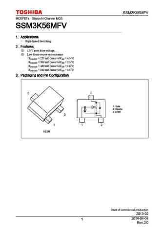
SSM3K56MFV MOSFETs Silicon N-Channel MOS SSM3K56MFV SSM3K56MFV SSM3K56MFV SSM3K56MFV 1. Applications 1. Applications 1. Applications 1. Applications High-Speed Switching 2. Features 2. Features 2. Features 2. Features (1) 1.5-V gate drive voltage. (2) Low drain-source on-resistance RDS(ON) = 235 m (max) (@VGS = 4.5 V) RDS(ON) = 300 m (max) (@VGS = 2.5 V) RDS(ON)
ssm3k37mfv.pdf
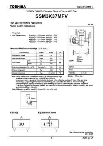
SSM3K37MFV TOSHIBA Field-Effect Transistor Silicon N-Channel MOS Type SSM3K37MFV High Speed Switching Applications nit mm Analog Switch Applications 1.2 0.05 0.8 0.05 1.5-V drive Low ON-resistance RDS(ON) = 5.60 (max) (@VGS = 1.5 V) RDS(ON) = 4.05 (max) (@VGS = 1.8 V) 1 RDS(ON) = 3.02 (max) (@VGS = 2.5 V) RDS(ON) = 2.20 (max) (@VGS = 4.5 V) 2
ssm3k35amfv.pdf
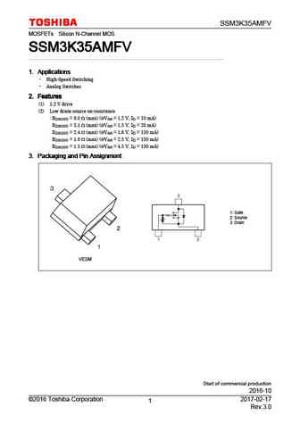
SSM3K35AMFV MOSFETs Silicon N-Channel MOS SSM3K35AMFV SSM3K35AMFV SSM3K35AMFV SSM3K35AMFV 1. Applications 1. Applications 1. Applications 1. Applications High-Speed Switching Analog Switches 2. Features 2. Features 2. Features 2. Features (1) 1.2 V drive (2) Low drain-source on-resistance RDS(ON) = 9.0 (max) (@VGS = 1.2 V, ID = 10 mA) RDS(ON) = 3.1 (max) (@
ssm3k7002cfu.pdf
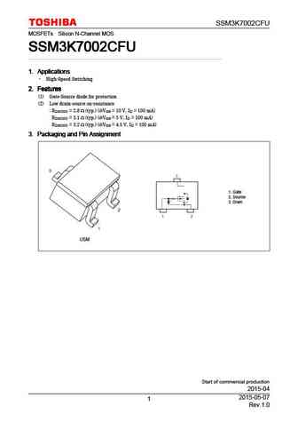
SSM3K7002CFU MOSFETs Silicon N-Channel MOS SSM3K7002CFU SSM3K7002CFU SSM3K7002CFU SSM3K7002CFU 1. Applications 1. Applications 1. Applications 1. Applications High-Speed Switching 2. Features 2. Features 2. Features 2. Features (1) Gate-Source diode for protection (2) Low drain-source on-resistance RDS(ON) = 2.8 (typ.) (@VGS = 10 V, ID = 100 mA) RDS(ON) = 3.1 (t
ssm3k123tu.pdf
SSM3K123TU TOSHIBA Field Effect Transistor Silicon N-Channel MOS Type SSM3K123TU Power Management Switch Applications High-Speed Switching Applications Unit mm Unit mm 1.5 V drive Low ON-resistance Ron = 66 m (max) (@VGS = 1.5 V) Ron = 43 m (max) (@VGS = 1.8 V) 2.1 0.1 Ron = 32 m (max) (@VGS = 2.5 V) 1.7 0.1 Ron = 28 m (max) (@VGS = 4.0 V) Absol
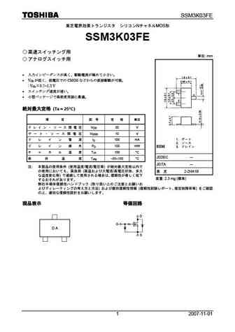
ssm3k03te.pdf
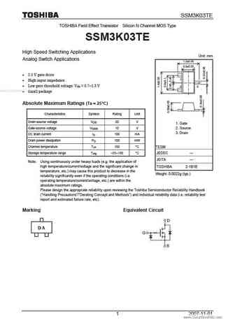
SSM3K03TE TOSHIBA Field Effect Transistor Silicon N Channel MOS Type SSM3K03TE High Speed Switching Applications Unit mm Analog Switch Applications 1.2 0.05 0.8 0.05 2.5 V gate drive High input impedance Low gate threshold voltage Vth = 0.7 1.3 V www.DataSheet4U.com Small package Absolute Maximum Ratings (Ta = 25 C) Characteristics Symb
ssm3k56fs.pdf
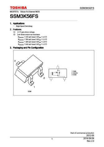
SSM3K56FS MOSFETs Silicon N-Channel MOS SSM3K56FS SSM3K56FS SSM3K56FS SSM3K56FS 1. Applications 1. Applications 1. Applications 1. Applications High-Speed Switching 2. Features 2. Features 2. Features 2. Features (1) 1.5-V gate drive voltage. (2) Low drain-source on-resistance RDS(ON) = 235 m (max) (@VGS = 4.5 V) RDS(ON) = 300 m (max) (@VGS = 2.5 V) RDS(ON) = 48
ssm3k15ct.pdf
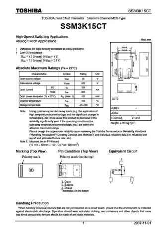
SSM3K15CT TOSHIBA Field Effect Transistor Silicon N-Channel MOS Type SSM3K15CT High-Speed Switching Applications Unit mm Analog Switch Applications 0.6 0.05 Optimum for high-density mounting in small packages 0.5 0.03 Low ON-resistance Ron = 4.0 (max) (@VGS = 4 V) Ron = 7.0 (max) (@VGS = 2.5 V) Absolute Maximum Ratings (Ta = 25 C) Ch
ssm3k119tu.pdf
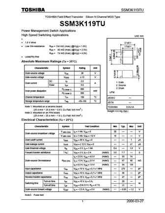
SSM3K119TU TOSHIBA Field Effect Transistor Silicon N Channel MOS Type SSM3K119TU Power Management Switch Applications High Speed Switching Applications Unit mm 1.8 V drive 2.1 0.1 Low ON-resistance Ron = 134 m (max) (@VGS = 1.8V) 1.7 0.1 Ron = 90 m (max) (@VGS = 2.5V) Ron = 74 m (max) (@VGS = 4.0V) 1 Lead(Pb)-free 2 3 Absolute Maximum Ra
ssm3k7002bfu.pdf
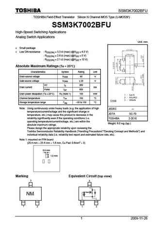
SSM3K7002BFU TOSHIBA Field-Effect Transistor Silicon N Channel MOS Type (U-MOS ) SSM3K7002BFU High-Speed Switching Applications Analog Switch Applications Unit mm Small package Low ON-resistance RDS(ON) = 3.3 (max) (@VGS = 4.5 V) RDS(ON) = 2.6 (max) (@VGS = 5 V) RDS(ON) = 2.1 (max) (@VGS = 10 V) Absolute Maximum Ratings (Ta = 25 C) Characteristics
ssm3k101tu.pdf

SSM3K101TU TOSHIBA Field Effect Transistor Silicon N Channel MOS Type SSM3K101TU High Speed Switching Applications Unit mm 1.8V drive 2.1 0.1 Low on-resistance Ron = 230m (max) (@VGS = 1.8 V) 1.7 0.1 Ron = 138m (max) (@VGS = 2.5 V) Ron = 103m (max) (@VGS = 4.0 V) Lead(Pb)-free 1 2 3 Maximum Ratings (Ta = 25 C) Characteristic Symbol Rating Unit
ssm3k7002bf.pdf
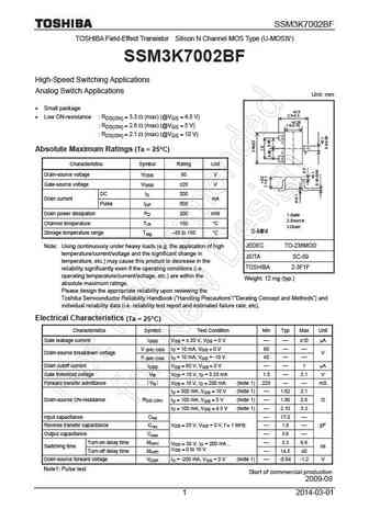
SSM3K7002BF TOSHIBA Field-Effect Transistor Silicon N Channel MOS Type (U-MOS ) SSM3K7002BF High-Speed Switching Applications Analog Switch Applications Unit mm Small package +0.5 2.5-0.3 Low ON-resistance RDS(ON) = 3.3 (max) (@VGS = 4.5 V) +0.25 1.5-0.15 RDS(ON) = 2.6 (max) (@VGS = 5 V) RDS(ON) = 2.1 (max) (@VGS = 10 V) 1 Absolute Maximum Rating
ssm3k04fe.pdf
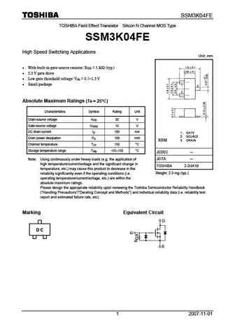
SSM3K04FE TOSHIBA Field Effect Transistor Silicon N Channel MOS Type SSM3K04FE High Speed Switching Applications Unit mm With built-in gate-source resistor RGS = 1 M (typ.) 2.5 V gate drive Low gate threshold voltage Vth = 0.7 1.3 V Small package Absolute Maximum Ratings (Ta = 25 C) Characteristics Symbol Rating Unit Drain-source voltage VDS 20 V Gat
ssm3k16fs.pdf
SSM3K16FS TOSHIBA Field Effect Transistor Silicon N Channel MOS Type SSM3K16FS High Speed Switching Applications Unit mm Analog Switch Applications Suitable for high-density mounting due to compact package Low on resistance Ron = 3.0 (max) (@VGS = 4 V) Ron = 4.0 (max) (@VGS = 2.5 V) Ron = 15 (max) (@VGS = 1.5 V) Absolute Maximum Ratings (Ta = 25 C)
ssm3k37fs.pdf
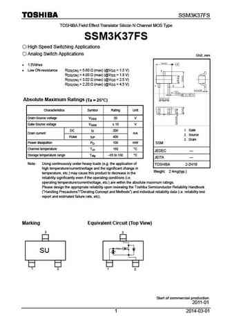
SSM3K37FS TOSHIBA Field Effect Transistor Silicon N Channel MOS Type SSM3K37FS High Speed Switching Applications Analog Switch Applications Unit mm 1.5Vdrive Low ON-resistance RDS(ON) = 5.60 (max) (@VGS = 1.5 V) RDS(ON) = 4.05 (max) (@VGS = 1.8 V) RDS(ON) = 3.02 (max) (@VGS = 2.5 V) RDS(ON) = 2.20 (max) (@VGS = 4.5 V) Absolute Maximum Rating
ssm3k15amfv.pdf
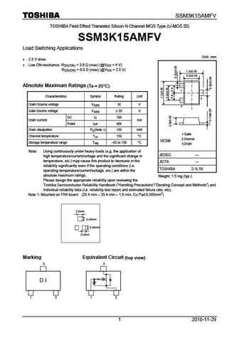
SSM3K15AMFV TOSHIBA Field Effect Transistor Silicon N Channel MOS Type (U-MOS III) SSM3K15AMFV Load Switching Applications Unit mm 2.5 V drive Low ON-resistance RDS(ON) = 3.6 (max) (@VGS = 4 V) RDS(ON) = 6.0 (max) (@VGS = 2.5 V) 1.2 0.05 0.8 0.05 Absolute Maximum Ratings (Ta = 25 C) 1 Characteristics Symbol Rating Unit 3 Drain-Source voltage VDSS 30 V
ssm3k72ctc.pdf
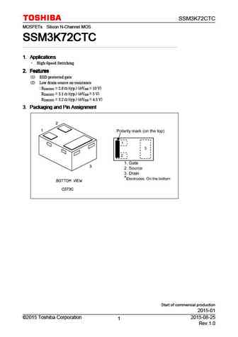
SSM3K72CTC MOSFETs Silicon N-Channel MOS SSM3K72CTC SSM3K72CTC SSM3K72CTC SSM3K72CTC 1. Applications 1. Applications 1. Applications 1. Applications High-Speed Switching 2. Features 2. Features 2. Features 2. Features (1) ESD protected gate (2) Low drain-source on-resistance RDS(ON) = 2.8 (typ.) (@VGS = 10 V) RDS(ON) = 3.1 (typ.) (@VGS = 5 V) RDS(ON) = 3.2
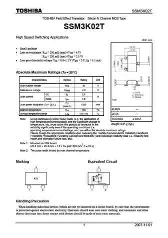
ssm3k12t.pdf
SSM3K12T TOSHIBA Field Effect Transistor Silicon N Channel MOS Type SSM3K12T DC-DC Converter Unit mm High Speed Switching Applications Small Package Low ON-resistance Ron = 95 m (max) (@VGS = 10 V) Ron = 145 m (max) (@VGS = 4.5 V) High speed ton = 21 ns toff = 16 ns Absolute Maximum Ratings (Ta = 25 C) Characteristics Symbol Rating Unit Drain
ssm3k122tu.pdf
SSM3K122TU TOSHIBA Field Effect Transistor Silicon N-Channel MOS Type SSM3K122TU Power Management Switch Applications High-Speed Switching Applications 1.5 V drive Unit mm Unit mm Low ON-resistance Ron = 304 m (max) (@VGS = 1.5 V) 2.1 0.1 Ron = 211 m (max) (@VGS = 1.8 V) 1.7 0.1 Ron = 161 m (max) (@VGS = 2.5 V) Ron = 123 m (max) (@VGS = 4.0 V) 1
ssm3k318t.pdf
SSM3K318T TOSHIBA Field-Effect Transistor Silicon N-Channel MOS Type (U-MOS ) SSM3K318T Load Switching Applications High-Speed Switching Applications Unit mm +0.2 4.5 V drive 2.8-0.3 Low ON-resistance RDS(ON) = 145 m (max) (@VGS = 4.5 V) +0.2 1.6-0.1 RDS(ON) = 107 m (max) (@VGS = 10 V) Absolute Maximum Ratings (Ta = 25 C) Characteristic Sy
ssm3k56act.pdf
SSM3K56ACT MOSFETs Silicon N-Channel MOS SSM3K56ACT SSM3K56ACT SSM3K56ACT SSM3K56ACT 1. Applications 1. Applications 1. Applications 1. Applications High-Speed Switching 2. Features 2. Features 2. Features 2. Features (1) 1.5-V gate drive voltage. (2) Low drain-source on-resistance RDS(ON) = 235 m (max) (@VGS = 4.5 V) RDS(ON) = 300 m (max) (@VGS = 2.5 V) RDS(ON)
ssm3k318r.pdf
SSM3K318R MOSFETs Silicon N-Channel MOS SSM3K318R SSM3K318R SSM3K318R SSM3K318R 1. Applications 1. Applications 1. Applications 1. Applications Load Switches Ultra-High-Speed Switching 2. Features 2. Features 2. Features 2. Features (1) 4.5-V gate drive voltage. (2) Low drain-source on-resistance RDS(ON) = 145 m (max) (@VGS = 4.5 V) RDS(ON) = 107 m (max) (@VGS
ssm3k04fv.pdf
SSM3K04FV TOSHIBA Field Effect Transistor Silicon N Channel MOS Type SSM3K04FV High Speed Switching Applications Unit mm 1.2 0.05 With built-in gate-source resistor RGS = 1 M (typ.) 0.8 0.05 2.5 V gate drive High input impedance Low gate threshold voltage Vth = 0.7 1.3 V 1 Optimum for high-density mounting in small packages www.DataSheet4U.com
ssm3k7002bfs.pdf
SSM3K7002BFS TOSHIBA Field-Effect Transistor Silicon N Channel MOS Type (U-MOS ) SSM3K7002BFS High-Speed Switching Applications Analog Switch Applications Unit mm Small package Low ON-resistance RDS(ON) = 3.3 (max) (@VGS = 4.5 V) RDS(ON) = 2.6 (max) (@VGS = 5 V) RDS(ON) = 2.1 (max) (@VGS = 10 V) Absolute Maximum Ratings (Ta = 25 C) Characteristics
ssm3k102tu.pdf
SSM3K102TU TOSHIBA Field Effect Transistor Silicon N Channel MOS Type SSM3K102TU High Speed Switching Applications Unit mm 1.8V drive 2.1 0.1 Low on-resistance Ron = 154m (max) (@VGS = 1.8 V) 1.7 0.1 Ron = 99m (max) (@VGS = 2.5 V) Ron = 71m (max) (@VGS = 4.0 V) Lead(Pb)-free 1 2 3 Maximum Ratings (Ta = 25 C) Characteristic Symbol Rating Unit
ssm3k309t.pdf
SSM3K309T TOSHIBA Field-Effect Transistor Silicon N-Channel MOS Type SSM3K309T Power Management Switch Applications High-Current Switching Applications Unit mm 1.8V drive Low on-resistance Ron = 47m (max) (@VGS = 1.8V) Ron = 35m (max) (@VGS = 2.5V) Ron = 31m (max) (@VGS = 4.0V) Absolute Maximum Ratings (Ta = 25 C) Characteristic Symbol Rating
ssm3k01t.pdf
SSM3K01T TOSHIBA Field Effect Transistor Silicon N Channel MOS Type SSM3K01T High Speed Switching Applications Unit mm Small Package Low on Resistance Ron = 120 m (max) (@VGS = 4 V) Ron = 150 m (max) (@VGS = 2.5 V) Low Gate Threshold Voltage Vth = 0.6 1.1 V (@VDS = 3 V, ID = 0.1 mA) Absolute Maximum Ratings (Ta = 25 C) Characteristics Symbol Rating
ssm3k02f.pdf
SSM3K02F TOSHIBA Field Effect Transistor Silicon N Channel MOS Type SSM3K02F High Speed Switching Applications Unit mm Small package Low on resistance Ron = 200 m (max) (VGS = 4 V) Ron = 250 m (max) (VGS = 2.5 V) Low gate threshold voltage Vth = 0.6 1.1 V (VDS = 3 V, ID = 0.1 mA) Absolute Maximum Ratings (Ta = 25 C) Characteristics Symbol Rating Unit
ssm3k15fs.pdf
SSM3K15FS TOSHIBA Field Effect Transistor Silicon N Channel MOS Type SSM3K15FS High Speed Switching Applications Unit mm Analog Switching Applications Compact package suitable for high-density mounting Low ON-resistance R = 4.0 (max) (@V = 4 V) on GS R = 7.0 (max) (@V = 2.5 V) on GS Maximum Ratings (Ta = = 25 C) = = Characteristic Symbol Rating Uni
ssm3k121tu.pdf
SSM3K121TU TOSHIBA Field Effect Transistor Silicon N-Channel MOS Type SSM3K121TU Power Management Switch Applications High-Speed Switching Applications Unit mm Unit mm 1.5 V drive Low ON-resistance Ron = 140 m (max) (@VGS = 1.5 V) Ron = 93 m (max) (@VGS = 1.8 V) 2.1 0.1 Ron = 63 m (max) (@VGS = 2.5 V) 1.7 0.1 Ron = 48 m (max) (@VGS = 4.0 V) Absolu
ssm3k16fv.pdf
SSM3K16FV TOSHIBA Field Effect Transistor Silicon N Channel MOS Type SSM3K16FV High Speed Switching Applications nit mm Analog Switch Applications 1.2 0.05 Suitable for high-density mounting due to compact package 0.8 0.05 Low on-resistance Ron = 3.0 (max) (@VGS = 4 V) Ron = 4.0 (max) (@VGS = 2.5 V) Ron = 15 (max) (@VGS = 1.5 V) 1 Absolute Max
ssm3k126tu.pdf
SSM3K126TU TOSHIBA Field Effect Transistor Silicon N-Channel MOS Type SSM3K126TU High-Speed Switching Applications 4.0 V drive Unit mm Low ON-resistance Ron = 43 m (max) (@VGS = 4.0 V) Ron = 32 m (max) (@VGS = 10 V) 2.1 0.1 1.7 0.1 Absolute Maximum Ratings (Ta = 25 C) Characteristics Symbol Rating Unit 1 Drain-Source voltage VDSS 30 V Gate-Source voltag
ssm3k301t.pdf
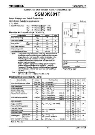
SSM3K301T TOSHIBA Field Effect Transistor Silicon N-Channel MOS Type SSM3K301T Power Management Switch Applications Unit mm High-Speed Switching Applications Unit mm 1.8 V drive Low ON-resistance Ron = 110 m (max) (@VGS = 1.8 V) Ron = 74 m (max) (@VGS = 2.5 V) Ron = 56 m (max) (@VGS = 4.0 V) Absolute Maximum Ratings (Ta = 25 C) Characteristics Symbol
ssm3k14t.pdf
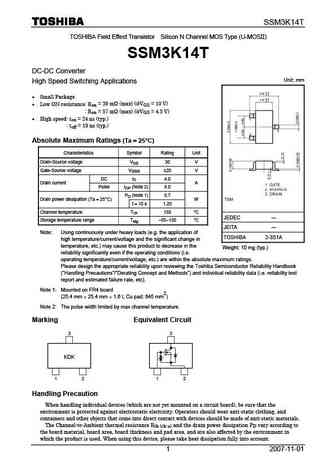
SSM3K14T TOSHIBA Field Effect Transistor Silicon N Channel MOS Type (U-MOSII) SSM3K14T DC-DC Converter Unit mm High Speed Switching Applications Small Package Low ON-resistance Ron = 39 m (max) (@VGS = 10 V) Ron = 57 m (max) (@VGS = 4.5 V) High speed ton = 24 ns (typ.) toff = 19 ns (typ.) Absolute Maximum Ratings (Ta = 25 C) Characteristics Symbo
ssm3k339r.pdf

SSM3K339R MOSFETs Silicon N-Channel MOS SSM3K339R SSM3K339R SSM3K339R SSM3K339R 1. Applications 1. Applications 1. Applications 1. Applications Power Management Switches DC-DC Converters 2. Features 2. Features 2. Features 2. Features (1) 1.8-V gate drive voltage. (2) Low drain-source on-resistance RDS(ON) = 145 m (typ.) (@VGS = 8.0 V, ID = 1.0 A) RDS(ON) = 155
ssm3k311t.pdf
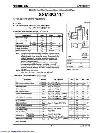
SSM3K311T TOSHIBA Field-Effect Transistor Silicon N-Channel MOS Type SSM3K311T High-Speed Switching Applications Unit mm 4 V drive Low ON-resistance Ron = 43m (max) (@VGS = 4V) +0.2 2.8-0.3 Ron = 32m (max) (@VGS = 10V) +0.2 1.6-0.1 Absolute Maximum Ratings (Ta = 25 C) Characteristic Symbol Rating Unit Drain source voltage VDS 30 V Gat
ssm3k15afs.pdf
SSM3K15AFS TOSHIBA Field Effect Transistor Silicon N Channel MOS Type (U-MOS III) SSM3K15AFS Load Switching Applications Unit mm 2.5 V drive Low ON-resistance RDS(ON) = 3.6 (max) (@VGS = 4 V) RDS(ON) = 6.0 (max) (@VGS = 2.5 V) Absolute Maximum Ratings (Ta = 25 C) Characteristics Symbol Rating Unit Drain-Source voltage VDSS 30 V Gate-Source voltage VGSS 2
ssm3k56ct.pdf
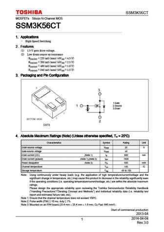
SSM3K56CT MOSFETs Silicon N-Channel MOS SSM3K56CT SSM3K56CT SSM3K56CT SSM3K56CT 1. Applications 1. Applications 1. Applications 1. Applications High-Speed Switching 2. Features 2. Features 2. Features 2. Features (1) 1.5-V gate drive voltage. (2) Low drain-source on-resistance RDS(ON) = 235 m (max) (@VGS = 4.5 V) RDS(ON) = 300 m (max) (@VGS = 2.5 V) RDS(ON) = 48
ssm3k02t.pdf
SSM3K02T TOSHIBA Field Effect Transistor Silicon N Channel MOS Type SSM3K02T High Speed Switching Applications Unit mm Small package Low on resistance Ron = 200 m (max) (VGS = 4 V) Ron = 250 m (max) (VGS = 2.5 V) Low gate threshold voltage Vth = 0.6 1.1 V (VDS = 3 V, ID = 0.1 mA) Absolute Maximum Ratings (Ta = 25 C) Characteristics Symbol Rating Unit
ssm3k329r.pdf
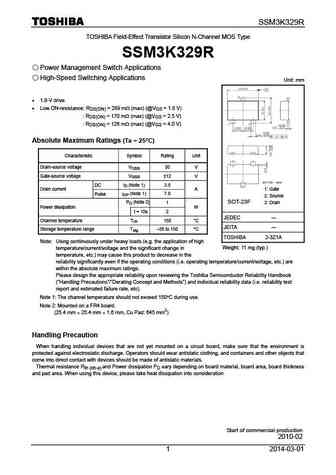
SSM3K329R TOSHIBA Field-Effect Transistor Silicon N-Channel MOS Type SSM3K329R Power Management Switch Applications High-Speed Switching Applications Unit mm 1.8-V drive Low ON-resistance RDS(ON) = 289 m (max) (@VGS = 1.8 V) RDS(ON) = 170 m (max) (@VGS = 2.5 V) RDS(ON) = 126 m (max) (@VGS = 4.0 V) Absolute Maximum Ratings (Ta = 25 C) Characte
ssm3k105tu.pdf
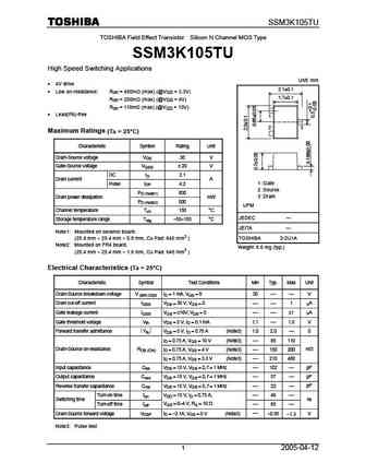
SSM3K105TU TOSHIBA Field Effect Transistor Silicon N Channel MOS Type SSM3K105TU High Speed Switching Applications Unit mm 4V drive 2.1 0.1 Low on-resistance Ron = 480m (max) (@VGS = 3.3V) 1.7 0.1 Ron = 200m (max) (@VGS = 4V) Ron = 110m (max) (@VGS = 10V) Lead(Pb)-free 1 2 3 Maximum Ratings (Ta = 25 C) Characteristic Symbol Rating Unit Drain-
ssm3k35fs.pdf
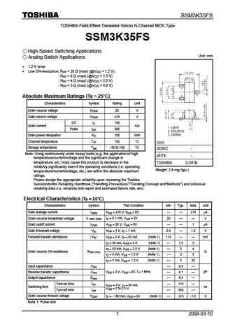
SSM3K35FS TOSHIBA Field-Effect Transistor Silicon N-Channel MOS Type SSM3K35FS High-Speed Switching Applications Unit mm Analog Switch Applications 1.2-V drive Low ON-resistance Ron = 20 (max) (@VGS = 1.2 V) Ron = 8 (max) (@VGS = 1.5 V) Ron = 4 (max) (@VGS = 2.5 V) Ron = 3 (max) (@VGS = 4.0 V) Absolute Maximum Ratings (Ta = 25 C)
ssm3k15afu.pdf
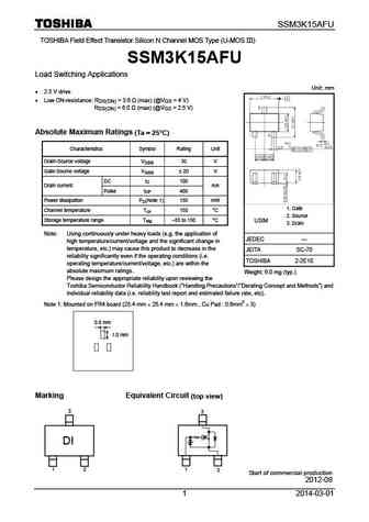
SSM3K15AFU TOSHIBA Field Effect Transistor Silicon N Channel MOS Type (U-MOS III) SSM3K15AFU Load Switching Applications Unit mm 2.5 V drive Low ON-resistance RDS(ON) = 3.6 (max) (@VGS = 4 V) RDS(ON) = 6.0 (max) (@VGS = 2.5 V) Absolute Maximum Ratings (Ta = 25 C) Characteristics Symbol Rating Unit Drain-Source voltage VDSS 30 V Gate-Source voltage VGSS 2
ssm3k48fu.pdf
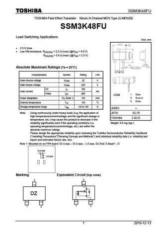
SSM3K48FU TOSHIBA Field Effect Transistor Silicon N Channel MOS Type (U-MOSIII) SSM3K48FU Load Switching Applications Unit mm 2.5-V drive Low ON-resistance RDS(ON) = 3.2 (max) (@VGS = 4.0 V) RDS(ON) = 5.4 (max) (@VGS = 2.5 V) Absolute Maximum Ratings (Ta = 25 C) Characteristics Symbol Rating Unit Drain-Source voltage VDSS 30 V Gate-Source voltage VGSS 20 V
ssm3k131tu.pdf
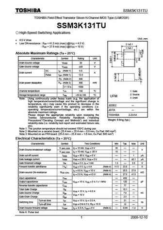
SSM3K131TU TOSHIBA Field-Effect Transistor Silicon N-Channel MOS Type (U-MOS ) SSM3K131TU High-Speed Switching Applications Unit mm 4.5-V drive Low ON-resistance Ron = 41.5 m (max) (@VGS = 4.5 V) 2.1 0.1 Ron = 27.6 m (max) (@VGS = 10 V) 1.7 0.1 Absolute Maximum Ratings (Ta = 25 C) 1 Characteristic Symbol Rating Unit 3 2 Drain-Source voltage VDSS
ssm3k03fv.pdf
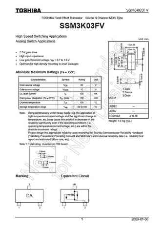
SSM3K03FV TOSHIBA Field Effect Transistor Silicon N Channel MOS Type SSM3K03FV High Speed Switching Applications Unit mm Analog Switch Applications 1.2 0.05 0.8 0.05 2.5-V gate drive High input impedance 1 Low gate threshold voltage Vth = 0.7 to 1.3 V Optimum for high-density mounting in small packages 3 2 Absolute Maximum Ratings (Ta = 25 C) Char
ssm3k35mfv.pdf
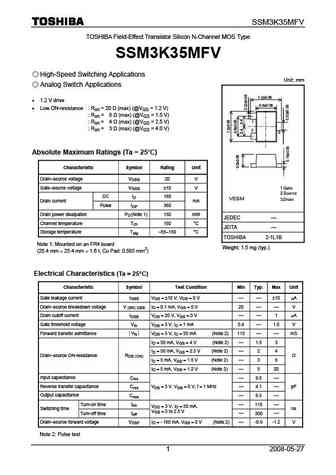
SSM3K35MFV TOSHIBA Field-Effect Transistor Silicon N-Channel MOS Type SSM3K35MFV High-Speed Switching Applications Unit mm Analog Switch Applications 1.2 0.05 1.2 V drive 0.8 0.05 Low ON-resistance Ron = 20 (max) (@VGS = 1.2 V) Ron = 8 (max) (@VGS = 1.5 V) 1 Ron = 4 (max) (@VGS = 2.5 V) Ron = 3 (max) (@VGS = 4.0 V) 2 3 Absolu
ssm3k345r.pdf
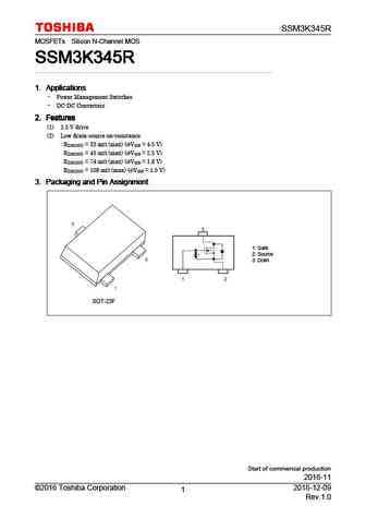
SSM3K345R MOSFETs Silicon N-Channel MOS SSM3K345R SSM3K345R SSM3K345R SSM3K345R 1. Applications 1. Applications 1. Applications 1. Applications Power Management Switches DC-DC Converters 2. Features 2. Features 2. Features 2. Features (1) 1.5 V drive (2) Low drain-source on-resistance RDS(ON) = 33 m (max) (@VGS = 4.5 V) RDS(ON) = 45 m (max) (@VGS = 2.5 V) R
ssm3k7002f.pdf
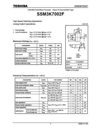
SSM3K7002F TOSHIBA Field-Effect Transistor Silicon N Channel MOS Type SSM3K7002F High-Speed Switching Applications Unit mm Analog Switch Applications +0.5 2.5-0.3 Small package +0.25 1.5-0.15 Low ON-resistance Ron = 3.3 (max) (@VGS = 4.5 V) Ron = 3.2 (max) (@VGS = 5 V) 1 Ron = 3.0 (max) (@VGS = 10 V) 2 3 Maximum Ratings (Ta = 25 C) Charact
ssm3k04fu.pdf
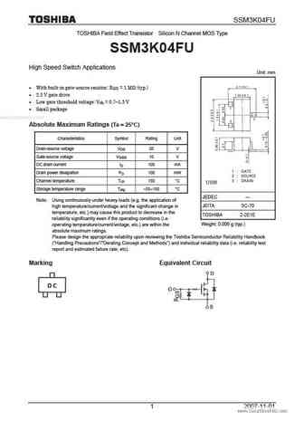
SSM3K04FU TOSHIBA Field Effect Transistor Silicon N Channel MOS Type SSM3K04FU High Speed Switch Applications Unit mm With built-in gate-source resistor RGS = 1 M (typ.) 2.5 V gate drive Low gate threshold voltage Vth = 0.7 1.3 V Small package www.DataSheet4U.com Absolute Maximum Ratings (Ta = 25 C) Characteristics Symbol Rating Unit Drain-source vol
ssm3k72kfs.pdf
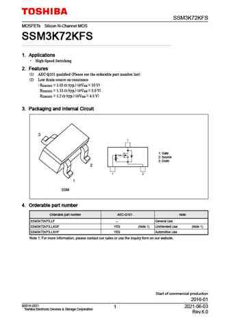
SSM3K72KFS MOSFETs Silicon N-Channel MOS SSM3K72KFS 1. Applications High-Speed Switching 2. Features (1) AEC-Q101 qualified (Please see the orderable part number list) (2) Low drain-source on-resistance RDS(ON) = 1.05 (typ.) (@VGS = 10 V) RDS(ON) = 1.15 (typ.) (@VGS = 5.0 V) RDS(ON) = 1.2 (typ.) (@VGS = 4.5 V) 3. Packaging and Internal Circuit 1 Gate 2 Source
ssm3k44fs.pdf
SSM3K44FS TOSHIBA Field Effect Transistor Silicon N Channel MOS Type SSM3K44FS High Speed Switching Applications Unit mm Analog Switching Applications Compact package suitable for high-density mounting Low ON-resistance RDS(ON) = 4.0 (max) (@VGS = 4 V) RDS(ON) = 7.0 (max) (@VGS = 2.5 V) Absolute Maximum Ratings (Ta = 25 C) Characteristic Symbol Rating U
ssm3k36tu.pdf
SSM3K36TU TOSHIBA Field-Effect Transistor Silicon N-Channel MOS Type SSM3K36TU High-Speed Switching Applications Unit mm 1.5-V drive Low ON-resistance Ron = 1.52 (max) (@VGS = 1.5 V) 2.1 0.1 Ron = 1.14 (max) (@VGS = 1.8 V) 1.7 0.1 Ron = 0.85 (max) (@VGS = 2.5 V) Ron = 0.66 (max) (@VGS = 4.5 V) 1 Ron = 0.63 (max) (@VGS = 5.0 V) 3
ssm3k35ct.pdf
SSM3K35CT TOSHIBA Field-Effect Transistor Silicon N-Channel MOS Type SSM3K35CT High-Speed Switching Applications Unit mm Analog Switch Applications 1.2-V drive Low ON-resistance Ron = 20 (max) (@VGS = 1.2 V) Ron = 8 (max) (@VGS = 1.5 V) Ron = 4 (max) (@VGS = 2.5 V) Ron = 3 (max) (@VGS = 4.0 V) Absolute Maximum Ratings (Ta = 25 C)
ssm3k106tu.pdf
SSM3K106TU TOSHIBA Field Effect Transistor Silicon N Channel MOS Type SSM3K106TU High-Speed Switching Applications Unit mm 2.1 0.1 4 V drive 1.7 0.1 Low ON-resistance Ron = 530 m (max) (@VGS = 4 V) Ron = 310 m (max) (@VGS = 10 V) Lead (Pb)-free 1 2 3 Maximum Ratings (Ta = 25 C) Characteristic Symbol Rating Unit Drain-source voltage VDS 20 V Gate-
ssm3k324r.pdf
SSM3K324R MOSFETs Silicon N-Channel MOS SSM3K324R SSM3K324R SSM3K324R SSM3K324R 1. Applications 1. Applications 1. Applications 1. Applications Power Management Switches DC-DC Converters 2. Features 2. Features 2. Features 2. Features (1) 1.8-V gate drive voltage. (2) Low drain-source on-resistance RDS(ON) = 56 m (max) (@VGS = 4.5 V) RDS(ON) = 72 m (max) (@VG
ssm3k333r.pdf
SSM3K333R TOSHIBA Field-Effect Transistor Silicon N-Channel MOS Type (U-MOS VII-H) SSM3K333R Power Management Switch Applications Unit mm High-Speed Switching Applications +0.08 0.42 +0.08 -0.05 0.17 0.05 M A -0.07 3 4.5V drive Low ON-resistance RDS(ON) = 42 m (max) (@VGS = 4.5 V) RDS(ON) = 28 m (max) (@VGS = 10 V) 1 2 0.95 0.95 Absolute Maxi
ssm3k16ct.pdf
SSM3K16CT TOSHIBA Field Effect Transistor Silicon N-Channel MOS Type SSM3K16CT High-Speed Switching Applications Unit mm Analog Switch Applications Suitable for high-density mounting due to compact package 0.6 0.05 0.5 0.03 Low ON-resistance Ron = 3.0 (max) (@VGS = 4 V) Ron = 4.0 (max) (@VGS = 2.5 V) Ron = 15 (max) (@VGS = 1.5 V) Absolute
ssm3k303t.pdf
SSM3K303T TOSHIBA Field Effect Transistor Silicon N Channel MOS Type SSM3K303T High Speed Switching Applications Unit mm 4 V drive Low ON-resistance Ron = 120 m (max) (@VGS = 4V) Ron = 83 m (max) (@VGS = 10V) Absolute Maximum Ratings (Ta = 25 C) Characteristic Symbol Rating Unit Drain source voltage VDS 30 V Gate source voltage VGSS 20 V DC ID 2.9
ssm3k316t.pdf
SSM3K316T TOSHIBA Field Effect Transistor Silicon N Channel MOS Type SSM3K316T Power Management Switch Applications High-Speed Switching Applications Unit mm 1.8-V drive Low ON-resistance Ron = 131 m (max) (@VGS = 1.8 V) Ron = 87 m (max) (@VGS = 2.5 V) Ron = 65 m (max) (@VGS = 4.5 V) Ron = 53 m (max) (@VGS = 10 V) Absolute Maximum Ratings (Ta = 25 C) Ch
ssm3k43fs.pdf
SSM3K43FS TOSHIBA Field-Effect Transistor Silicon N Channel MOS Type SSM3K43FS High-Speed Switching Applications Unit mm 1.5-V drive Low ON-resistance Ron = 1.52 (max) (@VGS = 1.5V) Ron = 1.14 (max) (@VGS = 1.8V) Ron = 0.85 (max) (@VGS = 2.5V) Ron = 0.66 (max) (@VGS = 4.5V) Ron = 0.63 (max) (@VGS = 5.0V) Absolute Maximum Ratings (
ssm3k15te.pdf
www.DataSheet4U.com SSM3K15TE TOSHIBA Field Effect Transistor Silicon N Channel MOS Type SSM3K15TE High Speed Switching Applications Unit mm Analog Switch Applications 1.2 0.05 0.8 0.05 Small package Low on resistance Ron = 4.0 (max) (@VGS = 4 V) Ron = 7.0 (max) (@VGS = 2.5 V) Absolute Maximum Ratings (Ta = 25 C) Characteristics Symb
ssm3k333r.pdf
UNISONIC TECHNOLOGIES CO., LTD SSM3K333R Preliminary Power MOSFET 6A, 30V N-CHANNEL POWER MOSFET DESCRIPTION The UTC SSM3K333R is an N-channel power MOSFET using UTC s advanced technology to provide customers with a minimum on-state resistance and superior switching performance. The UTC SSM3K333R is usually used in power management switching applications. FEATURES * R
ssm3k301t.pdf
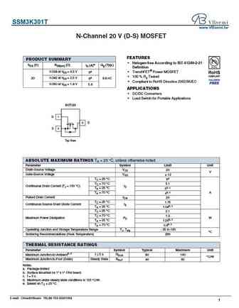
SSM3K301T www.VBsemi.tw N-Channel 20 V (D-S) MOSFET FEATURES PRODUCT SUMMARY Halogen-free According to IEC 61249-2-21 VDS (V) RDS(on) ( ) ID (A)e Qg (Typ.) Definition 0.028 at VGS = 4.5 V TrenchFET Power MOSFET 6a 100 % Rg Tested 20 0.042 at VGS = 2.5 V 6a 8.8 nC Compliant to RoHS Directive 2002/95/EC 0.050 at VGS = 1.8 V 5.6 APPLICATIONS DC/DC
ssm3k7002f.pdf
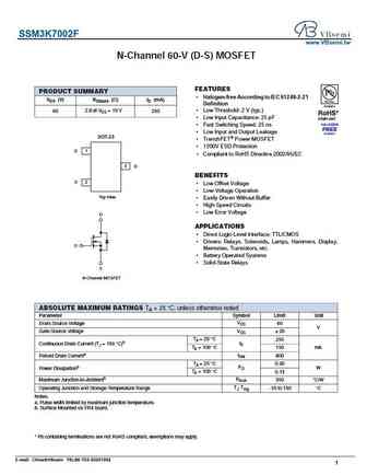
SSM3K7002F www.VBsemi.tw N-Channel 60-V (D-S) MOSFET FEATURES PRODUCT SUMMARY Halogen-free According to IEC 61249-2-21 VDS (V) RDS(on) ( )ID (mA) Definition 2.8 at VGS = 10 V 60 250 Low Threshold 2 V (typ.) Low Input Capacitance 25 pF Fast Switching Speed 25 ns Low Input and Output Leakage SOT-23 TrenchFET Power MOSFET 1200V ESD Protection G
ssm3k335.pdf

SSM3K335 www.VBsemi.tw N-Channel 30-V (D-S) MOSFET FEATURES PRODUCT SUMMARY Halogen-free According to IEC 61249-2-21 VDS (V) RDS(on) ( ) ID (A)a Qg (Typ.) Definition 0.030 at VGS = 10 V TrenchFET Power MOSFET 6.5 30 4.5 nC 100 % Rg Tested 0.033 at VGS = 4.5 V 6.0 Compliant to RoHS Directive 2002/95/EC APPLICATIONS DC/DC Converter D TO-236 (SOT-23) G
ssm3k333r.pdf
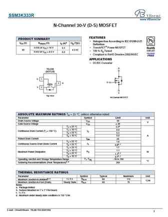
SSM3K333R www.VBsemi.tw N-Channel 30-V (D-S) MOSFET FEATURES PRODUCT SUMMARY Halogen-free According to IEC 61249-2-21 VDS (V) RDS(on) ( ) ID (A)a Qg (Typ.) Definition 0.030 at VGS = 10 V TrenchFET Power MOSFET 6.5 30 4.5 nC 100 % Rg Tested 0.033 at VGS = 4.5 V 6.0 Compliant to RoHS Directive 2002/95/EC APPLICATIONS DC/DC Converter D TO-236 (SOT-23)
Другие IGBT... SSM2603GY, SSM2603Y, SSM2605GY, SSM2761P-A, SSM3310GH, SSM3310GJ, SSM3J331R, SSM3J338R, IRFZ46N, SSM3K318R, SSM3K324R, SSM3K335R, SSM3K336R, SSM3K337R, SSM3K339R, SSM3K35CTC, SSM3K56CT
History: SSM3310GJ
🌐 : EN ES РУ

Список транзисторов
Обновления
MOSFET: BCD70N07A | BCD90N03 | BCD80N06 | T50N06 | H50N06 | BCD12N65 | BCT12N65 | BCD4N65 | BCT4N65 | BCD7N65 | BCT7N65 | BCT20N65 | ASDM30P100KQ | ASDM30N90Q | ASDM30N75KQ | ASDM30N150Q
Popular searches
c2075 transistor | ecg123 | 2n5551 transistor equivalent | 13009 datasheet | 3dd15d transistor | pa110bda | 2sb1243 | a1123 transistor